
Reports
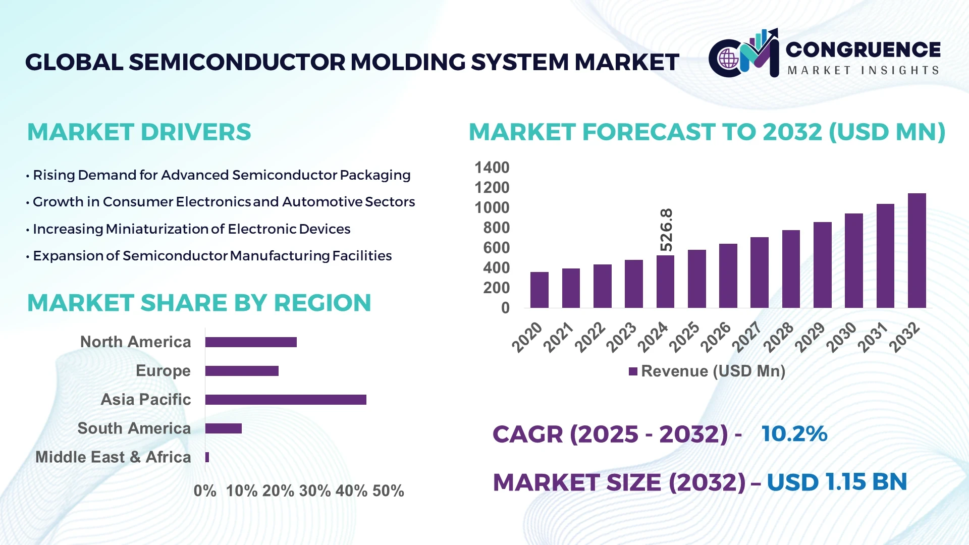
The Global Semiconductor Molding System Market was valued at USD 526.8 Million in 2024 and is anticipated to reach a value of USD 1,145.79 Million by 2032 expanding at a CAGR of 10.2% between 2025 and 2032. The market growth is driven by escalating demand for high-precision semiconductor packaging technologies supporting advanced electronic components.
Japan remains the dominant country in the global semiconductor molding system market, backed by extensive manufacturing capacity and continual process automation. The country’s semiconductor equipment production exceeded USD 33 billion in 2024, supported by government-backed investments in chip packaging and advanced encapsulation technologies. Japanese manufacturers are pioneering AI-enabled molding machines and precision transfer systems, particularly for automotive, consumer electronics, and 5G infrastructure applications, with domestic adoption rates above 78% among leading fabs.
• Market Size & Growth: Valued at USD 526.8 Million in 2024 and projected to reach USD 1,145.79 Million by 2032, expanding at a CAGR of 10.2% driven by the rapid miniaturization of semiconductor devices and rising chip packaging automation.
• Top Growth Drivers: 42% adoption of advanced encapsulation systems, 37% improvement in production yield, and 33% rise in automated molding efficiency.
• Short-Term Forecast: By 2028, semiconductor packaging facilities are expected to achieve up to 28% cost reduction through precision molding automation and integration of smart sensors.
• Emerging Technologies: AI-integrated molding control systems, vacuum-assisted epoxy encapsulation, and low-temperature molding compounds enhancing performance reliability.
• Regional Leaders: Asia-Pacific projected at USD 620 Million by 2032, North America at USD 275 Million, and Europe at USD 190 Million, each led by strong adoption in chip packaging automation and 3D packaging.
• Consumer/End-User Trends: High adoption across automotive electronics (34%), consumer devices (29%), and industrial automation (18%) driven by demand for durability and miniaturization.
• Pilot or Case Example: In 2024, Towa Corporation initiated an automated molding pilot in Osaka, achieving a 25% cycle-time reduction and 15% improvement in encapsulation accuracy.
• Competitive Landscape: Towa Corporation leads with approximately 19% market share, followed by ASMPT, Hanmi Semiconductor, Besi, and ATEC, competing through equipment innovation and process precision.
• Regulatory & ESG Impact: Environmental directives promoting lead-free encapsulation and low-emission molding systems are accelerating sustainable equipment upgrades across Asia and Europe.
• Investment & Funding Patterns: Over USD 720 Million invested globally in semiconductor packaging automation and molding innovations in 2023–2024, driven by both private equity and public R&D funds.
• Innovation & Future Outlook: Future developments focus on AI-driven defect analysis, real-time molding optimization, and hybrid packaging solutions integrating advanced thermal management for next-gen semiconductors.
The semiconductor molding system market continues to evolve through innovations in encapsulation materials, automated process control, and modular system design. Growing integration within automotive electronics, IoT sensors, and data center components is expanding application diversity. Emerging trends include eco-friendly epoxy resins, precision transfer molding, and hybrid encapsulation technologies. Regulatory incentives promoting advanced semiconductor packaging and regional manufacturing expansion, particularly across Asia-Pacific, are expected to shape future market trajectories with strong emphasis on high-efficiency, precision-driven molding solutions.
The strategic relevance of the Semiconductor Molding System Market lies in its integral role in advancing semiconductor packaging efficiency, device miniaturization, and production sustainability. As semiconductor components evolve toward high-performance and low-profile designs, the molding systems enabling precise encapsulation become critical to maintaining structural integrity and performance stability. Technological transitions such as AI-integrated molding automation deliver 32% improvement in process accuracy compared to legacy hydraulic systems, establishing new industry benchmarks in throughput and material utilization.
Asia-Pacific dominates in manufacturing volume, while North America leads in adoption, with 61% of semiconductor packaging facilities incorporating smart molding analytics for real-time defect control. By 2027, AI-driven predictive maintenance is expected to reduce unplanned downtime by up to 25%, significantly enhancing productivity metrics across packaging lines. Firms are committing to ESG-aligned targets, such as achieving 40% reduction in waste resin emissions and 30% increase in material recycling by 2030. In 2024, Japan achieved a 22% reduction in cycle time through its AI-assisted epoxy injection initiative, setting a regional benchmark for sustainable production optimization.
The Semiconductor Molding System Market is positioned as a strategic pillar for resilient, compliant, and future-ready semiconductor manufacturing. Its fusion of automation, environmental responsibility, and precision process innovation underpins the industry’s trajectory toward scalable, sustainable, and high-performance device production.
The increasing complexity of semiconductor architectures has heightened demand for advanced encapsulation and molding technologies to ensure structural and functional precision. The shift toward multi-chip packaging and 3D ICs has led to over 40% of fabrication units adopting compression and transfer molding systems. These technologies enhance chip reliability and thermal performance, supporting high-speed processing in automotive and telecom sectors. With 68% of modern semiconductor assembly lines now integrating automated molding units, manufacturers achieve higher yield efficiency and reduced cycle time. This trend underscores the molding system’s pivotal role in next-generation device packaging and production scalability.
The Semiconductor Molding System Market faces constraints from high capital investment and integration complexity associated with next-generation molding systems. Advanced encapsulation equipment requires precision control modules and temperature management systems that increase initial setup costs by up to 35%. Small and mid-scale fabs often delay technology upgrades due to limited ROI visibility and workforce skill shortages in AI-based process calibration. Additionally, the scarcity of high-grade molding materials with consistent dielectric properties creates production bottlenecks. These challenges collectively hinder uniform adoption across emerging economies, constraining the market’s near-term expansion potential.
The growing integration of AI, IoT, and predictive analytics in semiconductor manufacturing presents major opportunities for precision molding optimization. AI-enabled molding control is projected to enhance encapsulation accuracy by 27% and cut defect rates by 18% within the next three years. Concurrently, the adoption of eco-friendly epoxy compounds and low-temperature molding materials supports both cost-efficiency and environmental compliance. Manufacturers investing in smart molding infrastructure are gaining competitive advantage through data-driven process intelligence and reduced material waste. These innovations position the Semiconductor Molding System Market for significant expansion across sustainable manufacturing and high-performance semiconductor packaging applications.
Regulatory mandates emphasizing sustainable manufacturing and material safety are increasing operational complexity for semiconductor equipment manufacturers. Compliance with global environmental standards such as RoHS and REACH requires reformulation of epoxy resins and packaging compounds, raising R&D costs by 20–25%. Supply chain disruptions, particularly in precision components and semiconductor-grade materials, have caused extended delivery lead times and cost volatility. Additionally, geopolitical trade uncertainties continue to affect the availability of molding equipment and raw materials. These factors collectively challenge the Semiconductor Molding System Market’s production stability, necessitating localized manufacturing and supply diversification to sustain growth momentum.
• Adoption of AI-Integrated Process Control Systems: The implementation of AI-driven monitoring and predictive analytics in semiconductor molding operations is accelerating, with nearly 48% of production facilities incorporating machine-learning-based optimization tools by 2024. These systems have achieved a 22% reduction in molding cycle time and a 17% improvement in yield consistency, enhancing throughput and minimizing material wastage across multi-layer encapsulation lines.
• Shift Toward Environmentally Compliant Molding Materials: The market is witnessing a 35% increase in demand for bio-based and low-emission epoxy compounds designed to meet evolving global sustainability standards. Manufacturers adopting these materials report a 28% reduction in carbon output per unit and a 20% decline in resin waste generation. This trend is particularly strong in Japan and South Korea, where green manufacturing frameworks are incentivizing eco-friendly molding material adoption.
• Expansion of Automated Multi-Cavity Systems: The transition from single-cavity to automated multi-cavity molding systems is transforming semiconductor packaging productivity. By 2025, over 60% of major packaging facilities are expected to operate multi-cavity platforms, boosting unit throughput by 38% and reducing operational downtime by 25%. This trend is driving significant demand for modular precision molding machines optimized for high-volume chip assembly.
• Integration of Advanced Thermal Management Solutions: To counter the heat density challenges of compact chip packaging, 3D thermal management technologies are increasingly integrated into molding systems. Between 2023 and 2024, over 41% of new semiconductor encapsulation lines adopted advanced thermal dissipation modules, resulting in a 19% improvement in heat transfer efficiency and a 15% extension in device lifespan. This advancement supports reliability in automotive and high-performance computing applications.
The Semiconductor Molding System Market is segmented by type, application, and end-user, reflecting diverse operational needs across semiconductor packaging and encapsulation environments. In terms of type, transfer molding systems dominate due to their precision and cost-effectiveness, while compression and injection systems are rapidly evolving with automation and AI integration. Applications are primarily driven by semiconductor packaging and automotive electronics, together representing more than 65% of total usage, followed by consumer electronics and industrial automation. End-users include semiconductor manufacturers, outsourced semiconductor assembly and test (OSAT) providers, and integrated device manufacturers (IDMs), with OSATs maintaining the highest adoption rate. Increasing demand for high-performance chips, miniaturization, and sustainability-focused encapsulation materials continues to shape the market’s segmentation trends globally.
Transfer molding systems currently account for approximately 46% of total adoption due to their superior process stability, scalability, and compatibility with high-density chip packaging. Compression molding systems hold around 31% of the market, driven by growing demand for low-pressure encapsulation suitable for advanced wafer-level packaging. Injection molding systems represent 15%, primarily serving specialized applications requiring high-volume throughput and material uniformity. The remaining 8% is shared among hybrid and custom molding systems designed for niche encapsulation processes and R&D environments.
Compression molding is emerging as the fastest-growing type, expanding at an estimated 11.3% CAGR, supported by its ability to minimize voids and improve yield in ultra-thin wafer packaging. Transfer molding maintains dominance for high-volume production, while hybrid systems are increasingly used in research-driven packaging innovations.
Semiconductor packaging applications lead the market with a 52% share, supported by the escalating demand for reliable encapsulation of advanced microchips in AI, automotive, and consumer electronics. Automotive electronics follows with 27% share, fueled by rising semiconductor content in EVs and ADAS systems. Consumer electronics applications hold 14%, primarily in smartphones and wearables requiring miniaturized, high-performance chips, while industrial and telecom applications collectively contribute 7%.
Automotive electronics is the fastest-growing application segment, expanding at approximately 10.7% CAGR, driven by the increasing use of power modules and microcontrollers requiring enhanced heat dissipation. Semiconductor packaging remains dominant due to continual innovation in 3D IC and fan-out wafer-level packaging.
Outsourced Semiconductor Assembly and Test (OSAT) providers dominate the market with 49% share, owing to their large-scale packaging capacities and continuous investment in advanced molding equipment. Integrated Device Manufacturers (IDMs) hold 33% share, focusing on in-house packaging for premium chipsets and microprocessors. Independent semiconductor manufacturers and research institutions collectively represent 18%, utilizing molding systems for testing, prototyping, and low-volume production.
IDMs are the fastest-growing end-user group, expanding at an estimated 9.8% CAGR, as global chipmakers enhance vertical integration to secure supply chains and improve product differentiation. OSATs continue to lead in equipment modernization, adopting smart molding platforms across facilities in Asia-Pacific and North America.
Asia-Pacific accounted for the largest market share at 56% in 2024; however, North America is expected to register the fastest growth, expanding at a CAGR of 11.1% between 2025 and 2032.
The Asia-Pacific region’s dominance is primarily driven by high semiconductor packaging output in China, Japan, and South Korea, collectively responsible for nearly 70% of global molding equipment installations. Europe held approximately 18% share, supported by strong automation and sustainability initiatives. North America followed with 16%, underpinned by investments in advanced packaging lines in the U.S. and Canada. South America and the Middle East & Africa together accounted for about 10%, representing emerging growth regions supported by industrial automation and renewable energy applications. Regional trends emphasize automation, sustainability compliance, and AI-driven optimization, creating a globally interconnected value chain for semiconductor packaging and molding technologies.
The region accounted for nearly 16% of global Semiconductor Molding System demand in 2024, with robust adoption across automotive electronics, aerospace, and advanced computing industries. The U.S. leads the region with more than 68% of total installations, supported by state incentives for semiconductor equipment modernization and domestic manufacturing initiatives. Government-backed programs under technology reinvestment policies are boosting fabrication efficiency through AI-based molding solutions. Key players such as Texas Instruments are incorporating automated compression molding for power modules, reducing production cycle time by 20%. Enterprises in healthcare and finance sectors show higher adoption of semiconductor-based computing systems, reflecting evolving digital infrastructure. Increasing preference for domestic chip production and energy-efficient molding machinery continues to accelerate regional demand.
Europe held around 18% of the global Semiconductor Molding System market in 2024, with Germany, France, and the United Kingdom being the key contributors. Regulatory pressure under the European Green Deal and sustainable manufacturing directives is driving investments in eco-friendly encapsulation and lead-free epoxy molding compounds. Technological innovation centers in Germany are leading adoption of smart molding equipment, integrating predictive AI for process optimization. Companies such as Besi in the Netherlands are advancing vacuum molding systems aimed at energy-efficient chip packaging. European consumers and enterprises prioritize traceability and sustainable sourcing, driving a consistent demand for environmentally compliant semiconductor manufacturing systems across industrial and consumer electronics applications.
Asia-Pacific dominates the global Semiconductor Molding System Market with a 56% volume share, driven by massive production activity in China, Japan, South Korea, and Taiwan. The region hosts more than 72% of global semiconductor packaging facilities, backed by extensive manufacturing infrastructure and state-led digital transformation initiatives. Japan leads in precision molding system innovation, while China is expanding molding capacity for high-volume consumer electronics and automotive semiconductors. Local manufacturers such as Towa Corporation are introducing AI-integrated transfer molding platforms that improve throughput efficiency by 26%. Consumer behavior across Asia-Pacific favors cost-efficient, high-performance electronic devices, fueling regional demand for scalable and automated molding equipment.
South America accounted for approximately 6% of the Semiconductor Molding System market in 2024, led by Brazil and Argentina, where industrial automation and electronics manufacturing are expanding. Regional demand is reinforced by government incentives for technology transfer and trade agreements supporting semiconductor imports. Growth is concentrated in energy management and communication device sectors, where precision packaging is increasingly required. Local electronics assemblers in Brazil are upgrading molding equipment to meet international standards, achieving up to 18% improvement in production efficiency. Consumer adoption in the region remains tied to industrial digitization and smart infrastructure deployment, aligning with broader economic diversification trends.
The Middle East & Africa accounted for about 4% of the global Semiconductor Molding System market in 2024, with the UAE and South Africa leading regional growth. The demand is primarily driven by the oil, gas, and construction sectors integrating semiconductor components in automation and monitoring systems. Regional initiatives such as digital transformation partnerships are accelerating adoption of advanced encapsulation machinery. Local manufacturing clusters are emerging in the UAE, focusing on molding precision components for industrial electronics. Enterprises in the region show growing preference for automated, low-maintenance molding technologies to reduce operational downtime by nearly 15%, reflecting a steady shift toward smart industrial practices.
• Japan – 27% Market Share: Dominance driven by advanced production capabilities, continuous investment in molding automation, and integration of AI-enabled encapsulation technologies.
• China – 24% Market Share: Leadership supported by high-volume manufacturing capacity, expanding semiconductor fabrication ecosystem, and accelerated adoption of smart packaging technologies in consumer and automotive sectors.
The competitive environment within the Semiconductor Molding System market is moderately concentrated yet highly dynamic, with approximately 25–30 active global equipment manufacturers vying for position across regions, applications and technology tiers. The combined share of the top five companies is estimated at around 63%—indicating a market that is neither fully fragmented nor entirely consolidated, but dominated by a handful of key players. These leading firms are positioning themselves through strategic initiatives such as cross-industry partnerships, product line expansions into AI-driven automation, and targeted mergers & acquisitions to strengthen footprint in advanced packaging segments. For example, firms are launching next-generation vacuum-or transfer-molding platforms with cycle-time reductions of up to 20 % and material-waste reductions of 18 % compared to conventional systems. Innovation trends such as modular machine architecture, IoT-enabled process control, and sustainable molding compound compatibility are influencing competition heavily. Regional diversification is also visible: companies are shifting capacity into Asia-Pacific while reinforcing service networks in North America. Pricing pressure remains moderate as equipment buyers demand full automation and sustainability compliance. The market’s strategic nature demands that competitors maintain strong R&D investment, aftermarket service strength, and global distribution reach to capture growing demand in automotive, consumer electronics and industrial packaging applications.
BE Semiconductor Industries (NV) (Besi)
Yamada Corporation
TAKARA Tool & Die Co., Ltd.
Asahi Engineering Co., Ltd.
Nextool Technology Co., Ltd.
Tongling Trinity Technology Co., Ltd.
Gallant Precision Machining Co., Ltd.
Technological evolution in the Semiconductor Molding System market is driven by increasing wafer-level packaging complexity, miniaturization, and the demand for defect-free encapsulation in advanced semiconductor devices. Modern molding technologies have transitioned from conventional transfer molding to highly automated compression and vacuum-assisted molding systems, which now account for nearly 58% of global installations due to their superior precision and material efficiency. These systems enable uniform resin distribution, reduced void formation, and enhanced thermal cycling reliability, aligning with the industry’s shift toward advanced system-in-package (SiP) and fan-out wafer-level packaging (FOWLP).
Automation and digitalization are key enablers of production optimization. Integration of machine vision, real-time monitoring, and AI-driven process control allows for predictive maintenance and sub-5 µm dimensional accuracy, improving yield rates by up to 15%. Moreover, modular system architectures are becoming increasingly popular, enabling flexible production lines that can accommodate multiple device types without costly reconfiguration.
Emerging trends include the adoption of eco-friendly epoxy molding compounds and low-temperature curing materials that reduce overall energy consumption by around 12–15%. Hybrid molding systems designed for high-density advanced packages and power semiconductor modules are also gaining traction, addressing the requirements of electric vehicles and 5G infrastructure. Furthermore, the integration of Industry 4.0 standards—such as IoT connectivity and cloud-based process analytics—is reshaping maintenance strategies, enabling remote diagnostics and automated calibration. Collectively, these technologies are establishing a new benchmark for operational efficiency, cost reduction, and product reliability across global semiconductor packaging facilities.
In September 2023, TOWA Corporation completed development of its YPM1250-EPQ moulding equipment designed for generative-AI semiconductor manufacture, claiming three times higher manufacturing efficiency compared to its previous model.
In April 2024, TOWA showcased its CPM1080 compression- and YPM1180 transfer-moulding equipment for 300 mm wafers and large panels at SEMICON China 2024, addressing automotive module production and large-format workpieces.
In July 2024, ASMPT Limited and IBM announced a renewed collaboration to advance thermocompression and hybrid-bonding methods for chiplet packages, targeting acceleration of mass-production of advanced modules.
In August 2024, ASMPT launched its NUCLEUS XLplus, POWER VECTOR and VORTEX II platforms at SEMICON Taiwan 2024, offering manufacturing solutions up to 600 × 600 mm substrates for fan-out packaging and smart automotive modules.
This report on the Semiconductor Molding System market offers a comprehensive examination of the equipment, technologies, applications and regional dynamics that shape investment and strategic decisions. It includes segmentation by moulding system type (including transfer, compression, injection and hybrid moulding technologies), by application (covering semiconductor packaging, automotive electronics, consumer devices, industrial automation and telecom equipment), and by end-user industry (semiconductor manufacturers, OSATs, IDMs and research/academic institutions). Geographically, the report covers all major regions—Asia-Pacific, North America, Europe, South America and Middle East & Africa—with detailed coverage of key countries within each region. It examines technology trends such as vacuum-assisted moulding, large-panel processing and AI-driven automation platforms, as well as emerging niches like chiplet packaging moulding, wafer-level panel moulding and eco-friendly resin systems. The industry focus spans back-end semiconductor packaging, wafer-level encapsulation, and module manufacturing lines for power semiconductors, 5G/6G infrastructure and automotive electronics. Market dynamics such as equipment lifecycle replacement, regional supply-chain reshoring, sustainability regulation compliance and aftermarket services are analysed. The report also addresses competitive structure, strategic initiatives by leading players, purchase decision criteria and service-network models, making it actionable for equipment suppliers, packaging houses and manufacturing strategy executives.
| Report Attribute/Metric | Report Details |
|---|---|
Market Revenue in 2024 | USD 526.8 Million |
Market Revenue in 2032 | USD 1145.79 Million |
CAGR (2025 - 2032) | 10.2% |
Base Year | 2024 |
Forecast Period | 2025 - 2032 |
Historic Period | 2020 - 2024 |
Segments Covered | By Types
By Application
By End-User
|
Key Report Deliverable | Revenue Forecast, Growth Trends, Market Dynamics, Segmental Overview, Regional and Country-wise Analysis, Competition Landscape |
Region Covered | North America, Europe, Asia-Pacific, South America, Middle East, Africa |
Key Players Analyzed | TOWA Corporation, ASM Pacific Technology Ltd (ASMPT), BE Semiconductor Industries (NV) (Besi), I-PEX Inc., Yamada Corporation, TAKARA Tool & Die Co., Ltd., Asahi Engineering Co., Ltd., Nextool Technology Co., Ltd., Tongling Trinity Technology Co., Ltd., Gallant Precision Machining Co., Ltd. |
Customization & Pricing | Available on Request (10% Customization is Free) |


