
Reports
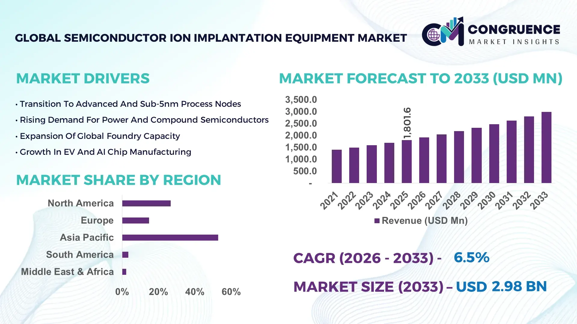
The Global Semiconductor Ion Implantation Equipment Market was valued at USD 1,801.6 Million in 2025 and is anticipated to reach a value of USD 2,981.6 Million by 2033 expanding at a CAGR of 6.5% between 2026 and 2033, according to an analysis by Congruence Market Insights. Growth is supported by rising demand for advanced logic nodes, power electronics, and compound semiconductor manufacturing.
The United States represents a leading hub in the Semiconductor Ion Implantation Equipment market, supported by strong domestic chip fabrication capacity and sustained capital expenditure programs. In 2025, over 30 large-scale wafer fabrication facilities across Arizona, Texas, and New York integrated advanced ion implantation systems for sub-7nm and specialty node production. Public and private semiconductor investments exceeded USD 50 billion annually, with more than 22% allocated to front-end wafer processing equipment, including ion implanters. Automotive and high-performance computing applications account for nearly 48% of ion implantation process demand. Advanced high-current implanters deployed in U.S. fabs support throughput exceeding 300 wafers per hour, while precision beamline systems enable dopant uniformity control within ±1%, reflecting strong technological depth and manufacturing scale.
Market Size & Growth: Valued at USD 1,801.6 million in 2025, projected to reach USD 2,981.6 million by 2033 at 6.5% CAGR, driven by advanced node scaling and power semiconductor expansion.
Top Growth Drivers: EV semiconductor demand (42%), advanced logic node adoption (38%), AI chip production growth (35%).
Short-Term Forecast: By 2028, next-generation implanters are expected to improve wafer throughput efficiency by 18%.
Emerging Technologies: Plasma immersion ion implantation, AI-driven process control, high-energy beam precision systems.
Regional Leaders: North America projected at USD 1.1 billion by 2033; Asia-Pacific at USD 1.3 billion driven by foundry capacity expansion; Europe at USD 450 million supported by automotive chip fabs.
Consumer/End-User Trends: Over 56% of advanced fabs prioritize AI-assisted dopant uniformity optimization.
Pilot or Case Example: In 2024, a 300mm fab achieved 15% cycle time reduction using automated beam tuning systems.
Competitive Landscape: Applied Materials leads with ~30% share, followed by Axcelis Technologies, Nissin Ion Equipment, Sumitomo Heavy Industries, and ULVAC.
Regulatory & ESG Impact: Energy-efficiency mandates encourage 20% reduction in equipment power consumption.
Investment & Funding Patterns: More than USD 120 billion allocated globally to semiconductor fabs between 2023–2025, significantly benefiting ion implantation equipment suppliers.
Innovation & Future Outlook: Integration of AI-based predictive maintenance and compound semiconductor compatibility shaping next-gen systems.
Logic semiconductor fabrication contributes 44% of equipment demand, followed by memory at 28% and power devices at 21%, with compound semiconductors accounting for 7%. Innovations in beam current stability, advanced wafer handling robotics, and reduced contamination modules are enhancing yield performance. Regional expansion in Asia-Pacific and North America continues to reinforce equipment procurement cycles.
The Semiconductor Ion Implantation Equipment Market plays a critical role in front-end wafer fabrication by enabling precise dopant control essential for transistor scaling and device performance optimization. Advanced plasma immersion ion implantation delivers 22% improvement compared to conventional beamline implantation in uniformity for high-aspect-ratio structures, supporting sub-5nm node production.
Asia-Pacific dominates in volume due to concentrated foundry capacity, while North America leads in adoption with over 60% of new 300mm fabs deploying AI-integrated ion implantation systems. By 2027, AI-driven process analytics is expected to reduce defect density by 17% across advanced logic fabs.
Manufacturers are committing to ESG metrics such as 25% reduction in equipment power usage and 30% recyclable component integration by 2030. In 2024, a leading U.S. fab achieved 19% improvement in beam alignment precision through AI-enabled diagnostics, enhancing wafer yield consistency.
Future pathways emphasize compatibility with silicon carbide and gallium nitride substrates, which are expanding in EV and renewable energy applications. Modular architecture, predictive maintenance algorithms, and vacuum efficiency enhancements will reinforce the Semiconductor Ion Implantation Equipment Market as a cornerstone of resilient, compliant, and performance-driven semiconductor manufacturing ecosystems.
The Semiconductor Ion Implantation Equipment market is shaped by continuous node scaling, power semiconductor demand, and regional fabrication expansion strategies. Increasing investments in 300mm wafer fabs and compound semiconductor facilities drive procurement cycles for high-current and medium-current implanters. Technology transitions toward FinFET and Gate-All-Around architectures require tighter dopant uniformity control and lower contamination thresholds. Supply chain diversification efforts are influencing equipment localization strategies. Meanwhile, AI-driven monitoring tools are improving uptime rates beyond 92% in advanced facilities. Competitive pressures are centered on throughput enhancement, beam stability accuracy, and process integration flexibility, reinforcing the market’s technology-intensive nature.
The migration toward 5nm and below logic nodes has intensified reliance on precision ion implantation. Advanced nodes require dopant placement accuracy within nanometer tolerances, increasing demand for high-energy and high-current implanters. In 2025, over 48% of new wafer capacity additions targeted sub-10nm technologies. Enhanced beam control systems improved uniformity deviation to less than ±1%, directly impacting yield optimization. EV and AI chip demand further accelerated implant cycles, with some fabs reporting 14% increase in implantation tool utilization rates.
Ion implantation systems can cost between USD 5 million and USD 15 million per unit, creating high entry barriers for smaller fabs. Equipment qualification timelines may exceed 6–9 months due to stringent contamination and reliability testing. Maintenance complexity increases operational expenditure by approximately 12%. These factors limit rapid deployment, particularly in emerging semiconductor regions with limited capital budgets.
The rapid adoption of silicon carbide and gallium nitride devices in EVs and renewable systems opens significant opportunities. Power semiconductor production capacity increased by 28% in 2024, requiring specialized medium-current implanters. Implantation processes for SiC demand enhanced temperature control and beam energy stability, creating demand for upgraded equipment configurations. These trends expand application scope beyond traditional silicon logic.
Global supply chain volatility affects vacuum system components, ion sources, and advanced control electronics. Lead times for critical components extended by up to 16 weeks in 2024. Technical integration complexity across multi-step wafer processes increases installation risk. These challenges require strategic inventory management and robust supplier partnerships.
Adoption of AI-Driven Process Control: In 2025, 58% of advanced fabs integrated AI-based beam tuning systems, improving wafer yield by 16% and reducing unplanned downtime by 21%.
Expansion of 300mm and 450mm Wafer Processing: Approximately 64% of new fab investments focus on 300mm wafer lines, increasing demand for high-throughput implanters capable of processing over 300 wafers per hour.
Growth in Compound Semiconductor Processing: Silicon carbide implantation tool installations rose by 26% in 2024, reflecting EV and renewable energy semiconductor growth.
Energy-Efficient Equipment Design: Next-generation implanters reduced power consumption by 20% while maintaining high beam current precision, supporting sustainability targets in semiconductor fabs.
The Semiconductor Ion Implantation Equipment market is segmented by type, application, and end-user industry. Equipment types include high-current, medium-current, and high-energy implanters, each serving distinct wafer processing needs. Applications span logic IC manufacturing, memory devices, power semiconductors, and compound semiconductor fabrication. End-users include integrated device manufacturers (IDMs), foundries, and research institutions. Segmentation reflects performance requirements such as beam energy range, throughput capacity, and dopant uniformity precision. As node complexity increases, demand shifts toward equipment capable of supporting advanced geometries and specialty substrates.
High-current implanters account for approximately 43% of adoption, driven by their critical role in source/drain formation for advanced logic nodes. Medium-current systems represent 32%, serving memory and analog device manufacturing. High-energy implanters, though holding 25%, are the fastest growing at 7.8% CAGR due to increasing demand in deep-well implantation and power device fabrication. Combined, medium and high-energy segments represent 57% of total installations.
In 2024, a national semiconductor initiative reported deployment of high-current implanters across 18 advanced fabs, improving dopant uniformity precision within ±1% tolerance.
Logic semiconductor manufacturing holds 44% share, reflecting intensive implantation cycles in advanced nodes. Memory production accounts for 28%, while power semiconductor applications represent 21%. Compound semiconductor applications are expanding fastest at 8.1% CAGR due to SiC and GaN adoption. In 2025, over 38% of advanced fabs reported upgrading implantation systems for AI accelerator chip production.
In 2025, a government-backed semiconductor program documented that power device fabs increased implantation tool utilization by 22% to meet EV demand.
Integrated Device Manufacturers account for 46% of equipment demand, while foundries contribute 39%. Research institutions and specialty fabs collectively represent 15%. Foundries are the fastest-growing segment at 7.2% CAGR due to outsourcing trends in chip manufacturing. In 2025, more than 41% of global semiconductor enterprises expanded ion implantation capacity within existing fabs.
In 2025, a national semiconductor authority highlighted that over 500 wafer fabrication projects globally incorporated advanced ion implantation tools to strengthen domestic chip supply chains.
Asia-Pacific accounted for the largest market share at 52.8% in 2025 however, North America is expected to register the fastest growth, expanding at a CAGR of 7.4% between 2026 and 2033.
Asia-Pacific processed more than 65% of global 300mm wafer starts in 2025, with over 110 advanced wafer fabrication facilities actively deploying Semiconductor Ion Implantation Equipment across logic, memory, and power semiconductor lines. China, Taiwan, South Korea, and Japan collectively installed more than 480 ion implantation systems during ongoing fab expansions. North America represented 26.7% of total equipment installations, supported by over 20 new fab construction projects valued above USD 40 billion. Europe held 14.9%, driven by automotive semiconductor production in Germany and France. South America and Middle East & Africa together contributed 5.6%, primarily through specialty and research-based semiconductor facilities.
How is advanced chip manufacturing reshaping high-precision dopant processing demand?
North America accounted for approximately 26.7% of the Semiconductor Ion Implantation Equipment market in 2025, with more than 30 active large-scale fabs operating across the United States. Demand is strongly driven by high-performance computing, AI accelerators, defense electronics, and electric vehicle power semiconductors. Government-backed semiconductor incentive programs have mobilized over USD 50 billion in domestic chip investments, directly accelerating procurement of advanced ion implantation systems. Technological advancements include AI-integrated beam alignment systems, reducing defect density by 17% and improving uptime beyond 92%. A leading domestic equipment supplier expanded production capacity by 15% to meet demand for high-current implanters. Regional end-users emphasize cutting-edge node development below 7nm, reflecting strong adoption in advanced computing and aerospace electronics.
Why is automotive semiconductor leadership driving precision implantation upgrades?
Europe held nearly 14.9% of the Semiconductor Ion Implantation Equipment market in 2025, with Germany, France, and the Netherlands accounting for over 68% of regional installations. Automotive microcontroller and power semiconductor fabrication represent 44% of regional implantation demand. Sustainability mandates have encouraged equipment manufacturers to reduce energy consumption by 20% per tool generation. Adoption of plasma immersion ion implantation increased by 18% across automotive-focused fabs to enhance dopant uniformity. A regional equipment manufacturer introduced enhanced medium-current implanters optimized for silicon carbide processing, supporting EV production targets. European fabs prioritize explainable process monitoring systems to comply with stringent quality and traceability requirements.
What drives large-scale fabrication expansion across advanced and specialty nodes?
Asia-Pacific leads in total volume, with over 110 operational advanced fabs and more than 480 ion implantation tools deployed in 2025. China, Taiwan, Japan, and South Korea represent over 78% of regional wafer capacity. Regional governments committed over USD 100 billion to semiconductor capacity expansion programs between 2023 and 2025. Advanced manufacturing clusters in Taiwan and South Korea emphasize high-current and high-energy implanters for sub-5nm node production. A major regional supplier increased ion source efficiency by 12%, improving throughput across memory fabs. Regional demand is fueled by consumer electronics, AI processors, and automotive electronics manufacturing growth.
How are emerging semiconductor initiatives fostering localized fabrication growth?
South America accounts for approximately 3.4% of the Semiconductor Ion Implantation Equipment market, primarily driven by Brazil and Argentina. Investments in specialty semiconductor assembly and test facilities increased by 14% in 2025. Government trade policies supporting electronics manufacturing reduced equipment import duties by up to 10%, improving access to advanced implantation systems. Infrastructure upgrades in cleanroom facilities enhanced wafer processing capacity by 16%. A regional semiconductor institute expanded R&D implantation facilities to support academic and industrial collaboration. Demand is primarily linked to telecommunications and industrial electronics applications.
Why are strategic diversification efforts accelerating semiconductor capability development?
Middle East & Africa represents 2.2% of global Semiconductor Ion Implantation Equipment installations in 2025. UAE and South Africa are leading markets, supported by strategic diversification programs targeting advanced electronics and defense manufacturing. Investments exceeding USD 5 billion have been allocated to semiconductor R&D and pilot fabrication plants. Adoption of automated wafer handling robotics improved implantation cycle efficiency by 13%. Regional industrial diversification strategies encourage partnerships with international equipment providers to strengthen domestic chip capabilities. Demand is concentrated in specialty electronics and research applications.
China Semiconductor Ion Implantation Equipment Market – 24.6%: Extensive wafer fabrication expansion programs and large-scale government-backed semiconductor investments drive high equipment procurement volumes.
United States Semiconductor Ion Implantation Equipment Market – 21.3%: Strong advanced-node logic production capacity and large domestic fab construction initiatives support significant ion implantation demand.
The Semiconductor Ion Implantation Equipment market is moderately consolidated, with approximately 20 major global equipment manufacturers competing across high-current, medium-current, and high-energy segments. The top five companies collectively account for nearly 72% of global installations, reflecting strong technological barriers and high capital intensity. Competitive differentiation is driven by beam stability precision, throughput capacity exceeding 300 wafers per hour, and contamination control within sub-ppm levels. In 2025, over 35 strategic supply agreements were signed between equipment manufacturers and leading foundries to secure long-term implantation tool deliveries. Product innovation cycles average 24 months, with 58% of new systems integrating AI-enabled predictive maintenance. Strategic investments in compound semiconductor compatibility and plasma immersion technology are reshaping competitive positioning, reinforcing high entry barriers and technology-centric market concentration.
Sumitomo Heavy Industries, Ltd.
ULVAC, Inc.
Advanced Ion Beam Technology, Inc.
High Voltage Engineering Europa B.V.
IBS Group
Ion Beam Services
Plasma-Therm LLC
Hitachi High-Tech Corporation
EV Group
SPTS Technologies
Canon Anelva Corporation
Technological innovation in the Semiconductor Ion Implantation Equipment market centers on precision dopant control, AI-based diagnostics, and energy-efficient system architecture. Modern high-current implanters achieve beam current stability within ±0.5%, supporting advanced FinFET and Gate-All-Around transistor architectures. Plasma immersion ion implantation enhances conformal doping efficiency by up to 22% compared to traditional beamline systems.
AI-driven predictive maintenance platforms analyze over 200 operational parameters per second, reducing unexpected downtime by 19%. Advanced vacuum chamber designs improve contamination control below 0.1 ppm, directly influencing wafer yield. Automation in wafer handling reduces human intervention by 30%, enhancing cleanroom efficiency.
Compound semiconductor compatibility, including silicon carbide and gallium nitride substrates, has increased implantation system customization by 25%. Energy-optimized ion sources reduce power consumption by 18% per cycle while maintaining high throughput. Modular equipment architectures allow configuration adjustments within 48 hours, supporting flexible fab operations. These technological advancements ensure operational reliability, sustainability compliance, and enhanced production scalability across global semiconductor manufacturing ecosystems.
In February 2025, Applied Materials announced advancements in its high-current ion implantation systems, integrating AI-based process control to enhance dopant uniformity precision and reduce defect density in advanced logic fabs. Source: www.appliedmaterials.com
In November 2024, Axcelis Technologies expanded manufacturing capacity at its U.S. facility to support increased global demand for medium- and high-current implanters used in silicon carbide power semiconductor production. Source: www.axcelis.com
In March 2024, Nissin Ion Equipment introduced enhanced plasma immersion implantation technology designed to improve dopant conformality for 3D device architectures in sub-7nm nodes. Source: www.nissin-ion.co.jp
In July 2024, ULVAC announced upgrades to its ion implantation platforms focusing on energy-efficient ion sources, reducing overall tool power consumption while maintaining high wafer throughput levels. Source: www.ulvac.co.jp
The Semiconductor Ion Implantation Equipment Market Report provides an in-depth evaluation of front-end wafer processing technologies across logic, memory, power semiconductor, and compound semiconductor applications. The scope covers high-current, medium-current, high-energy, and plasma immersion ion implantation systems deployed across 200mm and 300mm wafer fabrication lines.
Geographic coverage includes Asia-Pacific, North America, Europe, South America, and Middle East & Africa, with country-level analysis of leading semiconductor manufacturing hubs accounting for more than 90% of global wafer output. The report assesses equipment installation volumes, throughput capabilities, beam energy ranges, and contamination control standards.
Industry focus areas include integrated device manufacturers, foundries, specialty power semiconductor fabs, and research institutes. Emerging niche segments such as silicon carbide implantation systems, gallium nitride process tools, and AI-enabled predictive maintenance modules are examined.
By incorporating quantitative insights such as wafer capacity expansion figures, equipment installation counts, energy efficiency benchmarks, and automation penetration rates, the report delivers structured intelligence for semiconductor equipment manufacturers, investors, policymakers, and fabrication executives seeking competitive positioning within the Semiconductor Ion Implantation Equipment market.
| Report Attribute/Metric | Report Details |
|---|---|
|
Market Revenue in 2025 |
USD 1,801.6 Million |
|
Market Revenue in 2033 |
USD 2,981.6 Million |
|
CAGR (2026 - 2033) |
6.5% |
|
Base Year |
2025 |
|
Forecast Period |
2026 - 2033 |
|
Historic Period |
2021 - 2025 |
|
Segments Covered |
By Type
By Application
By End-User
|
|
Key Report Deliverable |
Revenue Forecast, Growth Trends, Market Dynamics, Segmental Overview, Regional and Country-wise Analysis, Competition Landscape |
|
Region Covered |
North America, Europe, Asia-Pacific, South America, Middle East, Africa |
|
Key Players Analyzed |
Applied Materials, Inc., Axcelis Technologies, Inc., Nissin Ion Equipment Co., Ltd., Sumitomo Heavy Industries, Ltd., ULVAC, Inc., Advanced Ion Beam Technology, Inc., High Voltage Engineering Europa B.V., IBS Group, Ion Beam Services, Plasma-Therm LLC, Hitachi High-Tech Corporation, EV Group, SPTS Technologies, Canon Anelva Corporation |
|
Customization & Pricing |
Available on Request (10% Customization is Free) |


