
Reports
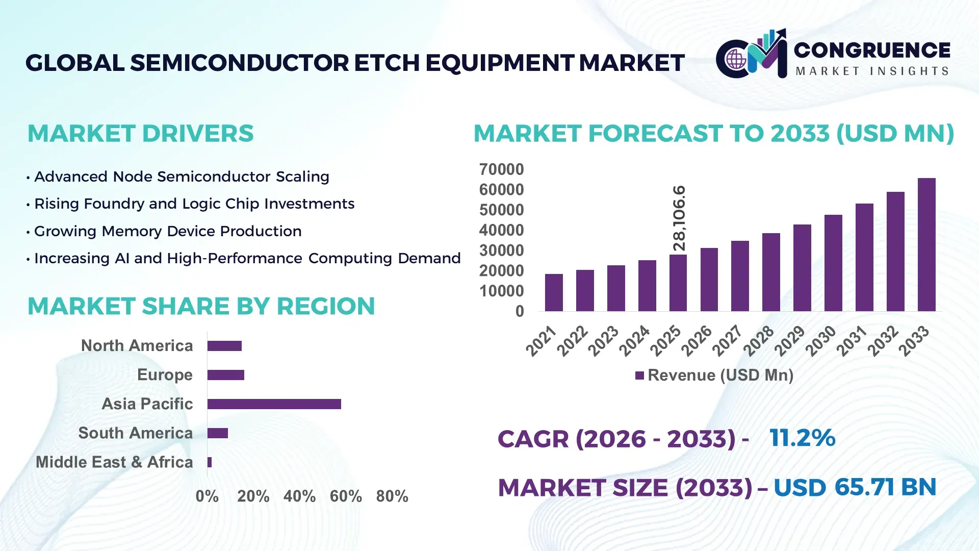
The Global Semiconductor Etch Equipment Market was valued at USD 28106.64 Million in 2025 and is anticipated to reach a value of USD 65712.39 Million by 2033 expanding at a CAGR of 11.2% between 2026 and 2033. Growth is primarily supported by aggressive node scaling below 5 nm and sustained capital expenditure on advanced logic, memory, and heterogeneous integration technologies.
Taiwan stands as the most influential national market for semiconductor etch equipment, supported by a highly concentrated fabrication ecosystem and continuous investments in advanced manufacturing. The country operates more than 20 high-volume semiconductor fabrication plants, with over 65% of installed capacity focused on sub-7 nm and advanced-node production. Annual semiconductor capital spending in Taiwan exceeded USD 36 billion in 2024, enabling widespread deployment of plasma etch, deep reactive ion etch (DRIE), and atomic layer etch systems. Logic integrated circuits account for approximately 55% of etch tool utilization, while memory manufacturing contributes nearly 30%, reflecting strong demand across multiple device architectures and high-volume production environments.
Market Size & Growth: Valued at USD 28106.64 Million in 2025 and projected to reach USD 65712.39 Million by 2033, growing at a CAGR of 11.2%, driven by advanced-node fabrication and rising chip complexity.
Top Growth Drivers: Advanced-node adoption (62%), process yield improvement demand (48%), and AI/HPC chip production expansion (44%).
Short-Term Forecast: By 2028, leading fabs are expected to achieve up to 18% process cost reduction through selective etch optimization and higher chamber utilization rates.
Emerging Technologies: Atomic layer etching, high-aspect-ratio plasma etch, and AI-enabled process control integration.
Regional Leaders: Asia-Pacific projected at USD 37200 Million by 2033 with logic-node leadership; North America at USD 15600 Million driven by domestic fab expansion; Europe at USD 8300 Million supported by automotive and power semiconductor demand.
Consumer/End-User Trends: Foundries and IDMs prioritize high-selectivity, low-damage etch systems for logic, memory, and advanced packaging applications.
Pilot or Case Example: A 2025 advanced-node fab pilot achieved a 22% defect density reduction through atomic layer etch deployment.
Competitive Landscape: Market leader holds approximately 38% share, followed by Applied Materials, Lam Research, Tokyo Electron, Hitachi High-Tech, and KLA.
Regulatory & ESG Impact: Energy-efficiency mandates and fab-level emissions reduction targets accelerate adoption of low-power, gas-optimized etch tools.
Investment & Funding Patterns: Over USD 95 billion in global semiconductor fab investments between 2024–2025, with rising focus on advanced process equipment.
Innovation & Future Outlook: Integration of digital twins, AI-driven predictive maintenance, and co-optimized etch-deposition platforms shaping next-generation fabs.
The Semiconductor Etch Equipment Market serves critical industry sectors including logic devices (approximately 50% of demand), memory fabrication (around 30%), and advanced packaging and power devices (nearly 20%). Recent innovations such as atomic layer etch, real-time plasma diagnostics, and chamber-level AI control are enhancing precision and yield at advanced nodes. Regulatory pressure to reduce greenhouse gas emissions and hazardous gas usage is influencing equipment design and procurement decisions. Regionally, Asia-Pacific leads consumption due to high fab density, while North America and Europe show accelerated growth tied to reshoring initiatives and automotive semiconductor demand. Emerging trends point toward tighter process integration, higher selectivity requirements, and sustained long-term demand from AI, data center, and electrification applications.
The Semiconductor Etch Equipment Market holds strategic relevance as a foundational enabler of advanced semiconductor manufacturing, directly influencing device scaling, yield optimization, and cost efficiency across logic, memory, and power semiconductor production. As device architectures migrate toward sub-5 nm nodes, gate-all-around (GAA) transistors, and 3D NAND structures exceeding 200 layers, etch precision and selectivity have become decisive competitive parameters. Atomic Layer Etching delivers approximately 25% improvement in critical dimension control compared to conventional plasma etch, enabling tighter process windows and reduced defect density. Asia-Pacific dominates in volume due to high fab density, while North America leads in adoption with nearly 48% of advanced-node fabs integrating AI-assisted etch process control systems.
From a strategic pathway perspective, equipment suppliers are increasingly aligning with foundries through co-development models, shortening process qualification cycles by an estimated 15–20%. By 2028, AI-driven process tuning and digital twin deployment are expected to improve tool uptime by nearly 20% and reduce unplanned downtime across advanced fabs. ESG and compliance considerations are also shaping procurement strategies, with firms committing to fluorinated gas abatement improvements such as 35% emission reduction by 2030 and higher recycling rates for process consumables. In 2025, South Korea achieved a 17% reduction in etch-related defect rates through nationwide deployment of AI-enabled plasma monitoring initiatives. Looking forward, the Semiconductor Etch Equipment Market is positioned as a pillar of manufacturing resilience, regulatory alignment, and sustainable growth, supporting long-term innovation across global semiconductor value chains.
Advanced-node scaling remains a primary growth driver for the Semiconductor Etch Equipment Market as manufacturers push toward sub-3 nm logic and vertically stacked memory architectures. Modern logic devices require etch precision at the angstrom level, while 3D NAND production demands uniform etching across more than 200 layers. These requirements have increased demand for atomic layer etch and high-selectivity plasma systems, which can improve pattern fidelity by over 20% compared to legacy approaches. Additionally, advanced packaging techniques such as chiplets and through-silicon vias rely heavily on deep reactive ion etch processes, expanding equipment utilization beyond front-end manufacturing. The cumulative effect is sustained demand for next-generation etch platforms across multiple fabrication stages.
High capital expenditure requirements act as a restraint in the Semiconductor Etch Equipment Market, particularly for smaller foundries and emerging regional fabs. A single advanced-node etch tool can cost several million dollars, and full process qualification may extend beyond 12 months due to stringent yield and reliability standards. These long validation cycles delay return on investment and limit rapid technology adoption. Furthermore, ongoing costs related to specialty gases, maintenance, and skilled labor add operational complexity. In periods of semiconductor demand volatility, these financial and operational burdens can slow procurement decisions and constrain market expansion.
AI-driven manufacturing presents significant opportunities for the Semiconductor Etch Equipment Market by enabling predictive maintenance, adaptive process control, and yield optimization. AI-enabled etch systems can reduce process variability by approximately 15%, improving overall fab efficiency. Advanced packaging growth further expands opportunities, as chiplet-based designs and heterogeneous integration increase demand for precise backside and interconnect etching. Emerging applications in automotive electronics, power devices, and high-performance computing are also driving demand for specialized etch solutions, creating new revenue streams and long-term growth potential for equipment suppliers.
Rising material complexity poses a significant challenge for the Semiconductor Etch Equipment Market as new device structures incorporate novel materials such as high-k dielectrics and compound semiconductors. Achieving selective etching without damaging adjacent layers becomes increasingly difficult, raising process development costs. Simultaneously, stricter environmental regulations targeting greenhouse gas emissions and hazardous chemicals require equipment redesign and additional abatement systems. Compliance investments can increase tool costs and extend development timelines, placing pressure on both manufacturers and end users to balance innovation with regulatory adherence.
Shift Toward Atomic Layer Etch (ALE) for Advanced Nodes: Adoption of atomic layer etch is accelerating as manufacturers move toward sub-5 nm and gate-all-around architectures. Nearly 42% of advanced logic fabs have integrated ALE into at least one critical process step, achieving up to 25% improvement in critical dimension control and around 18% reduction in line-edge roughness compared to conventional plasma etch methods.
Growing Integration of AI-Enabled Process Control: Artificial intelligence and machine learning are increasingly embedded into semiconductor etch equipment to enhance yield and uptime. Around 47% of newly installed etch tools now include AI-assisted diagnostics, enabling predictive maintenance that reduces unplanned downtime by approximately 20% and improves overall equipment effectiveness by nearly 15% within high-volume manufacturing environments.
Rising Demand for High-Aspect-Ratio Etching in 3D Architectures: Expansion of 3D NAND and advanced packaging is driving demand for high-aspect-ratio etch solutions. Memory devices exceeding 200 layers now account for nearly 35% of total etch process steps in memory fabs, with new systems enabling aspect ratios above 80:1 while maintaining etch uniformity improvements of nearly 22% across full wafers.
Increased Focus on Energy Efficiency and Gas Utilization: Sustainability-driven design changes are reshaping equipment specifications, with over 50% of newly deployed etch platforms featuring optimized gas flow and advanced abatement integration. These systems have demonstrated up to 30% reduction in fluorinated gas consumption and nearly 18% lower energy usage per wafer, aligning operational efficiency with tightening environmental compliance requirements.
The Semiconductor Etch Equipment Market is segmented by type, application, and end-user, reflecting the diverse technical requirements across semiconductor manufacturing stages. Product segmentation highlights varying adoption levels of plasma-based, atomic-scale, and specialty etch systems aligned with shrinking geometries and complex materials. Application segmentation is driven by logic, memory, and advanced packaging processes, each demanding different levels of precision, selectivity, and throughput. End-user segmentation underscores the dominance of large-scale foundries and integrated device manufacturers, while research institutes and emerging specialty fabs contribute to niche demand. Across segments, adoption patterns are increasingly influenced by technology node transitions, sustainability mandates, and regional fab expansion strategies, making segmentation analysis critical for strategic planning and investment prioritization.
Plasma etch equipment remains the leading product type, accounting for approximately 48% of total adoption due to its versatility across logic and memory fabrication and compatibility with high-volume manufacturing. Atomic layer etch systems currently represent around 22% of adoption, while deep reactive ion etch tools hold nearly 18%. However, atomic layer etch is the fastest-growing type, expanding at an estimated 14.5% CAGR, driven by demand for angstrom-level precision in sub-5 nm logic and gate-all-around architectures. Plasma etch continues to dominate bulk material removal steps, whereas atomic layer etch is increasingly selected for critical dimension control and selective etching. Other specialized etch types, including wet etch and niche compound semiconductor etch systems, collectively contribute about 12% of adoption, serving power devices and MEMS fabrication.
Logic device manufacturing is the leading application, accounting for roughly 46% of etch equipment utilization, supported by high process complexity and multiple etch steps per wafer. Memory manufacturing, including DRAM and 3D NAND, represents about 34% of application demand, while advanced packaging and power devices collectively account for 20%. Advanced packaging is the fastest-growing application, with an estimated 13.2% CAGR, driven by chiplet architectures, through-silicon vias, and heterogeneous integration. While logic applications remain dominant, adoption in advanced packaging is rising fastest and is expected to exceed 28% of total etch steps by 2033. Memory applications increasingly require high-aspect-ratio etch for structures exceeding 200 layers, intensifying tool utilization.
Foundries constitute the leading end-user segment, representing approximately 52% of total etch equipment adoption due to their focus on advanced-node logic and high wafer throughput. Integrated device manufacturers account for around 33%, while research institutes and specialty fabs together contribute about 15%. Specialty fabs focused on power electronics and compound semiconductors are the fastest-growing end-user group, expanding at an estimated 12.8% CAGR, fueled by electrification, automotive demand, and renewable energy systems. While foundries dominate current usage, adoption among specialty fabs is rising rapidly and is projected to surpass 20% by 2033. IDM adoption remains strong in memory-intensive regions, with over 60% of large IDMs deploying advanced plasma and selective etch systems.
Asia-Pacific accounted for the largest market share at 58% in 2025 however, North America is expected to register the fastest growth, expanding at a CAGR of 12.4% between 2026 and 2033.
Asia-Pacific’s leadership is supported by high fab density, accounting for over 70% of global wafer fabrication capacity, with more than 450 active semiconductor manufacturing facilities. North America holds nearly 22% share, driven by accelerated fab construction and reshoring initiatives, while Europe represents approximately 15%, supported by automotive and power semiconductor demand. South America and the Middle East & Africa collectively contribute around 5%, reflecting early-stage adoption. Regionally, equipment deployment intensity varies significantly, with Asia-Pacific averaging over 1.8 advanced etch tools per 1,000 wafer starts per month, compared to 1.2 in North America and 0.9 in Europe, highlighting differing maturity and investment cycles.
This region accounts for approximately 22% of the global Semiconductor Etch Equipment Market, supported by strong demand from logic, memory, and advanced packaging fabs. Key industries include high-performance computing, AI accelerators, aerospace electronics, and automotive semiconductors. Government-backed manufacturing incentives and tax credits have accelerated fab investments, with over 25 new or expanded facilities announced since 2023. Digital transformation trends include widespread adoption of AI-driven process control, with nearly 50% of newly installed etch tools featuring predictive maintenance capabilities. A leading local equipment supplier expanded its U.S.-based manufacturing footprint in 2025, increasing domestic tool assembly capacity by 30%. Regional buyer behavior shows higher enterprise adoption for mission-critical applications, with fabs prioritizing uptime, automation, and cybersecurity-integrated equipment platforms.
Europe represents around 15% of the Semiconductor Etch Equipment Market, with Germany, France, and the UK accounting for over 65% of regional demand. Automotive electronics, industrial automation, and power semiconductors are the primary application drivers. Regulatory frameworks emphasizing emissions reduction and energy efficiency are influencing procurement, with over 40% of fabs requiring integrated gas abatement and energy-optimized systems. Adoption of selective etch and atomic-scale processes is increasing, particularly for wide-bandgap semiconductors. A European equipment manufacturer reported deployment of next-generation plasma etch tools across multiple automotive-focused fabs, improving process uniformity by 18%. Regional purchasing behavior reflects strong regulatory influence, with buyers favoring explainable, traceable, and compliance-ready etch solutions.
Asia-Pacific is the largest and most mature market, accounting for approximately 58% of global volume, driven by China, Japan, South Korea, and Taiwan. The region hosts more than 70% of global wafer fabrication capacity and leads in both logic and memory production. Manufacturing trends emphasize high-throughput plasma etch and rapid adoption of atomic layer etch for sub-5 nm nodes. Innovation hubs across East Asia are accelerating tool qualification cycles, reducing average process ramp-up time by nearly 20%. A major regional equipment supplier expanded its etch system production lines in 2025 to support rising domestic demand. Buyer behavior is characterized by scale-driven procurement, with fabs prioritizing throughput, yield stability, and cost efficiency to support consumer electronics, mobile devices, and AI-driven applications.
South America holds an estimated 3% share of the global market, with Brazil and Argentina as the primary contributors. Demand is linked to electronics assembly, industrial automation, and early-stage semiconductor initiatives rather than advanced-node fabrication. Infrastructure modernization and trade policies encouraging local electronics manufacturing are gradually increasing equipment imports. Government incentives focused on technology parks and industrial diversification have supported pilot-scale semiconductor projects. Regional suppliers are increasingly collaborating with international equipment vendors to build local servicing and integration capabilities. Buyer behavior in this region reflects application-driven demand, with emphasis on cost-effective, flexible etch tools aligned to consumer electronics and media-related device production.
The Middle East & Africa region accounts for roughly 2% of the Semiconductor Etch Equipment Market, led by the UAE, Israel, and South Africa. Demand is driven by industrial electronics, defense systems, energy monitoring devices, and research fabs. Technological modernization initiatives and trade partnerships have supported limited but strategic equipment deployment. Regional regulations emphasize technology transfer and local value creation. A regional technology hub expanded its semiconductor research facilities in 2024, increasing etch tool utilization by over 25% year-on-year. Buyer behavior varies widely, with demand concentrated among government-backed projects and research institutions prioritizing flexibility, reliability, and long-term service support.
China – 28% market share: High production capacity supported by large-scale domestic fabs and sustained investment in logic and memory manufacturing infrastructure.
United States – 20% market share: Strong end-user demand driven by advanced-node logic, AI-focused chips, and government-backed manufacturing expansion programs.
The Semiconductor Etch Equipment market exhibits a moderately consolidated competitive structure, characterized by a limited number of global technology leaders and a broader base of specialized regional and niche players. More than 30 active competitors operate worldwide, spanning full-line equipment manufacturers, process-specific specialists, and emerging technology providers focused on atomic-scale and AI-enabled etch solutions. The top five companies collectively account for approximately 75% of total equipment installations, reflecting high entry barriers driven by capital intensity, intellectual property depth, and long customer qualification cycles that often exceed 9–12 months.
Competition is primarily based on process performance, yield enhancement, tool uptime, and compatibility with advanced nodes below 5 nm. Strategic initiatives increasingly include long-term co-development agreements with foundries, joint R&D programs for gate-all-around and 3D NAND architectures, and accelerated product refresh cycles. In the last two years, over 40% of leading players have launched next-generation etch platforms integrating AI-based diagnostics, achieving reported uptime improvements of 15–20%. Partnerships with gas suppliers and abatement technology firms are also shaping differentiation, as environmental compliance and process efficiency gain importance. Overall, innovation intensity, customer lock-in through process integration, and regional manufacturing footprints remain decisive competitive factors.
Applied Materials
Lam Research
Tokyo Electron
Hitachi High-Tech
KLA
SPTS Technologies
Plasma-Therm
ULVAC
The Semiconductor Etch Equipment Market is being reshaped by a suite of advanced technologies that address increasingly demanding process requirements in modern semiconductor fabrication. Atomic layer etching (ALE) has emerged as a critical technology for sub-5 nm and beyond, enabling angstrom-level material removal with selective precision. Adoption of ALE has reached approximately 22% of newly installed etch platforms in advanced logic and memory fabs, driven by its ability to reduce line-edge roughness by up to 25% compared with legacy plasma etch techniques. High-aspect-ratio etching systems capable of handling aspect ratios above 80:1 are becoming essential for 3D NAND and advanced packaging structures, where uniformity across complex topographies influences device performance and yield.
Digital transformation initiatives have accelerated the integration of artificial intelligence and machine learning within etch systems. Nearly half of all new tools deployed in leading fabs include AI-enabled process control modules that monitor chamber conditions, adapt plasma parameters in real time, and predict maintenance needs. These AI enhancements are reducing unplanned downtime by upwards of 18% and improving first-pass yield consistency across multi-step etch sequences. Real-time plasma diagnostics, including optical emission spectroscopy and mass spectrometry integration, further strengthen process repeatability and defect reduction efforts.
In addition to core etch advancements, there is significant focus on environmental and safety technologies within etch equipment. Next-generation gas abatement and recycling modules integrated into etch platforms are reducing fluorinated gas usage by around 30% while lowering energy consumption by approximately 15%. Materials innovation is also expanding, with specialty etch chemistries tailored for compound semiconductors, wide-bandgap materials, and sensitive high-k dielectrics. As chip architectures become more heterogeneous, co-optimized etch and deposition tools are gaining traction to simplify process integration and enhance throughput, solidifying technology leadership as a key differentiator in the Semiconductor Etch Equipment Market.
• In October 2025, Applied Materials launched the Centura™ Xtera™ Epi system, a production-oriented integrated pre-clean and etch platform designed for 2nm gate-all-around transistor fabrication, significantly improving epitaxial layer uniformity across advanced logic lines. (knowledge-sourcing.com)
• In February 2025, Lam Research unveiled its Akara® plasma conductor etch tool, providing enhanced precision control for next-generation gate-all-around logic and 3D NAND applications, enabling tighter process control with reduced defect rates.
• In 2024, Tokyo Electron expanded its dry etch system production capacity in Hokkaido, Japan to meet rising memory fab demand for 300+ layer 3D NAND structures, boosting regional supply capabilities.
• In October 2024, Tokyo Electron reported development of a cryogenic etching process that reduced CO₂ emissions by approximately 80% compared with conventional etch methods, supporting “digital and green transformation” initiatives in etch processes.
The scope of the Semiconductor Etch Equipment Market Report encompasses a comprehensive analysis of market segments across types of etching technologies, key application domains, geographic regions, and end-user industries. Within the type segment, detailed coverage includes traditional plasma etch, high-aspect-ratio deep reactive ion etch, and emerging atomic layer etch systems, highlighting adoption patterns, precision capabilities, and suitability for complex process nodes. Application analysis examines logic device fabrication, memory processes including 3D NAND and DRAM, and advanced packaging etch steps, each requiring tailored etch solutions to address pattern fidelity, sidewall integrity, and throughput demands.
Geographic segmentation covers major regional markets such as Asia-Pacific, North America, Europe, South America, and Middle East & Africa, offering insight into regional manufacturing intensity, infrastructure maturity, and consumer behavior trends influencing etch tool procurement and deployment. Technology focus areas within the report include AI-enabled process control integration, real-time plasma diagnostics, sustainability-driven designs with optimized gas usage and energy efficiency, and hybrid etch/deposition platforms that address co-optimization opportunities for next-generation devices.
The end-user section addresses foundries, integrated device manufacturers, research and academic fabs, and specialty semiconductor fabs, detailing equipment utilization rates, technology upgrade cycles, and industry-specific process requirements. Emerging or niche segments such as compound semiconductor etching for SiC and GaN devices, MEMS and photonics etch requirements, and bespoke etch solutions for wide-bandgap materials are also examined to capture forward-looking market dynamics. Taken together, the report provides decision-makers with a structured, data-informed overview of the full breadth of the Semiconductor Etch Equipment landscape, enabling strategic planning for investment, technology adoption, and competitive positioning.
| Report Attribute/Metric | Report Details |
|---|---|
|
Market Revenue in 2025 |
USD V2025 Million |
|
Market Revenue in 2033 |
USD V2033 Million |
|
CAGR (2026 - 2033) |
11.2% |
|
Base Year |
2025 |
|
Forecast Period |
2026 - 2033 |
|
Historic Period |
2021 - 2025 |
|
Segments Covered |
By Types
By Application
By End-User
|
|
Key Report Deliverable |
Revenue Forecast, Growth Trends, Market Dynamics, Segmental Overview, Regional and Country-wise Analysis, Competition Landscape |
|
Region Covered |
North America, Europe, Asia-Pacific, South America, Middle East, Africa |
|
Key Players Analyzed |
Applied Materials, Lam Research, Tokyo Electron, Hitachi High-Tech, KLA, SPTS Technologies, Plasma-Therm, ULVAC |
|
Customization & Pricing |
Available on Request (10% Customization is Free) |


