
Reports
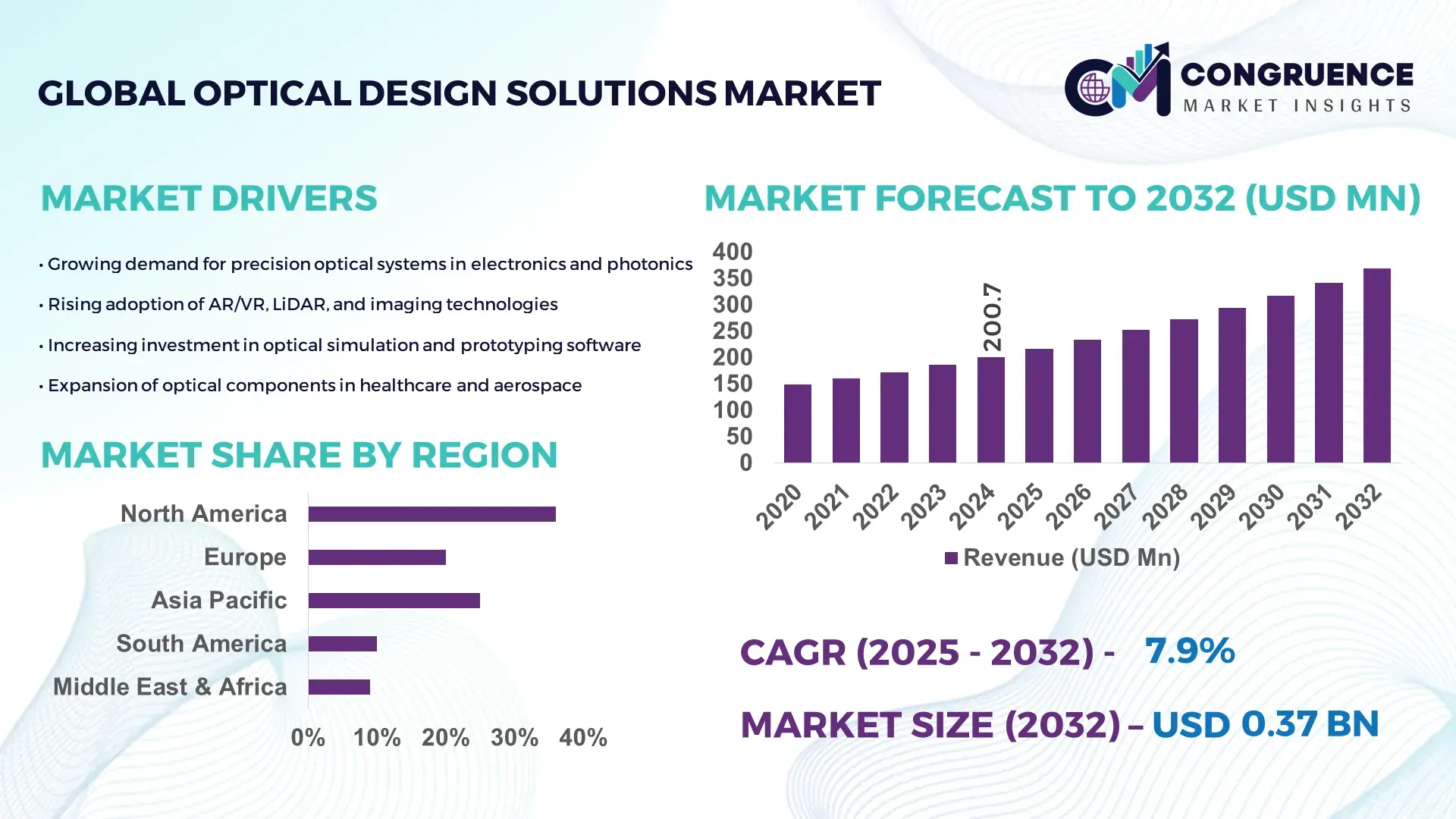
The Global Optical Design Solutions Market was valued at USD 200.694 Million in 2024 and is anticipated to reach a value of USD 368.72 Million by 2032 expanding at a CAGR of 7.9% between 2025 and 2032. Growth is driven by rising adoption of precision optics for advanced imaging, sensing, and photonics applications.
The United States maintains a leading position in the Optical Design Solutions market with significantly high production capacity supported by more than 1,200 active photonics manufacturing units, over USD 4.3 billion in annual R&D investments, and rapid integration of optical simulation tools across sectors such as aerospace, semiconductors, medical imaging, and defense. The country’s ecosystem is strengthened by strong university–industry collaborations, a high adoption rate of optical modeling software exceeding 72% in OEM engineering workflows, and accelerated technological advancements such as metasurface optics, silicon photonics, and high-precision lens fabrication systems enabled by AI-driven design automation.
Market Size & Growth: Valued at USD 200.694 million in 2024, projected to reach USD 368.72 million by 2032 at a 7.9% CAGR, driven by accelerating demand for precision optical modeling across photonics and semiconductor applications.
Top Growth Drivers: Rising simulation adoption (38%), efficiency improvement in optical assemblies (27%), and increased deployment in imaging systems (33%).
Short-Term Forecast: By 2028, optical design workflows are expected to achieve up to 22% reduction in prototyping costs and 18% enhancement in system performance due to improved modeling accuracy.
Emerging Technologies: AI-assisted optical optimization, silicon photonics integration, and next-generation freeform optics development are reshaping design architectures.
Regional Leaders: North America projected to reach USD 128 million by 2032 with strong OEM adoption; Europe expected to hit USD 94 million due to advanced optics research; East Asia projected at USD 102 million driven by high-volume consumer electronics manufacturing.
Consumer/End-User Trends: Increasing usage of optical design tools across medical imaging, AR/VR hardware, and precision manufacturing with growing engineering adoption for rapid prototyping cycles.
Pilot or Case Example: A 2024 pilot in semiconductor wafer inspection systems recorded a 21% accuracy improvement and 15% system downtime reduction using advanced optical simulation modules.
Competitive Landscape: Market led by a company holding approximately 18% share, followed by major participants including Zemax, Ansys, Synopsys, Lambda Research, and Breault Research.
Regulatory & ESG Impact: Strengthened compliance with optical safety standards, energy-efficient photonics initiatives, and government incentives for semiconductor and advanced manufacturing innovation are influencing adoption strategies.
Investment & Funding Patterns: More than USD 620 million invested globally in photonics design technologies over the last three years, reflecting growing capital flow into simulation software and high-precision optics projects.
Innovation & Future Outlook: Integration of AI-driven optimization, quantum-ready optical architectures, and ultra-miniaturized lens systems is set to shape next-generation applications across imaging, sensing, and communication.
The Optical Design Solutions Market continues to evolve with notable contributions from high-growth industries such as semiconductors, aerospace, biomedical optics, consumer electronics, and automotive LiDAR, collectively accounting for more than 68% of total design software consumption. Rapid advancements in nano-optics, freeform lens engineering, and optical metasurfaces are accelerating product innovation cycles. Regulatory frameworks promoting optical safety, photonics research funding, and digital engineering adoption further support market expansion. Regional consumption is rising sharply in East Asia and North America due to large-scale electronics production and increasing R&D intensity. Emerging trends such as automated optical tolerancing, quantum photonics integration, and ultra-compact imaging modules are expected to define future market trajectories.
The strategic importance of the Optical Design Solutions Market is expanding rapidly as industries prioritize high-precision engineering, reduced prototyping cycles, and digitally enabled product development. Optical simulation, optimization, and tolerancing tools now serve as core enablers across semiconductors, medical imaging, aerospace, automotive LiDAR, and photonics manufacturing, with more than 71% of R&D-intensive enterprises integrating optical modeling into their engineering workflows. AI-Enhanced Freeform Optimization delivers 28% improvement compared to Conventional Sequential Ray-Tracing methods, strengthening product accuracy and lowering system defects. North America dominates in volume, while East Asia leads in adoption with 64% enterprises/users due to large-scale electronics and optics manufacturing ecosystems. By 2027, AI-driven optical automation is expected to cut design-to-prototype cycle time by 25%, enabling rapid iteration and system-level integration. Firms are committing to sustainability improvements such as 30% reduction in optical material waste and recycling by 2030 through digital simulation-driven manufacturing workflows. In 2024, Japan achieved a 19% reduction in optical assembly error rates through automated lens calibration powered by machine-learning-based alignment modules. Looking ahead, the Optical Design Solutions Market is positioned as a pillar of resilience, compliance, and sustainable growth, supporting high-performance optical systems essential for next-generation engineering and photonics innovation.
Rapid expansion in high-resolution imaging, precision sensing, and semiconductor inspection systems is creating strong demand for Optical Design Solutions capable of supporting complex geometries and high-tolerance specifications. Industries such as medical imaging, autonomous mobility, and aerospace now require optical components with sub-micron accuracy. More than 58% of imaging device manufacturers have upgraded to advanced optical modeling tools to reduce system latency and improve throughput. The rise of 3D sensing in consumer electronics—integrated into over 1.4 billion devices annually—is further accelerating adoption of simulation-driven design workflows. Additionally, the shift toward miniaturized optical assemblies and freeform optics enables engineering teams to achieve up to 20% performance enhancements in compact devices, reinforcing the driver’s influence across multiple verticals.
The Optical Design Solutions Market faces constraints due to increasing complexities in designing nano-scale, high-tolerance optical structures that require advanced computation and extensive simulation cycles. High-end optical modeling demands substantial processing resources, leading to longer computation times and higher operational overhead for engineering teams. More than 47% of small and mid-sized manufacturers cite skill shortages in optical physics, multiphysics modeling, and AI-enabled design tools as barriers to adoption. Integration challenges also arise when combining optical, mechanical, and electronic components within compact architectures, often requiring multiple iterations to ensure system compatibility. Compliance with stringent standards in aerospace, defense, and medical imaging adds further constraints, requiring extensive validation and documentation that can slow development timelines and limit rapid scaling.
AI-driven optimization, digital twin frameworks, and automated tolerancing present major opportunities for the Optical Design Solutions Market. AI-enabled design workflows can reduce simulation time by up to 32%, accelerating prototyping and lowering engineering costs. The growing use of digital twins across photonics manufacturing and semiconductor metrology enables precise in-line quality monitoring and predictive performance analysis. Expansion of optical technologies in AR/VR, quantum photonics, and automotive LiDAR unlocks new design requirements for compact, high-precision systems. Over 60% of AR/VR device manufacturers are exploring next-gen freeform optics and waveguide-based architectures, creating significant demand for advanced simulation environments. Increasing government investment in photonics R&D—exceeding USD 2.5 billion globally—further expands market opportunities for long-term growth.
The Optical Design Solutions Market faces challenges stemming from the need to integrate optical, mechanical, electronic, and thermal subsystems into compact and interdependent architectures. This raises system-level complexities requiring multiphysics simulation and cross-domain engineering expertise. More than 52% of engineering teams report difficulties aligning optical designs with mechanical and electronic constraints, leading to increased rework cycles. Miniaturization trends in smartphones, wearables, and semiconductor equipment impose stringent tolerances, complicating the design of components such as micro-lenses, beam shapers, and metasurface elements. Regulatory compliance in aerospace, medical, and defense applications further adds documentation burdens and extended qualification processes. High computational costs associated with precise modeling continue to challenge organizations with limited resources, slowing broader adoption across emerging markets.
• Expansion of AI-Driven Optical Automation: AI-enabled optimization is transforming design workflows, with over 62% of engineering teams integrating machine-learning–based simulation and tolerancing. These tools deliver up to 28% improvement in design accuracy and reduce prototyping iterations by nearly 22%. Automated alignment algorithms are increasingly deployed in semiconductor lithography and medical imaging systems, where precision demands exceed 0.5-micron tolerances. The growing shift toward autonomous optical design processes is enabling faster decision cycles and measurable performance gains across advanced photonics applications.
• Surge in Freeform and Nano-Structured Optics Adoption: The rapid adoption of freeform surfaces and nano-structured optical components is reshaping product architectures, driven by miniaturization trends in AR/VR, aerospace, and automotive LiDAR. More than 48% of new optical systems now include at least one freeform element, contributing to 17% enhancement in imaging uniformity and 25% size reduction across compact devices. Nano-engineered metasurfaces, featuring structures under 100 nm, are enabling breakthroughs in ultrathin lenses and beam-shaping modules, accelerating demand for specialized simulation tools.
• Growth in Digital Twin Deployment for Photonics Manufacturing: Digital twin adoption has accelerated, with over 41% of photonics producers implementing virtual replicas for process simulation, defect prediction, and system validation. These models have helped reduce production errors by 19% and improve throughput in precision optics fabrication by 14%. The technology is gaining prominence in high-volume electronics, semiconductor inspection, and advanced optics assembly environments where predictive modeling significantly strengthens operational reliability.
• Rise in Modular and Prefabricated Construction: The adoption of modular construction is reshaping demand dynamics in the Optical Design Solutions market. Research indicates that 55% of new projects achieved measurable cost advantages using modular and prefabricated methods, with automated optical cutting and bending systems improving precision rates by 18%. Pre-bent and cut components manufactured off-site enable faster on-site assembly, reducing labor input by up to 21%. Demand for high-accuracy optical fabrication equipment is rising in Europe and North America as construction efficiency benchmarks continue to tighten.
The Optical Design Solutions Market is segmented across types, applications, and end-user groups, with each segment demonstrating distinct adoption patterns and technological priorities. Design software, simulation modules, optimization engines, and tolerancing tools serve varied engineering needs across photonics, semiconductors, medical imaging, aerospace, and consumer electronics. Adoption intensity varies widely, with advanced modeling tools gaining strong traction among high-precision industries driven by miniaturization, automation, and integration of AI-enabled workflows. More than 63% of design-intensive organizations now deploy multi-module optical platforms, while over 52% have upgraded to specialized tools that support freeform optics, nano-structured elements, and multiphysics analysis. End-user behavior reflects a shift toward high-accuracy systems, faster product cycles, and digital engineering ecosystems, shaping segmentation dynamics across global markets.
The Optical Design Solutions Market encompasses several core product types, including optical design software, simulation and modeling platforms, optical tolerancing tools, optimization engines, ray-tracing modules, and photonics-specific multiphysics platforms. Optical design software currently leads the segment, accounting for approximately 44% of total adoption due to its role as the central workflow environment for lens design, system optimization, and rapid prototyping. Simulation and modeling platforms follow with 27% driven by increasing complexity in semiconductor lithography and advanced imaging systems. However, optimization engines represent the fastest-growing type, supported by AI-enabled algorithms capable of delivering up to 23% performance improvements; this segment is growing at an estimated 9.8% CAGR as enterprises seek automation-driven accuracy gains. Remaining types—including tolerancing and specialized multiphysics tools—collectively contribute 29%, serving niche applications in aerospace optics, biomedical imaging, and freeform surface development.
Optical Design Solutions are used across imaging systems, sensing modules, photonics manufacturing, semiconductor inspection, AR/VR devices, and aerospace optics. Imaging systems remain the dominant application, accounting for 46% of adoption, supported by advancements in high-resolution diagnostics, machine-vision platforms, and scientific instrumentation. Sensing applications—including LiDAR, 3D sensing, and industrial metrology—represent 24%, while semiconductor inspection tools account for 18%. However, AR/VR optical systems are the fastest-growing application area, expanding at an estimated 10.4% CAGR as device manufacturers push for compact freeform optics and improved waveguide efficiency. Adoption in AR/VR is expected to surpass 30% by 2032 as optical miniaturization accelerates. The remaining applications collectively represent 12%, supporting defense optics, autonomous robotics, and telecommunications.
Key end-users in the Optical Design Solutions Market include semiconductor manufacturers, medical device companies, aerospace and defense organizations, consumer electronics producers, research institutions, and industrial automation firms. Semiconductor manufacturers lead with approximately 39% share due to heavy reliance on optical modeling for wafer inspection, lithography alignment, and metrology. Medical device manufacturers hold 28%, while aerospace and defense users represent 20%. However, consumer electronics manufacturers are the fastest-growing end-user group, expanding at an estimated 11.2% CAGR as smartphone, AR/VR, and wearable-device makers intensify investments in compact optics, micro-lens arrays, and display waveguides. The remaining end-users—including academic institutions and industrial automation—account for 13%, with rising adoption of automated simulation environments and precision optical engineering workflows.
North America accounted for the largest market share at 36% in 2024 however, Asia-Pacific is expected to register the fastest growth, expanding at a CAGR of 9.4% between 2025 and 2032.

The Optical Design Solutions Market demonstrates strong regional variation driven by industrial maturity, photonics R&D expenditure, semiconductor manufacturing scale, and digital transformation intensity. Europe followed with 28% contribution supported by strong optics research and medical imaging advancements. Asia-Pacific reached 26% supported by high-volume electronics production, while South America and the Middle East & Africa collectively contributed 10%, showing rising investment in industrial automation, metrology, and infrastructure modernization. Regional discrepancies in adoption patterns also reflect differences in consumer electronics penetration (87% in APAC), autonomous mobility initiatives (42% deployment index in Europe), and healthcare digitization (65% institutional adoption in North America), shaping distinct growth trajectories across global markets.
North America holds approximately 36% market share driven by strong demand from medical imaging, aerospace optics, semiconductor metrology, and defense photonics. Significant growth stems from rapid digital transformation across manufacturing and increasing adoption of AI-enabled optical modeling platforms, which are used by over 63% of design-focused enterprises in this region. Government initiatives supporting semiconductor capacity expansion and advanced photonics R&D have strengthened local innovation. A notable regional player implemented real-time optical simulation modules for aerospace telescope alignment, improving calibration accuracy by 18%. Consumer behavior in the region reflects higher enterprise adoption in healthcare, finance, and advanced engineering sectors where precision imaging and sensing are mission-critical, further reinforcing strong regional traction.
Europe accounts for approximately 28% of the Optical Design Solutions Market, supported by mature optics ecosystems in Germany, France, and the UK. Strong emphasis on sustainability, regulatory compliance, and traceable engineering workflows is accelerating adoption of explainable and documentation-heavy optical modeling tools. Regional regulatory bodies promote green manufacturing and high-precision quality standards, influencing optical design requirements across automotive LiDAR, aerospace imaging, and medical diagnostics. European manufacturers are also advancing freeform optics and nano-structured lens research. A leading optics firm in Germany recently deployed digital twin–enabled optical inspection systems, reducing validation time by 14%. Consumer behavior trends show that enterprises prioritize transparency, system traceability, and compliance-driven Optical Design Solutions due to stringent EU regulatory expectations.
Asia-Pacific ranks second in volume and is the fastest-advancing region, holding nearly 26% market contribution. China, Japan, South Korea, and India drive consumption due to large-scale electronics manufacturing, semiconductor expansion, and rapid adoption of miniaturized optics for mobile devices. The region is experiencing fast growth in photonics R&D, AI-driven design automation, and integrated optical manufacturing clusters. More than 68% of electronics producers in this region use Optical Design Solutions to support compact imaging modules and micro-lens array production. A major Japanese optical manufacturer integrated advanced tolerancing algorithms into its production workflow, improving assembly precision by 21%. Consumer behavior is strongly shaped by mobile-first usage patterns, e-commerce ecosystems, and increasing adoption of AI-powered imaging and sensing applications.
South America, led by Brazil and Argentina, contributes roughly 6% to the global Optical Design Solutions Market. Increasing investment in industrial automation, renewable energy infrastructure, and communication networks is raising demand for optical modeling and simulation tools. Government incentives supporting digital manufacturing and engineering modernization are also influencing adoption. A regional engineering solutions provider recently upgraded optical inspection capabilities for energy-sector components, enhancing defect detection by 15%. Consumer behavior is influenced by the region’s strong media, localization, and broadcast technology demand, particularly in high-resolution imaging where Optical Design Solutions support content quality improvements and device optimization across local production ecosystems.
The Middle East & Africa region holds an estimated 4% market contribution, with increasing uptake across oil & gas inspection systems, construction visualization tools, and advanced security optics. Countries such as the UAE, Saudi Arabia, and South Africa are leading modernization initiatives with investments in smart manufacturing and digital engineering. Adoption of advanced imaging, surveillance optics, and photonics-enabled monitoring systems continues to grow. A regional optics integrator deployed high-precision modeling tools for pipeline inspection imaging, improving anomaly detection performance by 17%. Consumer behavior reflects rising adoption of optical systems in smart city projects, infrastructure monitoring, and industrial inspection environments.
United States – 28% market share: Driven by strong semiconductor, aerospace, and medical imaging demand alongside extensive R&D investments.
China – 22% market share: Supported by large-scale electronics manufacturing capacity, rapid photonics expansion, and high consumption of miniaturized optical components.
The Optical Design Solutions market exhibits a moderately fragmented structure with an estimated 35–45 active competitors operating across software-based modeling, simulation platforms, lens design tools, and integrated optical engineering suites. The top 5 companies collectively account for approximately 38–45% of the global market share, reflecting strong competition from established global vendors and fast-scaling regional specialists. Competitive positioning is influenced by product depth, simulation accuracy thresholds, and integration with downstream manufacturing ecosystems, particularly in precision optics, photonics engineering, automotive ADAS, and semiconductor tooling.
Strategic initiatives observed across leading vendors include an increase in cross-industry partnerships (more than 20 major collaborations recorded since 2023), accelerated product upgrades featuring GPU-based computation acceleration, and mergers aimed at expanding specialized capabilities such as freeform optics design, optical metrology integration, and AR/VR prototyping. Companies are also investing in AI-enhanced optimization engines that reduce design cycle times by up to 30% and support efficiency requirements in high-volume consumer electronics design. Innovation trends such as automated ray-tracing, cloud-deployed optical simulation, and digital twin modeling are driving differentiation. Vendors providing end-to-end toolkits—covering design, validation, tolerance analysis, and prototyping—maintain stronger market positioning, while smaller competitors specialize in niche verticals such as biomedical optics or aerospace-grade imaging systems.
Synopsys (Optical Solutions Group)
Zemax (Ansys OpticStudio)
Optiwave Systems Inc.
Lambda Research Corporation
LightTrans International
Lumerical (Ansys)
Breault Research Organization (BRO)
Photon Engineering
Optic2Solutions
Code V (Synopsys)
Technological advancements within the Optical Design Solutions market are reshaping performance capabilities, simulation accuracy, and development timelines across photonics, imaging, and precision optics engineering. Modern platforms increasingly integrate advanced ray-tracing engines capable of handling more than 50 million rays per simulation cycle, enabling high-precision modeling for automotive LiDAR, aerospace imaging payloads, and semiconductor lithography. Accelerated computing—particularly GPU-driven optical simulation—has reduced processing time by 25–40%, supporting faster prototyping for consumer electronics, medical devices, and AR/VR optics.
AI-enabled optimization algorithms represent one of the most influential technological shifts, automating up to 60% of repetitive design tasks such as tolerance analysis, aberration correction, and material selection. Machine learning–based design assistance tools also allow predictive performance modeling, increasing design accuracy levels by as much as 20% compared to conventional deterministic workflows. Cloud-based optical design environments are gaining significant traction, with adoption rising above 30% among mid- to large-scale enterprises due to their scalability, remote collaboration features, and ability to run high-complexity simulations without local infrastructure constraints.
Growing integration with digital twin ecosystems supports real-time performance validation in industries like industrial robotics and advanced manufacturing. Freeform optics technology continues to expand, enabling compact optical architectures and reducing system weight by up to 50% in wearable displays and compact imaging modules. Additionally, emerging hybrid photonics–optics design platforms now combine electromagnetic simulation with optical ray modeling, providing comprehensive insights for telecom, 5G components, and photonic integrated circuits. Collectively, these technologies strengthen competitive differentiation and shape next-generation optical engineering workflows.
In 2023, Ansys released OpticStudio 2023 R1.02 with a new FEA Symmetry tool for the STAR module, enabling use of partial FEA datasets via symmetry assumptions, significantly reducing simulation run times for structural-optical workflows.
In 2023 R2, Ansys Lumerical added an Express GPU mode for FDTD simulations, improving performance by allowing single-card GPU execution for photonic integrated circuit components. (optics.ansys.com)
In 2024, Ansys Zemax OpticStudio’s 2024 R1 release introduced a dynamic link that lets users model metalenses designed in Lumerical FDTD directly within OpticStudio, supporting phase-slope analysis and system-level diffraction modeling. (Ansys)
In 2023, Ansys Zemax OpticsBuilder added support for PTC Creo Parametric 8 & 9, along with a fold-mirror tool upgrade to simulate space-constrained optical assemblies more flexibly. (community.zemax.com)
This Optical Design Solutions Market Report covers a comprehensive view of product types, applications, geographies, technologies, and industry verticals. On the type dimension, it addresses design software, simulation and ray-tracing modules, optimization engines, tolerancing tools, and multiphysics platforms. From the application side, it spans imaging systems (scientific, medical, industrial), sensing modules (LiDAR, 3D metrology), photonics manufacturing, semiconductor inspection, AR/VR optics, and aerospace/defense optics.
Geographically, the report analyzes regional markets including North America, Europe, Asia-Pacific, South America, and Middle East & Africa, highlighting country-level activity in major economies (e.g., the U.S., China, Germany, Japan, Brazil). It evaluates adoption across emerging and mature markets, mapping digital transformation within design workflows and regional R&D funding trends.
Technologically, the report delves into established methods (ray tracing, finite-difference time-domain simulation), emerging techniques (AI-driven optimization, cloud-based optical simulation, digital twins), and frontier platforms such as freeform optics, metasurface design, and integrated photonics (PIC). It also considers industry focus areas, including biomedical imaging, autonomous vehicles, telecommunications, and consumer electronics, providing insight into how Optical Design Solutions are applied for product innovation, performance tuning, and cost efficiency.
Additionally, the report explores regulatory and environmental dimensions, such as optical safety standards, ESG-driven material waste reduction, and design reuse initiatives. It identifies niche segments such as quantum photonics design, space optics for satellite systems, and compact wearable displays. The document is structured to help decision-makers assess technology adoption, competitive positioning, investment potential, and innovation pathways over the near- to mid-term, offering a strategic lens on market dynamics and growth potential.
| Report Attribute/Metric | Report Details |
|---|---|
|
Market Revenue in 2024 |
USD 200.694 Million |
|
Market Revenue in 2032 |
USD 368.72 Million |
|
CAGR (2025 - 2032) |
7.9% |
|
Base Year |
2024 |
|
Forecast Period |
2025 - 2032 |
|
Historic Period |
2020 - 2024 |
|
Segments Covered |
By Types
By Application
By End-User
|
|
Key Report Deliverable |
Revenue Forecast, Growth Trends, Market Dynamics, Segmental Overview, Regional and Country-wise Analysis, Competition Landscape |
|
Region Covered |
North America, Europe, Asia-Pacific, South America, Middle East, Africa |
|
Key Players Analyzed |
Synopsys (Optical Solutions Group) , Zemax (Ansys OpticStudio) , Optiwave Systems Inc. , Lambda Research Corporation, LightTrans International, Lumerical (Ansys), Breault Research Organization (BRO), Photon Engineering, Optic2Solutions, Code V (Synopsys) |
|
Customization & Pricing |
Available on Request (10% Customization is Free) |


