
Reports
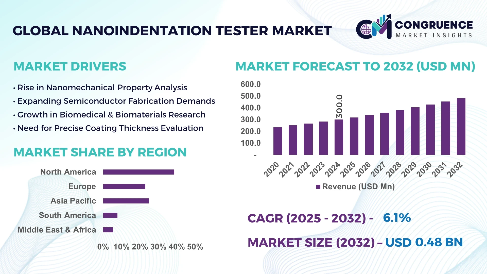
The Global Nanoindentation Tester Market was valued at USD 300 Million in 2024 and is anticipated to reach a value of USD 481.8 Million by 2032 expanding at a CAGR of 6.1% between 2025 and 2032.
The United States leads the global Nanoindentation Tester Market, with robust production infrastructure and consistent investment in nano-scale mechanical characterization tools. The country hosts several advanced research facilities and laboratories specializing in materials testing. U.S. manufacturers have significantly increased automation in production processes, enabling high-throughput nanoindentation analysis. Technological advancements in integration with atomic force microscopy (AFM) and scanning probe techniques further enhance the nation’s dominance in this domain.
The Nanoindentation Tester Market serves critical applications across industries such as aerospace, automotive, biomedical, semiconductors, and advanced materials research. Aerospace and automotive sectors are major contributors due to their growing reliance on high-performance materials requiring precise mechanical characterization at the nanoscale. Recent product innovations include nanoindentation systems integrated with in-situ imaging and real-time data analytics, improving result accuracy and usability. Regulatory drivers include stringent international standards for nanomaterials characterization, while environmental factors such as the push for sustainable materials are accelerating the adoption of nanoindentation technologies. Economically, rising R&D budgets in nanotechnology and material science have fueled regional consumption, especially in North America, Europe, and parts of Asia-Pacific. The market is also witnessing a surge in demand for portable and automated nanoindentation systems. Emerging trends point to hybrid testing platforms and machine-learning-based result interpretation, enhancing the relevance of nanoindentation tools in materials innovation and failure analysis.
Artificial Intelligence (AI) is driving a paradigm shift in the Nanoindentation Tester Market by improving precision, process automation, and data analysis capabilities. AI-powered systems enable real-time feedback during indentation, reducing errors and enhancing consistency in mechanical property measurements. AI integration has led to a 25–35% reduction in test cycle times through automated load-displacement curve interpretation, eliminating the need for manual analysis. Additionally, deep learning models are being employed to classify materials and identify anomalies in microstructure with high accuracy, streamlining material validation processes across R&D laboratories and manufacturing facilities.
In advanced nanoindentation testers, AI algorithms continuously optimize testing parameters—such as loading rate, hold time, and unloading profile—based on real-time material behavior. This has substantially improved the reliability of results, especially for heterogeneous and composite materials. AI also supports predictive maintenance of testing equipment by monitoring mechanical wear patterns and generating alerts before system failures, thereby minimizing operational downtime. These intelligent systems are now being deployed widely in industrial and academic research settings to improve throughput and scalability of materials testing. As the demand for high-performance materials increases, AI’s role in the Nanoindentation Tester Market is expanding, enabling advanced capabilities such as adaptive testing environments and autonomous experimentation.
“In February 2025, a U.S.-based laboratory deployed an AI-integrated nanoindentation system that reduced manual data processing time by 80% and improved indentation precision by 22% in heterogeneous polymer composite testing, marking a significant milestone in smart materials analysis.”
The Nanoindentation Tester Market is influenced by technological innovation, cross-sector demand for material characterization, and evolving standards in nanomechanical testing. The increasing need for precision in evaluating thin films, biomaterials, polymers, and metals is creating sustained demand for advanced nanoindentation systems. Market dynamics are also shaped by the shift toward automation and AI-enabled systems, as well as growing investment in nanotechnology research across public and private sectors. Additionally, collaborations between equipment manufacturers and research institutions are accelerating product development cycles and innovation. These factors, along with regional policy support and rising adoption in academic and industrial laboratories, are driving a dynamic and competitive global marketplace.
One of the primary growth drivers in the Nanoindentation Tester Market is the increasing integration of nanoindentation modules with broader multi-functional platforms. These advanced instruments can now simultaneously perform mechanical, electrical, and thermal characterization of materials. For instance, combined nanoindentation and atomic force microscopy (AFM) systems are now capable of delivering simultaneous topographical and mechanical data at sub-nanometer resolution. This integration significantly enhances the utility of nanoindentation in sectors like semiconductors and biomedical research. It reduces the need for multiple instruments, shortens testing timeframes, and delivers more holistic datasets, thereby increasing adoption rates among high-precision industries.
A key restraint in the Nanoindentation Tester Market is the high complexity and cost associated with the calibration and maintenance of these instruments. Ensuring sub-micron precision requires frequent recalibration using certified reference materials and environmental stability. Inaccuracies due to minor thermal drift, vibration, or tip degradation can compromise data validity, necessitating sophisticated control systems and skilled technicians. Many institutions, especially in developing regions, face operational challenges due to a lack of expertise or resources to maintain the rigorous standards required for nanoindentation systems. This has limited wider market penetration despite growing demand for nanomechanical testing.
The increasing application of nanoindentation technology in the biomedical field presents a significant opportunity for market growth. With the rise in tissue engineering, regenerative medicine, and implantable biomaterials, there is a strong need for tools that can measure mechanical properties of soft biological tissues and hydrogels at the nanoscale. Researchers are using nanoindentation to study properties like viscoelasticity, porosity, and cell interaction mechanics. For example, advanced systems are now capable of quantifying the elasticity of engineered cartilage and bone substitutes, driving adoption across university labs and pharmaceutical R&D centers. This opens new markets beyond traditional industrial applications.
Despite its growing importance, the Nanoindentation Tester Market faces significant challenges due to the high costs associated with customization and equipment upgrades. As user demands shift toward integrated and AI-enhanced solutions, manufacturers must invest heavily in software development, precision sensors, and modular testing architectures. The capital investment required for R&D and compliance testing is substantial, limiting the pace at which smaller manufacturers can innovate. Additionally, retrofitting older equipment with modern AI or automation capabilities often requires comprehensive overhauls, driving up operational expenses and complicating procurement decisions for budget-conscious institutions.
Rise in Modular and Prefabricated Construction: The adoption of modular construction is reshaping demand dynamics in the Nanoindentation Tester Market. Pre-bent and cut elements are prefabricated off-site using automated machines, reducing labor needs and speeding project timelines. Demand for high-precision machines is rising, especially in Europe and North America, where construction efficiency is critical.
Increased Demand for In-Situ Testing Solutions: A growing trend is the use of nanoindentation systems that allow in-situ analysis inside scanning electron microscopes (SEM) or transmission electron microscopes (TEM). These solutions enable real-time observation of material deformation, providing valuable insights into stress response and fracture behavior at the nanoscale. Adoption has grown by over 30% in research labs over the past two years.
Expansion of Portable Nanoindentation Devices: Portable and compact nanoindentation testers are gaining traction due to their field-deployability and user-friendly interfaces. These systems are especially popular in material testing of large industrial components and heritage materials. The segment has experienced double-digit annual growth owing to their cost-efficiency and reduced infrastructure requirements.
Emergence of Machine Learning for Automated Analysis: Machine learning algorithms are increasingly used to automate indentation data processing, reducing time and manual error. Recent advancements allow identification of phase transitions, crack propagation, and material stiffness without manual curve fitting. This trend is enhancing reproducibility and reliability of nano-scale mechanical testing in academic and industrial research environments.
The Nanoindentation Tester Market is segmented into three primary categories: by type, by application, and by end-user. Each segment provides a distinct perspective into how the market is evolving in response to technological innovation, industry demand, and functional integration. On the basis of type, the market includes various device formats with different load capacities and precision levels. Applications span from material science research to industrial quality control and biomedical analysis. Meanwhile, end-user categories reflect the growing adoption among research institutions, industrial manufacturers, and healthcare organizations. This segmentation helps identify the core drivers of demand, emerging opportunities, and specific industry needs that shape market behavior globally. Understanding these segmentation dynamics is crucial for stakeholders aiming to invest, develop, or optimize solutions in the nanoindentation space.
The Nanoindentation Tester Market features a range of product types, including standard nanoindenters, dynamic nanoindentation systems, and hybrid models integrated with atomic force microscopy (AFM) or scanning electron microscopy (SEM). Among these, standard nanoindentation testers currently lead in adoption due to their reliability, ease of use, and widespread application across educational and industrial settings. These systems offer precise measurements of hardness and elastic modulus and are ideal for testing thin films, polymers, and metals.
The fastest-growing product type is dynamic nanoindentation systems, driven by their capability to analyze time-dependent material behaviors like creep and viscoelasticity. These systems are being increasingly adopted in polymer science, biomedical applications, and energy materials research. Their ability to provide high-frequency data in real-time enhances their value for complex material evaluation.
Other niche types, such as portable nanoindentation testers and high-load variants, are also gaining traction, especially for on-site industrial assessments and bulk material testing. These types contribute to expanding the use of nanoindentation technology beyond traditional laboratory environments, supporting broader field applicability.
Nanoindentation testers are applied across diverse sectors, with materials science and nanomechanical research being the most dominant application area. This segment leads due to the growing need for precise analysis of thin films, coatings, and advanced materials in academic and industrial research. The ability to measure hardness, modulus, and fracture toughness at the nano-scale makes these tools indispensable in materials development.
The fastest-growing application is in biomedical research, particularly for evaluating soft tissues, hydrogels, and implant materials. The rise in regenerative medicine and tissue engineering has created demand for systems that can assess biomechanical properties with sub-micron accuracy. The ability to test live or hydrated biological specimens further supports this trend.
Other notable applications include semiconductor testing, where nanoindenters are used to evaluate wafer uniformity and thin film properties, and quality assurance in manufacturing, where precision and reproducibility are critical. These applications showcase the expanding versatility of nanoindentation testers across highly technical domains.
In terms of end-user segments, academic and research institutions represent the largest portion of the Nanoindentation Tester Market. Their consistent demand stems from ongoing R&D initiatives in material science, mechanical engineering, and biomedical innovation. Universities and public research labs utilize these systems to validate experimental hypotheses and contribute to scientific advancement.
The fastest-growing end-user segment is the biomedical and life sciences sector, fueled by the rapid development of biomaterials, prosthetics, and drug delivery platforms. Increasing focus on nanomedicine and personalized healthcare solutions has led to higher demand for mechanical characterization tools that operate at cellular and sub-cellular levels.
Other end-users include semiconductor manufacturers and automotive/aerospace industries, where nanoindentation is used to ensure component reliability and optimize material performance under stress conditions. These industries value high-throughput, precision testing for coatings, composites, and lightweight materials, contributing steadily to overall market momentum.
North America accounted for the largest market share at 38.7% in 2024, however, Asia-Pacific is expected to register the fastest growth, expanding at a CAGR of 7.4% between 2025 and 2032.

North America's leading position is supported by extensive R&D activities, advanced testing infrastructure, and the presence of leading manufacturers. Meanwhile, Asia-Pacific’s growth trajectory is fueled by rising industrialization, government-led investments in nanotechnology, and growing demand for advanced materials in electronics, automotive, and biomedical sectors. Countries like China, Japan, and India are increasingly adopting nanoindentation technology, leading to infrastructure modernization and regional innovation clusters. Europe also contributes significantly due to its sustainability regulations and investments in smart materials, while South America and the Middle East & Africa are gradually expanding, driven by localized applications in mining, construction, and energy.
North America holds the highest market share in the Nanoindentation Tester Market, accounting for 38.7% of global volume in 2024. The region’s leadership is driven by strong demand from the aerospace, automotive, semiconductor, and biomedical industries. The United States leads the region due to its high density of academic institutions and advanced R&D laboratories. Recent regulatory focus on precision testing standards and material safety is prompting companies to adopt high-accuracy nanoindentation systems. Additionally, digital transformation initiatives such as AI-driven testing platforms and automated data analysis are seeing increasing adoption. Government-funded innovation hubs and grants for nanotechnology research are further amplifying market demand across North America.
Europe represents a significant share in the Nanoindentation Tester Market, with notable contributions from Germany, the UK, and France. The region is known for its strong compliance with nanomaterial characterization standards and a well-regulated R&D ecosystem. Germany, in particular, has become a leader in the use of nanoindentation in automotive and material science research. Sustainability initiatives led by the European Union are pushing industries to adopt more durable and recyclable materials—driving demand for nanoindentation systems. The increasing adoption of AI and machine-learning-enabled instruments in materials labs is also accelerating regional transformation. The emphasis on digital testing and collaborative innovation programs across Europe makes it a critical player in the market’s technological evolution.
Asia-Pacific is the fastest-growing region in the Nanoindentation Tester Market, driven by its high-volume adoption across China, Japan, and India. China leads the region with rapid manufacturing growth and strong government investment in nanotechnology R&D. Japan continues to be a key innovation hub with advanced testing labs and automation technologies, especially in electronics and materials science. India is seeing growth in biomedical and academic research driving nanoindentation tool installations. Across the region, expanding infrastructure projects and booming demand for advanced materials are supporting wider adoption of nano-scale testing tools. Innovation parks and university–industry collaboration programs are further enhancing the market’s regional growth momentum.
South America is steadily emerging in the Nanoindentation Tester Market, with Brazil and Argentina as the key contributing countries. Brazil leads in market share due to its expanding aerospace and mining sectors that require high-precision materials testing. Infrastructure development and increased R&D investments are also contributing to the regional adoption of nanoindentation systems. Government policies aimed at modernizing industrial testing capabilities and improving academic research quality are creating favorable conditions. Additionally, bilateral trade agreements and imports of advanced testing equipment are helping the region access modern nanoindentation technologies for high-strength materials and coatings testing.
In the Middle East & Africa, the Nanoindentation Tester Market is gaining traction through applications in construction, oil & gas, and advanced materials development. Countries such as the UAE and South Africa are leading adoption, supported by investments in nanotechnology and localized research. The UAE’s emphasis on becoming a regional innovation hub has resulted in a growing demand for nano-scale material characterization tools. South Africa, meanwhile, is focusing on upgrading its mining and metallurgy industries, using nanoindentation for mineral and composite analysis. Digital transformation trends and partnerships with international testing equipment manufacturers are enabling the modernization of regional testing practices. Additionally, favorable trade agreements and university research collaborations are further driving regional growth.
United States – 31.4% Market Share
Strong R&D infrastructure and advanced testing capabilities across academic, aerospace, and semiconductor sectors.
China – 23.6% Market Share
High production capacity, government investment in nanotechnology, and growing demand from manufacturing and materials science industries.
The Nanoindentation Tester Market is moderately consolidated, with approximately 20–25 active global competitors operating in various regions. Market leaders are distinguished by strong technological capabilities, robust product portfolios, and a global presence in research and industrial sectors. Competition is increasingly centered around product innovation, automation integration, and AI-enhanced analytics. Leading companies are prioritizing R&D investments to develop systems capable of multi-property testing and in-situ nanoindentation analysis. Recent strategic initiatives include cross-industry collaborations, exclusive university partnerships, and integration with AFM/SEM platforms for enhanced functionality. A growing number of firms are introducing portable and high-throughput systems to cater to industrial demands.
Over the past two years, the competitive environment has also witnessed a rise in mergers and acquisitions, aimed at expanding market access and streamlining product offerings. Several firms have launched next-generation nanoindenters with real-time feedback loops and ML-powered data interpretation. Geographic expansion strategies are notable, particularly in Asia-Pacific and Latin America, where local distributors are forming alliances with global brands. As customers increasingly demand faster, smarter, and more versatile instruments, innovation-led differentiation continues to drive competitive advantage across this market.
Bruker Corporation
Anton Paar GmbH
Alemnis AG
KLA Corporation
Keysight Technologies
Micro Materials Ltd
Quad Group, Inc.
Nanomechanics Inc.
CS Instruments
Hysitron, Inc.
Technological evolution is a core growth enabler in the Nanoindentation Tester Market. One of the most impactful advancements is the integration of AI and machine learning algorithms that enable real-time data analysis, anomaly detection, and predictive maintenance. These systems reduce manual intervention and enhance testing accuracy, particularly when assessing heterogeneous or composite materials. As of 2024, over 60% of newly launched nanoindenters feature automated analysis capabilities and adaptive loading mechanisms.
Another significant innovation is in-situ testing technology, where nanoindentation testers are embedded within Scanning Electron Microscopes (SEM) or Atomic Force Microscopes (AFM). This enables real-time visualization of indentation processes at nanoscale resolution, making them ideal for failure analysis and advanced materials development. The introduction of multi-axis positioning stages and high-sensitivity sensors has also improved spatial precision and data resolution.
Portable nanoindentation devices have emerged as a disruptive trend, addressing field testing needs in sectors such as aerospace, mining, and infrastructure. These devices offer modular interfaces, wireless connectivity, and cloud-based data platforms for on-site material validation. Furthermore, nanoindenter-tip materials are evolving, with ultra-hard and wear-resistant coatings allowing extended operational lifespans and consistent performance across thousands of test cycles.
Overall, the convergence of miniaturization, smart software, and hybrid integration is redefining the technological capabilities of modern nanoindentation testers, making them indispensable in high-precision material science environments.
• In January 2024, Bruker launched its next-generation Hysitron TI 990 TriboIndenter®, featuring AI-based adaptive load control and automated multi-property testing, reducing test time by 35% in pilot lab environments.
• In May 2024, Anton Paar introduced a compact portable nanoindenter capable of performing mechanical tests in confined spaces, particularly suited for in-field testing of coatings on aerospace components.
• In September 2023, KLA Corporation upgraded its nanoindentation systems with in-situ SEM integration for real-time imaging, allowing researchers to observe crack propagation during mechanical loading at nanometer resolution.
• In November 2023, Alemnis AG announced a collaboration with a leading European research institute to develop cryogenic nanoindentation modules for ultra-low temperature material testing in quantum device applications.
The Nanoindentation Tester Market Report provides a comprehensive assessment of the industry across product types, applications, end-user segments, and geographic regions. It explores nanoindentation systems ranging from standard bench-top testers to dynamic and in-situ systems, each offering unique capabilities in load control, imaging integration, and automation. The report investigates critical applications in materials science, semiconductor testing, biomedical research, and industrial quality control.
End-user analysis covers academic and research institutions, biomedical and pharmaceutical industries, advanced manufacturing, and semiconductor sectors. Each category presents distinct adoption trends influenced by technical requirements, regulatory conditions, and research objectives.
Regionally, the report offers in-depth insights into key markets such as North America, Europe, Asia-Pacific, South America, and the Middle East & Africa. It captures regional growth patterns, infrastructure dynamics, and innovation ecosystems. The scope also includes emerging trends such as portable nanoindenters, machine-learning-based analytics, in-situ testing capabilities, and hybrid testing platforms.
Additionally, the report outlines competitive dynamics, technology roadmaps, and strategic developments shaping the market. It is tailored to support decision-making for manufacturers, investors, R&D professionals, and policy stakeholders involved in the nanomechanical characterization landscape. The analysis emphasizes both core growth areas and niche markets poised for technological expansion.
| Report Attribute / Metric | Report Details |
|---|---|
| Market Revenue (2024) | USD 300.0 Million |
| Market Revenue (2032) | USD 481.8 Million |
| CAGR (2025–2032) | 6.1% |
| Base Year | 2024 |
| Forecast Period | 2025–2032 |
| Historic Period | 2020–2024 |
| Segments Covered |
By Type
By Application
By End-User
|
| Key Report Deliverables | Revenue Forecast, Growth Drivers & Restraints, Technology Insights, Market Dynamics, Segmentation Analysis, Regional Insights, Competitive Landscape, Recent Developments |
| Regions Covered | North America, Europe, Asia-Pacific, South America, Middle East & Africa |
| Key Players Analyzed | Bruker Corporation, Anton Paar GmbH, Alemnis AG, KLA Corporation, Keysight Technologies, Micro Materials Ltd, Quad Group, Inc., Nanomechanics Inc., CS Instruments, Hysitron, Inc. |
| Customization & Pricing | Available on Request (10% Customization is Free) |


