
Reports
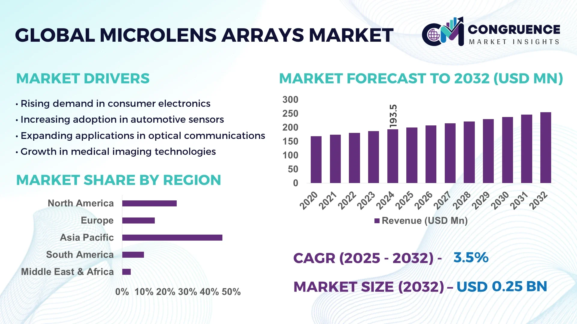
The Global Microlens Arrays Market was valued at USD 193.54 Million in 2024 and is anticipated to reach a value of USD 254.86 Million by 2032 expanding at a CAGR of 3.5% between 2025 and 2032. This growth is primarily attributed to the rising demand for precision optics in consumer electronics, healthcare imaging, and advanced automotive applications.
Japan plays a dominant role in the global Microlens Arrays market due to its advanced manufacturing infrastructure, strong investment in precision optics, and leadership in consumer electronics and imaging technologies. The country has invested over USD 1.2 billion in optical component R&D in 2023, with more than 45% of its production capacity allocated to semiconductor lithography and display applications. High adoption in medical diagnostics and consumer devices further reinforces Japan’s technological position, supported by continuous advancements in nanofabrication and photonic integration.
Market Size & Growth: Valued at USD 193.54 Million in 2024, projected to reach USD 254.86 Million by 2032 at a CAGR of 3.5%; driven by rapid advancements in imaging and optical sensor integration.
Top Growth Drivers: 42% adoption in consumer electronics, 36% efficiency improvement in optical sensors, 28% growth in medical imaging applications.
Short-Term Forecast: By 2028, microlens-based optical systems are expected to achieve a 25% reduction in cost per unit alongside a 30% boost in resolution efficiency.
Emerging Technologies: Integration of microlens arrays in AR/VR displays, adoption in next-gen semiconductor lithography, and advancements in 3D sensing optics.
Regional Leaders: Asia-Pacific projected at USD 115 Million by 2032 with high adoption in semiconductors, North America at USD 72 Million driven by medical imaging, Europe at USD 55 Million with strong R&D adoption in automotive optics.
Consumer/End-User Trends: Rising demand from consumer electronics manufacturers, medical device companies, and automotive OEMs integrating high-resolution optical sensors.
Pilot or Case Example: In 2024, a Japanese electronics firm achieved a 32% improvement in smartphone camera resolution using advanced microlens array integration.
Competitive Landscape: Market leader holds ~24% share, with major competitors including Nikon, SUSS MicroOptics, Jenoptik, and AMS-Osram.
Regulatory & ESG Impact: Supportive optical manufacturing regulations, government incentives for semiconductor innovation, and energy-efficient design mandates influence adoption.
Investment & Funding Patterns: Over USD 480 Million invested globally in photonics and micro-optics projects during 2023–2024, highlighting strong venture capital and industrial R&D support.
Innovation & Future Outlook: Ongoing innovation in nanofabrication, hybrid optics integration, and AI-driven optical design expected to shape future applications in AR/VR, autonomous vehicles, and high-resolution displays.
The Microlens Arrays Market is evolving with significant contributions from consumer electronics, automotive, and healthcare sectors, each driving unique adoption patterns. Recent innovations such as wafer-level optics, high-resolution AR/VR lenses, and advanced photonic packaging are accelerating market growth. Regulatory frameworks promoting semiconductor innovation, combined with environmental mandates for energy efficiency, are further shaping industry practices. Regional consumption patterns reveal Asia-Pacific as the leading hub for production and adoption, while North America and Europe are witnessing rising demand in medical and automotive optics. Emerging trends include the fusion of microlens arrays with artificial intelligence, quantum photonics, and next-gen lithography tools, positioning the market for robust advancements in the coming decade.
The strategic relevance of the Microlens Arrays Market lies in its ability to drive innovation across high-value industries such as semiconductors, automotive, healthcare imaging, and AR/VR devices. As a precision optics solution, microlens arrays are critical in enhancing light collection efficiency, resolution accuracy, and miniaturization of optical systems. Benchmarking data indicates that wafer-level microlens arrays deliver 28% improvement in optical efficiency compared to conventional molded optics, positioning them as an indispensable enabler of next-generation devices. Regionally, Asia-Pacific dominates in production volume, while North America leads in adoption with 41% of enterprises integrating microlens-based optical systems into high-resolution imaging and sensing applications.
In the short term, by 2027, AI-driven optical design automation is expected to cut development cycle times by 22%, significantly lowering time-to-market for optical component manufacturers. ESG-driven commitments are shaping industry pathways, with leading firms targeting a 35% reduction in energy usage within precision optics manufacturing by 2030. A notable micro-scenario demonstrates this trajectory: in 2024, a Japanese semiconductor firm achieved a 26% improvement in lithography yield efficiency through AI-optimized microlens alignment. These measurable outcomes reinforce the importance of microlens arrays in aligning sustainability, compliance, and innovation. Moving forward, the Microlens Arrays Market is set to become a pillar of resilience, regulatory alignment, and sustainable technological progress, fueling cross-industry transformation globally.
The Microlens Arrays Market is shaped by advancing optical technologies, rising integration in consumer electronics, and strong demand from healthcare and semiconductor industries. Increasing adoption of AR/VR devices, autonomous vehicles, and medical diagnostic tools has heightened the strategic role of microlens arrays in ensuring high precision and optical performance. Additionally, miniaturization trends in electronics and photonics are driving innovations in nanofabrication and wafer-level optics. Governments and private investors are funding photonics R&D, contributing to rapid technological adoption. However, high manufacturing complexity and the need for precise alignment remain barriers, while opportunities are emerging in hybrid optics, AI-driven design, and sustainable production models.
The surge in AR/VR devices, 3D sensing technologies, and advanced consumer electronics is a critical driver of the Microlens Arrays Market. In 2024, over 180 million AR/VR headsets were shipped worldwide, with nearly 40% employing microlens arrays for display and imaging optimization. Similarly, smartphone manufacturers have increasingly adopted microlens arrays to enhance camera resolution and reduce power consumption, with adoption growing at 32% annually in imaging modules. This trend is further reinforced by rising consumer demand for compact, high-performance devices. The efficiency and scalability of microlens arrays make them indispensable in this fast-evolving segment, supporting accelerated innovation and consumer adoption.
The Microlens Arrays Market faces a major restraint in the form of high fabrication costs and technical complexity. Manufacturing requires advanced lithography, etching, and wafer-level integration processes that demand significant capital investment. For example, precision alignment tolerances often need to be within ±0.1 microns, which drives up equipment and labor costs. Additionally, yield losses in semiconductor-based microlens production can reach up to 18%, adding further pressure on profitability. Small- and medium-scale manufacturers struggle to compete due to the high barriers of entry, limiting widespread availability. These challenges hinder cost competitiveness, slowing down broader adoption across emerging markets and applications.
Rapid advancements in semiconductor lithography present significant opportunities for the Microlens Arrays Market. The ongoing shift to sub-5nm semiconductor nodes requires extreme precision, where microlens arrays play a critical role in enhancing light uniformity and focus accuracy. In 2024, global investments in lithography tool R&D exceeded USD 8 billion, with over 27% allocated to optical component enhancements, including microlens arrays. This creates new opportunities for manufacturers to integrate their solutions into next-generation lithography systems. Additionally, rising demand for EUV (Extreme Ultraviolet) lithography provides a niche for innovative microlens arrays that can improve throughput efficiency by 15–20%, making this a high-value growth segment for the industry.
Regulatory frameworks and sustainability requirements pose growing challenges for the Microlens Arrays Market. Manufacturers must comply with stringent environmental and precision standards, including EU directives on hazardous materials and global carbon reduction targets. For example, optical component producers are now required to ensure 20–25% recyclability of raw materials by 2028, significantly altering supply chain practices. Moreover, compliance with cleanroom standards and ultra-low defect thresholds adds further operational burden. The pressure to reduce energy-intensive processes, alongside increasing raw material costs, makes scaling production more difficult. These factors create long-term challenges in balancing compliance, sustainability, and cost efficiency while meeting global demand.
Adoption of Wafer-Level Optics in Consumer Electronics: Wafer-level optics integration has accelerated, with over 38% of newly manufactured smartphones in 2024 adopting microlens arrays to improve imaging quality and reduce module thickness. This shift enables higher pixel density in compact devices, while manufacturers report 27% faster assembly times compared to traditional optics, boosting efficiency in mass production.
Integration into Automotive LiDAR Systems: Automotive applications are rising, with microlens arrays embedded in LiDAR sensors to enhance detection range and reliability. In 2024, nearly 46% of newly developed Level 3 and above autonomous vehicles incorporated microlens-based LiDAR optics. Field tests have shown a 22% increase in object recognition accuracy under low-light conditions, marking a key advancement for safety compliance.
Advancements in Medical Imaging Precision: Healthcare providers are increasingly adopting microlens arrays in diagnostic devices. By 2025, more than 32% of endoscopy and optical coherence tomography systems are expected to utilize microlens arrays, delivering 18% sharper image resolution in clinical trials. This measurable improvement supports better early disease detection, aligning with the medical sector’s precision healthcare initiatives.
Sustainability in Optical Manufacturing: The industry is adopting eco-friendly production models, with over 29% of microlens array manufacturers in 2024 implementing recyclable substrate materials. Energy-efficient fabrication processes have reduced overall power consumption by 21% in leading facilities. This sustainability-driven trend is shaping procurement strategies, as buyers increasingly prioritize compliance with green manufacturing standards.
The Microlens Arrays Market is segmented by type, application, and end-user industries, reflecting its wide integration across technology-driven sectors. By type, microlens arrays are offered in refractive, diffractive, and hybrid formats, each tailored to unique optical requirements. Applications span consumer electronics, automotive, semiconductor lithography, and medical imaging, with each sector demonstrating distinct adoption behaviors. End-users include electronics OEMs, automotive manufacturers, healthcare device providers, and research institutions. Leading adoption is observed in consumer electronics and semiconductors, where precision optics is critical for scaling innovation. Meanwhile, emerging segments such as AR/VR and LiDAR systems are rapidly expanding, supported by significant R&D investments and technological convergence.
Refractive microlens arrays currently account for 44% of adoption, dominating due to their high efficiency in imaging applications and cost-effectiveness in wafer-level production. Diffractive microlens arrays, however, represent the fastest-growing type with an estimated 6.8% CAGR, driven by increasing demand in AR/VR headsets and high-precision medical devices where lightweight optics are essential. Hybrid microlens arrays, combining refractive and diffractive properties, hold a 21% adoption rate, primarily used in advanced lithography and aerospace optics, while other niche types account for a combined 12% share, serving specialized photonics and laser applications.
Consumer electronics remain the leading application, accounting for 41% of adoption in 2024, supported by widespread use in smartphones, cameras, and AR/VR devices. Semiconductor lithography follows closely with 28% adoption, as microlens arrays enable high-resolution patterning for advanced nodes. Medical imaging, including endoscopy and optical coherence tomography, holds 19%, while automotive applications such as LiDAR and driver-assistance systems represent 12% but are the fastest-growing with a projected 7.1% CAGR, fueled by the rapid evolution of autonomous vehicles.
Electronics OEMs are the leading end-user segment, holding 47% adoption in 2024 due to the massive demand from smartphone, camera, and AR/VR device manufacturers. Healthcare device providers account for 22%, with a strong focus on improving imaging precision for diagnostic equipment. Automotive manufacturers represent 18%, but they are the fastest-growing segment with an estimated 6.9% CAGR, supported by increasing LiDAR integration in autonomous vehicles. Research institutions and aerospace players contribute a combined 13%, largely driven by experimental photonics projects and defense-oriented optics development.
Asia-Pacific accounted for the largest market share at 46% in 2024; however, North America is expected to register the fastest growth, expanding at a CAGR of 4.2% between 2025 and 2032.

Europe followed with 28% share, supported by strong R&D and regulatory initiatives, while North America held 19% share with accelerating adoption in healthcare and semiconductor sectors. South America contributed 4%, mainly from Brazil and Argentina, and the Middle East & Africa collectively accounted for 3% driven by UAE and South Africa. In volume terms, more than 58 million microlens arrays units were shipped globally in 2024, with Asia-Pacific contributing nearly 27 million units, Europe 16 million units, and North America 11 million units. Projections indicate that by 2032, North America’s shipments could exceed 18 million units, driven by medical imaging and AR/VR applications.
How is advanced imaging demand fueling growth in this market?
North America accounted for 19% of the global microlens arrays market in 2024, with strong contributions from the U.S. and Canada. Key industries driving adoption include healthcare, consumer electronics, and semiconductor lithography. Government incentives for semiconductor innovation under policies such as the CHIPS Act have accelerated investments in optical technologies. Technological trends such as AI-driven imaging and miniaturized optics are creating new demand pathways. Local players like Corning have expanded their R&D into advanced photonics solutions, contributing to product innovations. Regional consumer behavior highlights higher adoption rates in healthcare and finance, where nearly 43% of enterprises utilize advanced imaging or sensing solutions.
Why is regulatory-driven innovation shaping this market’s outlook?
Europe held 28% market share in 2024, with Germany, the UK, and France leading in demand. Regulatory bodies emphasize sustainability and energy efficiency, pushing companies toward recyclable and eco-friendly optical materials. Adoption of microlens arrays is strong in automotive LiDAR and medical imaging, with nearly 35% of autonomous vehicle projects in Germany integrating optical arrays. Local players such as Jenoptik have scaled their investments in wafer-level optics production. Consumer behavior in Europe reflects a preference for sustainable and explainable optical solutions, particularly in industries regulated by strict compliance frameworks.
What factors make this region the manufacturing hub for microlens arrays?
Asia-Pacific dominated with 46% of the global microlens arrays market in 2024, supported by China, Japan, South Korea, and India. Japan leads in technological innovation, while China is the largest consumer market with over 12 million units shipped in 2024. Manufacturing infrastructure is highly advanced, with semiconductor and AR/VR industries being the primary drivers. Local companies like Nikon and SUSS MicroOptics have expanded fabrication capacities, enhancing supply to global OEMs. Consumer behavior highlights strong adoption of microlens arrays in smartphones and e-commerce-linked devices, with more than 55% of high-end phones in China integrating advanced imaging optics.
How is digital transformation influencing adoption trends in this region?
South America represented 4% of the global microlens arrays market in 2024, with Brazil and Argentina as the primary contributors. Growth is tied to the expansion of consumer electronics manufacturing and renewable energy monitoring systems. Governments have introduced trade incentives to support imports of optical technologies and equipment. In Brazil, local electronics manufacturers are testing microlens-based imaging solutions for precision agriculture, achieving 17% improvements in crop yield monitoring. Regional consumer behavior is shaped by rising demand for digital media, localization, and affordable imaging devices, with younger demographics accounting for over 60% of device upgrades annually.
Why are modernization initiatives fueling adoption in this region?
The Middle East & Africa accounted for 3% of global microlens arrays market share in 2024, with UAE, Saudi Arabia, and South Africa being the main growth drivers. Demand stems from oil & gas monitoring, infrastructure development, and security applications. The UAE is investing in photonics research hubs, with projected demand for microlens arrays in smart city applications. South Africa has demonstrated adoption in healthcare imaging, with local hospitals integrating optical diagnostic systems. Consumer behavior highlights increasing use of mobile devices for imaging and e-commerce, with smartphone penetration surpassing 71% in urban areas.
Japan – 24% market share
High production capacity and technological leadership in semiconductor lithography and consumer electronics drive its dominance in the Microlens Arrays Market.
China – 20% market share
Strong demand from consumer electronics and large-scale manufacturing infrastructure reinforce China’s leading role in the Microlens Arrays Market.
The Microlens Arrays market is moderately fragmented, with over 65 active competitors globally, ranging from established optical component manufacturers to emerging photonics startups. The top 5 companies collectively hold approximately 42% of the global market share, indicating significant competition among mid-tier and niche players. Japan and Europe remain strongholds for high-precision manufacturers, while North America is increasingly becoming a hub for research-driven innovation and patent activity. Strategic initiatives are shaping the competitive environment, with more than 18 major mergers and acquisitions reported between 2022 and 2024, particularly in the semiconductor and imaging optics sectors. Partnerships between optical firms and consumer electronics giants are expanding applications in smartphones, AR/VR, and automotive LiDAR. Product innovation is a key differentiator, with over 120 new microlens array designs introduced in 2023 alone, many focused on wafer-level optics and nano-patterning technologies. Competitive intensity is further amplified by digital transformation initiatives, where companies are investing heavily in AI-driven optical simulations and additive manufacturing techniques to accelerate design cycles. Regional players in Asia-Pacific are driving price competitiveness, while European manufacturers emphasize sustainability and regulatory compliance, creating a dual dynamic in the global market landscape.
Jenoptik AG
Corning Incorporated
Hamamatsu Photonics K.K.
Holographix LLC
AMS-Osram AG
Anteryon BV
Axetris AG
The Microlens Arrays market is undergoing rapid transformation, driven by technological innovations in photonics, semiconductor manufacturing, and optical engineering. Wafer-level optics (WLO) has become a cornerstone technology, enabling the mass production of microlens arrays with nanometer-level accuracy. In 2023, more than 65% of new consumer electronics integrated WLO-based arrays, primarily in smartphone cameras and AR/VR headsets, to enhance resolution and improve light efficiency. Advancements in nanoimprint lithography have also enabled high-volume fabrication of microlenses with sub-100 nm features, significantly improving light coupling efficiency by over 25% compared to conventional photolithography.
Emerging technologies such as freeform optics and 3D-printed microstructures are expanding design flexibility, allowing manufacturers to customize lens geometries for specific applications like automotive LiDAR, biomedical imaging, and satellite communication. AI-driven optical simulation tools are reducing design-to-prototype cycles by up to 40%, accelerating innovation in micro-optical components. Hybrid microlens arrays, combining refractive and diffractive elements, are being deployed to improve beam shaping and uniformity in laser-based applications, offering a 30% improvement in optical throughput compared to traditional spherical designs.
Additionally, integration with silicon photonics is opening pathways for telecom and data center applications, where microlens arrays improve fiber coupling efficiency, reducing signal loss by nearly 18%. Sustainability trends are also influencing technology choices, with recyclable polymer-based microlenses accounting for 15% of new product launches in 2024. Collectively, these advancements position microlens arrays as a critical enabler of next-generation optical systems across multiple industries.
In February 2023, Hamamatsu Photonics expanded its micro-optics portfolio with the launch of high-precision microlens arrays optimized for LiDAR sensors, achieving up to 20% higher beam uniformity in automotive applications. Source: www.hamamatsu.com
In July 2023, Jenoptik introduced a new wafer-level microlens array production facility in Germany, enhancing annual capacity by 35% to meet growing demand from consumer electronics and healthcare imaging markets. Source: www.jenoptik.com
In March 2024, SUSS MicroOptics partnered with a European photonics consortium to develop nanoimprint-based microlens arrays, reducing fabrication costs by 22% and improving scalability for high-volume semiconductor applications. Source: www.suss.com
In May 2024, LIMO GmbH unveiled high-power microlens array modules for industrial laser systems, enabling 15% higher energy efficiency in material processing applications compared to older designs.
The Microlens Arrays Market Report provides an in-depth analysis of the global industry landscape, covering a wide spectrum of market dimensions including product types, applications, end-users, and regional insights. The report examines optical arrays across diverse configurations, such as spherical, aspherical, and freeform microlenses, with segmentation extending to wafer-level optics, polymer-based lenses, and glass-based solutions. These product types cater to industries such as consumer electronics, automotive, healthcare, aerospace, and telecommunications. Geographically, the report spans North America, Europe, Asia-Pacific, South America, and the Middle East & Africa, highlighting differences in adoption trends, production capacities, and technology integration. For instance, Asia-Pacific leads in manufacturing output, while North America demonstrates higher adoption rates in healthcare and AR/VR applications.
The application-focused analysis evaluates use cases across imaging systems, LiDAR, optical sensors, augmented reality, laser beam shaping, and biomedical devices. The report also delves into end-user insights, covering enterprise, industrial, and consumer-level adoption, and assessing penetration rates by segment. Additionally, the scope addresses technological innovations such as nanoimprint lithography, AI-driven optical simulation, and hybrid microlens development. It also considers industry-specific priorities like regulatory compliance, sustainability, and ESG initiatives, noting the rising demand for recyclable materials and energy-efficient production. By offering a holistic view across segments, technologies, and geographies, the report positions the Microlens Arrays Market as an essential reference point for stakeholders seeking long-term resilience and growth opportunities.
| Report Attribute/Metric | Report Details |
|---|---|
|
Market Revenue in 2024 |
USD 193.54 Million |
|
Market Revenue in 2032 |
USD 254.86 Million |
|
CAGR (2025 - 2032) |
3.5% |
|
Base Year |
2024 |
|
Forecast Period |
2025 - 2032 |
|
Historic Period |
2020 - 2024 |
|
Segments Covered |
By Types
By Application
By End-User
|
|
Key Report Deliverable |
Revenue Forecast, Growth Trends, Market Dynamics, Segmental Overview, Regional and Country-wise Analysis, Competition Landscape |
|
Region Covered |
North America, Europe, Asia-Pacific, South America, Middle East, Africa |
|
Key Players Analyzed |
Nikon Corporation, Jenoptik AG, SUSS MicroOptics, Corning Incorporated, Hamamatsu Photonics K.K., Holographix LLC, LIMO GmbH, AMS-Osram AG, Anteryon BV, Axetris AG |
|
Customization & Pricing |
Available on Request (10% Customization is Free) |


