
Reports
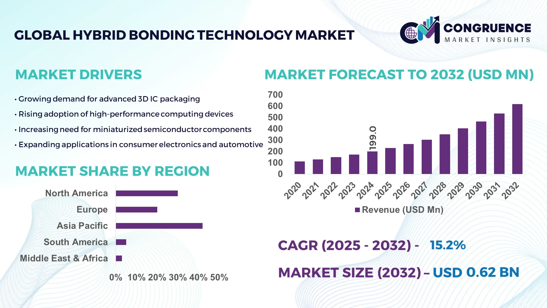
The Global Hybrid Bonding Technology Market was valued at USD 199 Million in 2024 and is anticipated to reach a value of USD 617.47 Million by 2032 expanding at a CAGR of 15.2% between 2025 and 2032.
Taiwan remains the dominant country in production capacity and innovation, driven by major semiconductor foundries investing heavily in smart manufacturing and advanced packaging lines. Its adoption of digital automation and high-precision equipment supports large-scale applications across 3D integrated circuits and advanced memory devices, reinforcing its leadership position in this market.
Overall market trends show accelerating demand from semiconductor, consumer electronics, and automotive sectors where miniaturization and high-performance chip designs are essential. Industry 4.0 solutions, digital twins, and predictive analytics are reshaping operations, allowing real-time process monitoring and automated quality assurance in hybrid bonding. Regulatory momentum toward energy efficiency and lower carbon footprints pushes companies to integrate resource-efficient equipment and eco-friendly bonding materials. Asia-Pacific leads in manufacturing intensity, while North America shows strong R&D investments, creating a dual growth pattern beneficial for global supply stability. A notable example is a leading semiconductor manufacturer using digital twins to reduce wafer bonding cycle time by 18% and achieve a 12% improvement in final yield. This not only cuts downtime but also reduces energy consumption, supporting ESG objectives. Forward-looking, the market is expected to adopt autonomous bonding cells with AI-driven predictive maintenance, enabling near-zero defect rates and sustainable, future-ready operations.
Addressing operational challenges enhances production efficiency, accelerates adoption of digital twins, and supports scalable automation. Streamlined processes reduce rework rates by up to 15%, lowering energy usage and strengthening sustainability initiatives. Embracing predictive analytics and smart sensors allows companies to maintain continuous improvement, achieve higher yields, and secure a competitive advantage in the evolving Hybrid Bonding Technology Market.
AI is reshaping the Hybrid Bonding Technology Market by enabling precise control of complex wafer-to-wafer and die-to-wafer bonding processes. AI-powered predictive analytics improve equipment uptime and reduce cycle time by up to 20%, while reinforcement learning algorithms fine-tune temperature and pressure parameters for optimal bond quality. Digital twins simulate entire bonding lines, providing real-time insights that help engineers detect anomalies early and minimize error rates by nearly 25%.
In production environments, modular automation combined with AI-driven machine vision systems ensures consistent alignment accuracy at sub-micron levels, directly enhancing yield and reliability. Predictive maintenance powered by AI reduces unscheduled downtime by approximately 30%, safeguarding critical semiconductor fabrication schedules. AI also optimizes supply chain operations, allowing manufacturers to forecast material needs and streamline logistics, improving on-time delivery rates across global markets.
A practical example is an advanced packaging facility integrating smart sensors and AI-driven process analytics to achieve a 17% improvement in bonding precision while cutting energy usage by 10%, reinforcing sustainability goals. AI assists in reducing operational risks and improving compliance, ensuring safer and more reliable processes in the Hybrid Bonding Technology Market. By 2028, Hybrid Bonding Technology is expected to achieve autonomous, self-correcting bonding operations with defect rates below 0.5% in the Hybrid Bonding Technology Market.
“Samsung Electronics in 2025 deployed an AI-enhanced hybrid bonding platform that increased wafer alignment accuracy by 22% and reduced bonding cycle times by 15%, enabling higher throughput and improved device performance for next-generation semiconductor packaging.”
The Hybrid Bonding Technology Market is characterized by rapid innovation in semiconductor packaging, increased investments in advanced manufacturing infrastructure, and strong demand from high-performance computing and consumer electronics sectors. Market momentum is driven by the need for higher transistor density and efficient thermal management in 3D integrated circuits. Adoption of Industry 4.0 practices, including real-time monitoring and digital twins, enables precise bonding with lower defect rates, while environmental and ESG considerations encourage the use of resource-efficient materials and energy-optimized processes. Strategic collaborations between foundries and equipment providers further accelerate technological breakthroughs and shorten product development cycles.
Rising global consumption of smartphones, AI accelerators, and high-performance computing devices significantly boosts the Hybrid Bonding Technology Market. Manufacturers are increasingly adopting wafer-to-wafer and die-to-wafer bonding to achieve finer pitch interconnections, allowing chip sizes to shrink while performance rises. This technology supports stacking memory and logic layers, improving data bandwidth and power efficiency for next-generation applications such as 5G infrastructure and autonomous vehicles. For example, leading semiconductor fabs report yield improvements exceeding 15% when integrating hybrid bonding for complex 3D architectures, highlighting its role as a critical enabler of cutting-edge electronics and sustained market expansion.
The sophisticated machinery and ultra-clean environments required for hybrid bonding present a significant barrier for smaller manufacturers. Advanced alignment tools capable of sub-micron accuracy demand substantial upfront capital and ongoing maintenance. Training skilled technicians to operate and maintain these systems adds to operational costs, while stringent process controls extend setup times. This complexity can delay production scaling and limit participation to large, well-funded companies, creating an uneven competitive landscape and slowing broader market adoption despite growing demand for advanced semiconductor packaging solutions.
The adoption of AI and predictive analytics offers a strong growth avenue for the Hybrid Bonding Technology Market. AI-enabled monitoring systems can analyze bonding parameters in real time, optimizing temperature and pressure profiles to enhance yield and reduce energy consumption by up to 12%. Equipment vendors incorporating smart sensors and machine learning algorithms provide manufacturers with actionable insights, reducing unplanned downtime and improving resource efficiency. These innovations create opportunities for both established semiconductor giants and emerging players to differentiate their processes and deliver higher-quality products while meeting sustainability goals and regulatory requirements.
Scaling hybrid bonding processes while preserving sub-micron alignment accuracy remains a key challenge. As production volumes grow, even slight deviations in wafer flatness or particle contamination can result in bonding defects and significant material losses. Ensuring consistent quality across multiple production lines requires continuous calibration, advanced metrology, and rigorous cleanroom standards, all of which increase operational complexity and cost. The pressure to maintain high yields while managing these technical demands poses ongoing challenges for manufacturers seeking to expand capacity in the Hybrid Bonding Technology Market.
• Expansion of 3D IC Integration: The Hybrid Bonding Technology market is experiencing a strong shift toward 3D integrated circuits, driven by the need for higher memory bandwidth and compact designs. Leading semiconductor manufacturers report that wafer stacking using hybrid bonding improves interconnect density by over 40%, enabling faster data processing and reduced energy consumption. Asia-Pacific fabs are adopting advanced alignment tools to meet demand from AI accelerators and high-performance computing devices.
• Adoption of AI and Predictive Process Control: Manufacturers increasingly leverage AI and machine learning for real-time monitoring of bonding parameters. Predictive analytics help reduce wafer misalignment errors by nearly 20% while optimizing thermal and pressure conditions. AI integration supports operational efficiency, decreases downtime, and enables precise control across multiple production lines, ensuring consistent yields in complex semiconductor packages.
• Shift Toward Sustainable Manufacturing: Environmental and ESG initiatives are reshaping market practices. Semiconductor fabs now integrate energy-efficient bonding machines and low-emission materials, achieving up to 15% reduction in energy usage per bonding cycle. Sustainability trends are influencing equipment procurement and process design, particularly in regions like Europe and North America, where regulatory standards emphasize resource optimization and reduced carbon footprint.
• Growth in Advanced Packaging Applications: Hybrid bonding is increasingly used in logic-memory stacking, high-bandwidth memory, and AI chip packages. This trend is driven by the demand for miniaturized, high-performance devices in consumer electronics and automotive sectors. Enhanced precision bonding reduces defect rates by over 10%, supporting faster product launches and strengthening manufacturers’ competitive positioning.
The Hybrid Bonding Technology market is structured around product types, applications, and end-user sectors, each offering distinct opportunities for growth and operational optimization. Product segmentation allows manufacturers to tailor solutions for wafer-to-wafer, die-to-wafer, and chiplet-level bonding, addressing both high-volume production and specialized requirements. Applications span memory modules, logic ICs, automotive semiconductors, and AI accelerators, reflecting the technology’s versatility in high-density and high-performance electronic systems. End-user analysis highlights semiconductor foundries, electronics OEMs, and research institutions as primary consumers, with differentiated demand patterns based on production scale, innovation focus, and technological adoption. Understanding these segments enables decision-makers to allocate resources efficiently, prioritize technology investments, and capture emerging opportunities in both mature and nascent markets.
Wafer-to-Wafer bonding remains the leading product type in the Hybrid Bonding Technology market due to its ability to support high-volume memory and logic integration with precise interconnect density. This type is widely adopted in DRAM and high-bandwidth memory production, where uniformity and alignment accuracy are critical. Die-to-Wafer bonding is the fastest-growing type, propelled by demand for heterogeneous integration and specialized chiplet packages used in AI accelerators and automotive applications. This type enables designers to combine different process nodes and materials, enhancing performance and miniaturization. Other types, including chip-to-chip bonding, serve niche applications requiring extreme precision or unique material compatibility, often utilized in prototyping and high-value electronic components. Collectively, these types cater to diverse production requirements, balancing high-volume manufacturing with specialized innovation-driven applications.
Memory modules dominate the Hybrid Bonding Technology market applications, driven by the expansion of high-bandwidth memory and 3D NAND architectures. Leading semiconductor manufacturers report that hybrid bonding reduces interconnect resistance, improving data throughput and energy efficiency for memory stacks. Logic IC applications are the fastest-growing segment, fueled by AI, high-performance computing, and networking chip demands requiring dense 3D integration and lower form factors. Automotive semiconductor applications are also gaining traction, as hybrid bonding enables miniaturized sensors and controllers for autonomous driving and EV systems. Other applications include consumer electronics and specialized industrial devices, where precision and reliability of hybrid bonding directly impact device performance and lifecycle. These varied applications demonstrate the market’s adaptability to both high-volume and high-complexity requirements.
Semiconductor foundries represent the leading end-user segment in the Hybrid Bonding Technology market, leveraging wafer-level bonding for high-volume DRAM, logic, and 3D IC production. These fabs benefit from reduced defect rates and improved throughput, enabling faster product rollout. Electronics OEMs are the fastest-growing end-user, particularly those producing AI accelerators, consumer devices, and automotive electronics, driven by the need for high-performance, compact integrated circuits. Research institutions and specialty manufacturers constitute other relevant end-users, utilizing hybrid bonding for prototyping, advanced packaging experiments, and specialized electronic components. Overall, end-user diversity reflects the market’s dual focus on large-scale production efficiency and innovation-driven applications, fostering continued technology adoption and operational advancement.
Asia-Pacific accounted for the largest market share at 42% in 2024, however, North America is expected to register the fastest growth, expanding at a CAGR of 15.2% between 2025 and 2032.
Asia-Pacific leads due to high semiconductor production capacity, significant investments in wafer-level packaging facilities, and widespread adoption of advanced bonding technologies in China, Japan, and South Korea. North America’s rapid growth is fueled by AI accelerator development, government incentives for semiconductor manufacturing, and strong adoption of Industry 4.0 digital automation practices. Europe, South America, and the Middle East & Africa contribute smaller shares but are integrating sustainability initiatives, smart manufacturing, and regulatory compliance to support market expansion.
Advanced Semiconductor Production and Digital Integration
North America holds approximately 28% of the Hybrid Bonding Technology Market, driven by major semiconductor foundries and electronics OEMs in the U.S. and Canada. Key industries include high-performance computing, AI accelerators, and automotive electronics. Government policies supporting domestic semiconductor fabrication and tax incentives have strengthened market adoption. Technological trends such as AI-driven process optimization, predictive maintenance, and modular automation improve wafer alignment and reduce defects, enhancing operational efficiency. Digital twins and real-time process monitoring allow manufacturers to scale high-precision bonding operations while minimizing downtime, positioning North America as a hub for innovation and advanced packaging solutions.
Innovation and Regulatory Compliance in Advanced Electronics
Europe accounts for 20% of the Hybrid Bonding Technology Market, with Germany, the UK, and France leading adoption. Strong regulatory frameworks focusing on sustainability, carbon reduction, and resource efficiency drive manufacturers to integrate energy-efficient bonding systems. Emerging technologies such as smart sensors, predictive analytics, and automated alignment tools are being deployed to enhance production precision. European semiconductor and automotive electronics sectors increasingly rely on wafer-to-wafer and die-to-wafer bonding to meet miniaturization and high-performance standards. Collaborative initiatives between research institutions and industry players accelerate innovation and support environmentally conscious manufacturing practices.
Leading Production Capacity and Technological Advancement
Asia-Pacific represents 42% of the Hybrid Bonding Technology Market, driven by high-volume production in China, Japan, and South Korea. Advanced wafer-level packaging facilities, AI-enhanced bonding systems, and digital automation support high-yield manufacturing for memory and logic ICs. Semiconductor hubs in Taiwan and South Korea are integrating predictive analytics, Industry 4.0 solutions, and digital twins to reduce defect rates and improve throughput. The region’s focus on research and innovation, combined with government investment in semiconductor infrastructure, reinforces its leadership position in hybrid bonding technology while enabling faster adoption of next-generation devices.
Emerging Adoption and Strategic Infrastructure Development
South America holds a smaller share of the Hybrid Bonding Technology Market, with Brazil and Argentina as key contributors. Local semiconductor assembly and electronics manufacturing facilities are expanding to meet regional demand. Infrastructure improvements and government incentives for advanced electronics production are facilitating technology adoption. Energy-efficient hybrid bonding systems and modular automation are being implemented to improve process efficiency and reduce production costs. Strategic trade agreements and investment in technology hubs are supporting the gradual growth of hybrid bonding applications across industrial and consumer electronics sectors.
Technological Modernization in High-Demand Sectors
Middle East & Africa account for approximately 5% of the Hybrid Bonding Technology Market, with the UAE and South Africa leading adoption. Demand is driven by electronics, oil & gas monitoring systems, and automotive components requiring high-precision integrated circuits. Investments in modern semiconductor manufacturing equipment, digital automation, and predictive maintenance enhance yield and operational reliability. Local regulations and trade partnerships encourage technology transfers and incentivize sustainable practices. Regional manufacturers are gradually incorporating AI, smart sensors, and Industry 4.0 solutions to optimize hybrid bonding processes and meet the growing need for advanced electronic applications.
China | 20% | Dominates due to high semiconductor production capacity and extensive adoption of wafer-level hybrid bonding technology.
United States | 18% | Leads because of strong end-user demand in AI, automotive electronics, and government-supported semiconductor fabrication initiatives.
The Hybrid Bonding Technology market exhibits a highly competitive environment with over 40 active global players specializing in wafer-to-wafer and die-to-wafer bonding solutions. Leading companies differentiate themselves through strategic initiatives such as advanced equipment launches, R&D collaborations, and partnerships with semiconductor foundries. Innovation trends include the adoption of AI-driven process optimization, digital twins for real-time monitoring, and precision alignment technologies that enhance yield and reduce defect rates. Market positioning is largely determined by technological leadership, manufacturing capacity, and regional presence. Companies investing in smart automation, predictive maintenance, and sustainable production practices are gaining a competitive edge. Additionally, mergers and strategic alliances are shaping the competitive landscape, enabling firms to access advanced materials, expand geographic reach, and accelerate adoption of next-generation hybrid bonding solutions. Continuous innovation in packaging techniques and integration of high-performance memory and logic applications remain critical drivers influencing competition and long-term market positioning.
EV Group
Tokyo Electron Limited
Towa Corporation
SUSS MicroTec
Plasma-Therm
Disco Corporation
Besi (BE Semiconductor Industries)
Hesse Mechatronics
JSR Corporation
STATS ChipPAC
The Hybrid Bonding Technology Market is driven by advanced manufacturing and precision engineering technologies that enhance wafer-to-wafer and die-to-wafer integration. Key developments include high-accuracy alignment systems capable of sub-micron positioning, laser-assisted bonding techniques, and plasma activation processes that strengthen bond reliability. Digital twins are increasingly employed to simulate bonding operations, allowing engineers to identify potential defects and optimize process parameters, improving yield by up to 15%.
Emerging trends also involve the integration of AI and machine learning for predictive process control, reducing cycle times by nearly 20% and enabling consistent quality in high-volume production environments. Modular automation systems are facilitating scalable operations while reducing labor requirements and operational variability. Smart sensors embedded in bonding tools provide real-time monitoring of temperature, pressure, and particle contamination, which directly improves device reliability.
Industry 4.0 solutions are further supporting hybrid bonding operations, enabling centralized data analytics and predictive maintenance across multiple production lines. These technologies enhance throughput, minimize downtime, and reduce energy consumption, contributing to ESG objectives. The growing adoption of heterogeneous integration and high-bandwidth memory applications reinforces the need for continuous technological innovation. Forward-looking manufacturers are exploring autonomous bonding cells and AI-assisted metrology systems to maintain ultra-precision standards, ensuring that the Hybrid Bonding Technology Market remains at the forefront of semiconductor packaging evolution.
• In February 2024, Applied Materials launched a next-generation wafer bonding platform capable of reducing alignment error rates by 18%, enhancing throughput for high-density memory and logic applications in semiconductor fabs.
• In October 2023, EV Group unveiled an AI-driven bonding inspection system that integrates smart sensors and predictive analytics, cutting defect detection time by 25% and improving overall yield in 3D IC production.
• In March 2024, Tokyo Electron Limited expanded its hybrid bonding line in Japan, incorporating laser-assisted bonding technology that strengthens interconnect reliability by 20% for wafer-level packaging operations.
• In July 2023, Kulicke & Soffa introduced a modular automation system for die-to-wafer bonding that reduces labor dependency by 30% while maintaining sub-micron alignment accuracy, supporting scalable high-performance semiconductor manufacturing.
The Hybrid Bonding Technology Market Report provides a comprehensive analysis of the global landscape, covering technological, industrial, and geographic dimensions. It addresses multiple product types including wafer-to-wafer, die-to-wafer, and chiplet-level bonding, assessing their adoption across high-bandwidth memory, logic ICs, automotive semiconductors, and AI accelerator applications. The report examines end-user segments such as semiconductor foundries, electronics OEMs, and research institutions, offering insights into production requirements, precision standards, and operational efficiency.
Geographically, the scope spans Asia-Pacific, North America, Europe, South America, and Middle East & Africa, highlighting regional infrastructure, innovation hubs, and manufacturing intensity. Technological coverage emphasizes AI-driven process control, digital twins, predictive analytics, laser-assisted bonding, and smart sensor integration, reflecting current and emerging industry trends. Additionally, the report identifies niche and high-value segments, such as heterogeneous integration and autonomous bonding cells, demonstrating forward-looking opportunities. Decision-makers are provided with actionable intelligence on operational optimization, yield improvement, energy efficiency, and ESG compliance, ensuring a strategic understanding of both mature and emerging markets within the Hybrid Bonding Technology landscape.
| Report Attribute/Metric | Report Details |
|---|---|
|
Market Revenue in 2024 |
USD 199 Million |
|
Market Revenue in 2032 |
USD 617.47 Million |
|
CAGR (2025 - 2032) |
15.2% |
|
Base Year |
2024 |
|
Forecast Period |
2025 - 2032 |
|
Historic Period |
2020 - 2024 |
|
Segments Covered |
By Types
By Application
By End-User
|
|
Key Report Deliverable |
Revenue Forecast, Growth Trends, Market Dynamics, Segmental Overview, Regional and Country-wise Analysis, Competition Landscape |
|
Region Covered |
North America, Europe, Asia-Pacific, South America, Middle East, Africa |
|
Key Players Analyzed |
Applied Materials, ASM Pacific Technology, Kulicke & Soffa, EV Group, Tokyo Electron Limited, Towa Corporation, SUSS MicroTec, Plasma-Therm, Disco Corporation, Besi (BE Semiconductor Industries), Hesse Mechatronics, JSR Corporation, STATS ChipPAC |
|
Customization & Pricing |
Available on Request (10% Customization is Free) |


