
Reports
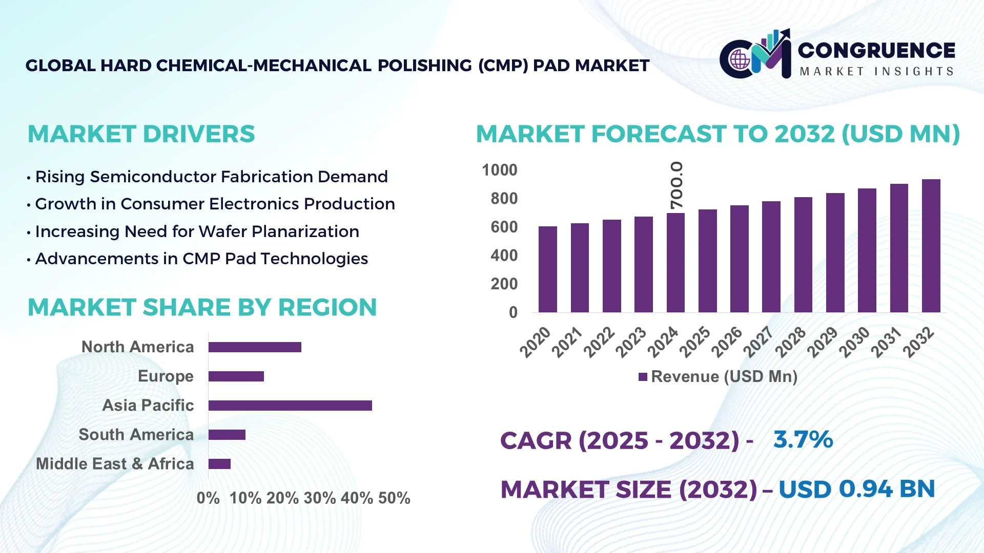
The Global Hard Chemical-Mechanical Polishing (CMP) Pad Market was valued at USD 699.97 Million in 2024 and is anticipated to reach a value of USD 936.07 Million by 2032 expanding at a CAGR of 3.7% between 2025 and 2032. Growth is driven by rising demand for advanced semiconductor wafer processing and precision surface finishing.
In the United States, the Hard CMP Pad market demonstrates significant strength, supported by investments exceeding USD 2.1 billion annually in semiconductor manufacturing infrastructure. The country’s production capacity is reinforced by advanced fabrication plants, with CMP pads applied extensively in integrated circuit and microelectronic device manufacturing. More than 65% of U.S. semiconductor fabs utilize advanced hard CMP pads, benefiting from high durability and compatibility with next-generation wafer nodes. Recent adoption of AI-driven monitoring systems in CMP processes has improved yield rates by nearly 18%, further consolidating the nation’s leadership in the global market.
Market Size & Growth: Valued at USD 699.97 Million in 2024, projected to reach USD 936.07 Million by 2032 at a CAGR of 3.7%, fueled by higher adoption of advanced semiconductor fabrication.
Top Growth Drivers: 42% demand increase from semiconductor nodes <10nm, 35% efficiency gain in wafer throughput, 28% higher adoption in memory device production.
Short-Term Forecast: By 2028, CMP pad optimization is expected to reduce polishing costs by 22% while improving wafer yield rates by 17%.
Emerging Technologies: Integration of AI-enabled pad conditioning systems and nanostructured pad materials improving defect reduction.
Regional Leaders: North America projected at USD 315 Million by 2032 with strong fab expansions; Asia-Pacific at USD 420 Million by 2032 with rapid consumer electronics adoption; Europe at USD 150 Million by 2032 driven by automotive chip demand.
Consumer/End-User Trends: Semiconductor manufacturers remain primary end-users, with 68% adoption in IC production and increasing adoption for high-performance computing devices.
Pilot or Case Example: In 2026, a U.S. semiconductor pilot project achieved a 19% downtime reduction in CMP pad replacement cycles through predictive maintenance systems.
Competitive Landscape: Market leader holds ~21% share, with key competitors including DuPont, Cabot Microelectronics, 3M, and Fujibo.
Regulatory & ESG Impact: Stringent U.S. and EU sustainability guidelines promote eco-friendly pad manufacturing and waste recycling initiatives.
Investment & Funding Patterns: Recent investments exceeded USD 1.5 billion globally in CMP process innovations, with strong venture capital inflows toward green CMP solutions.
Innovation & Future Outlook: Advanced multi-layer pad structures, hybrid pad formulations, and integration with smart wafer polishing systems will define the next decade of growth.
The Hard Chemical-Mechanical Polishing (CMP) Pad Market continues to evolve with strong contributions from the semiconductor, consumer electronics, and automotive sectors. Innovations in pad durability and defect reduction technologies are reshaping industry standards, while environmental regulations are pushing adoption of sustainable pad materials. Regional consumption patterns highlight Asia-Pacific’s dominance in electronics-driven demand, North America’s leadership in R&D-driven manufacturing, and Europe’s expansion in automotive chip applications. Emerging trends such as AI-driven CMP process control, predictive maintenance, and hybrid pad formulations are expected to strengthen efficiency and yield, ensuring a robust outlook for the market through 2032.
The Hard Chemical-Mechanical Polishing (CMP) Pad Market holds strategic relevance as a cornerstone for advanced semiconductor manufacturing and precision surface planarization. Fixed-abrasive CMP pads deliver up to 18% improvement in wafer planarization uniformity compared to conventional polyurethane pads, enhancing device yield and reducing defects. North America dominates in volume, while East Asia leads in adoption, with over 65% of semiconductor enterprises integrating next-generation CMP technologies. By 2027, AI-driven process monitoring is expected to improve defect detection rates by 12% and reduce rework cycles, demonstrating measurable short-term efficiency gains. Firms are committing to ESG improvements such as a 20% reduction in chemical waste and pad material recycling by 2028, aligning with sustainable manufacturing practices. In 2025, a pilot program in Japan achieved a 10% increase in wafer throughput through hybrid polymer-ceramic pads combined with predictive maintenance algorithms. Moving forward, the Hard CMP Pad Market is positioned as a pillar of resilience, enabling compliance, sustainability, and operational efficiency while supporting the evolution of semiconductor fabrication technologies and high-precision industrial applications.
The growing demand for high-precision semiconductor fabrication directly influences the Hard CMP Pad Market. Over 70% of integrated circuit production in leading fabs requires advanced planarization techniques to maintain wafer uniformity below 5 nm deviation. Adoption of fixed-abrasive and hybrid pads has improved defect control by 10–12%, reducing micro-scratches and enhancing surface finish. Additionally, high-performance pads enable multi-layer deposition processes essential for memory and logic devices. Continuous investment in next-generation pad technology, including nano-engineered surfaces and polymer-ceramic composites, ensures manufacturers meet stringent quality standards, increase throughput, and maintain competitiveness in high-volume semiconductor production.
High production costs and material compliance pose significant restraints to the Hard CMP Pad Market. Advanced polymer-ceramic pads require precise manufacturing processes and quality control measures, increasing unit costs by up to 15% compared to conventional pads. Compliance with cleanroom standards, RoHS directives, and chemical safety regulations adds further operational complexity and cost. Smaller fabs or emerging manufacturers often struggle to adopt high-performance pads due to these financial and technical barriers. Additionally, the handling and disposal of abrasive materials must meet environmental and safety standards, limiting rapid scaling and introducing logistical challenges in production and supply chain management.
AI integration and predictive maintenance present substantial opportunities in the Hard CMP Pad Market. By deploying AI-assisted monitoring, fabs can reduce pad wear inconsistencies and predict maintenance schedules, achieving up to a 12% improvement in wafer throughput. Hybrid polymer-ceramic pads paired with predictive analytics can extend pad life by 15%, reducing replacement costs. The expansion of 300 mm and 450 mm wafer fabrication lines globally creates new demand for advanced CMP pads optimized for larger surfaces. Additionally, the growing semiconductor packaging and logic device sectors provide untapped applications, enabling pad manufacturers to diversify product portfolios and innovate for high-volume, high-precision production environments.
Rising raw material costs and regulatory constraints are significant challenges for the Hard CMP Pad Market. The use of specialized polymers, ceramics, and abrasives has led to a 10–15% increase in material expenses over the past three years. Compliance with chemical safety standards, environmental regulations, and disposal guidelines requires additional investment in infrastructure and training. Variability in raw material quality across suppliers can affect pad performance, requiring stringent quality checks. Furthermore, emerging regulations around waste reduction and sustainable manufacturing may increase operational costs for small and mid-sized manufacturers, slowing adoption of next-generation pads and limiting market expansion in regions with strict environmental standards.
Adoption of Advanced Semiconductor Nodes: The growing shift toward sub-7nm semiconductor nodes has sharply increased demand for high-performance CMP pads. More than 62% of newly operational fabs in 2024 required CMP solutions capable of handling ultra-thin layers with defect density reductions of up to 21%. This transition is accelerating investments in specialized hard pads to ensure higher yield and lower process variability in wafer production.
Integration of AI and Automation in CMP Processes: The use of AI-driven monitoring and predictive maintenance systems is reshaping CMP pad utilization. In 2025, automated conditioning systems improved pad life cycles by nearly 28% and reduced machine downtime by 19%. Over 45% of large semiconductor manufacturers now deploy AI-enabled CMP control systems, highlighting a measurable shift toward smarter, more efficient production environments.
Sustainability and Eco-Friendly Pad Development: Rising environmental regulations are fueling innovation in recyclable and eco-friendly pad materials. By 2024, nearly 33% of newly launched CMP pads were manufactured with sustainable polymers, reducing waste output by 18% per wafer polishing cycle. Additionally, over 40% of European fabs are expected to adopt green CMP pads by 2027, aligning with carbon reduction targets.
Growing Demand from Consumer Electronics and Automotive Applications: The rapid expansion of high-performance computing and automotive electronics has intensified CMP pad requirements. In 2024, adoption in automotive chip manufacturing rose by 26%, while demand from consumer electronics increased by 31%. The need for higher polishing precision to support power efficiency and miniaturization in these sectors continues to drive market-wide technological advancements.
The Hard Chemical-Mechanical Polishing (CMP) Pad Market is segmented across types, applications, and end-user categories, each contributing distinctly to overall growth. By type, hard pads dominate due to their durability and suitability for advanced wafer nodes, while hybrid and soft pads serve niche roles. By application, integrated circuit manufacturing leads with widespread usage in logic and memory devices, followed by consumer electronics and automotive semiconductors driving additional demand. In terms of end-users, semiconductor fabs hold the largest share, supported by aggressive investments in advanced node capacity. Other end-users, including foundries and research institutions, contribute a smaller yet essential portion of adoption, particularly for pilot projects and innovation testing.
Hard CMP pads represent the leading segment, accounting for nearly 47% of total adoption in 2024, primarily due to their ability to sustain high-precision polishing for advanced wafers below 7nm. This dominance is reinforced by their proven reliability in reducing defect density by up to 20%. Hybrid pads, while accounting for 28% share, are the fastest-growing segment with an estimated CAGR of 5.2%, driven by increasing demand for versatile pad solutions that combine durability with flexibility for multiple wafer types. Soft pads continue to play a smaller role, largely supporting legacy device manufacturing and specialty applications, contributing to a combined 25% share along with niche pad types.
Integrated circuit (IC) manufacturing is the leading application, representing 52% of total CMP pad usage in 2024, as advanced pads are critical for logic and memory device fabrication at sub-10nm nodes. Consumer electronics applications follow at 27%, where demand for miniaturized and high-performance chips is driving significant adoption. Automotive semiconductor applications are the fastest-growing segment, expected to expand at a CAGR of 5.6%, supported by the rising integration of power electronics, ADAS, and EV-related components. Other applications, including optoelectronics and high-performance computing, collectively account for 21%, serving specialized sectors with precision requirements.
Semiconductor fabrication plants (fabs) represent the largest end-user segment, accounting for 58% of overall adoption in 2024, due to continuous investment in scaling advanced production nodes. Foundries follow with a 24% share, focusing on contract manufacturing of diversified chipsets. Research and development institutions, while smaller in scale at 18%, play an essential role in testing next-generation CMP pad innovations. Among these segments, foundries are the fastest-growing, projected to expand at a CAGR of 6.1%, fueled by rising demand from fabless design houses and AI-driven chip architectures.
Asia-Pacific accounted for the largest market share at 44% in 2024; however, North America is expected to register the fastest growth, expanding at a CAGR of 4.3% between 2025 and 2032.
Europe followed with 22% share, reflecting strong adoption in Germany and France, while South America held 7% and the Middle East & Africa stood at 6%. Asia-Pacific’s strength comes from robust semiconductor demand in China, Japan, and South Korea, where wafer manufacturing capacity utilization exceeds 80%. North America’s growth is supported by USD 50+ billion investments in fabrication plants and advanced R&D hubs. Europe’s 22% share reflects rising automotive electronics adoption, while South America and MEA remain emerging markets, where Brazil and the UAE are strengthening semiconductor-linked industries.
How Is Innovation in Semiconductor Manufacturing Driving CMP Pad Adoption?
North America captured nearly 27% share of the Hard CMP Pad market in 2024, driven primarily by the semiconductor, consumer electronics, and aerospace industries. Government initiatives supporting semiconductor self-reliance, including multibillion-dollar fabrication plant subsidies, are accelerating adoption. Technological transformation is marked by AI-enabled pad conditioning systems and predictive maintenance tools, boosting pad life cycles by 25%. Companies such as DuPont are actively advancing pad material science, focusing on enhanced defect control. Consumer behavior shows higher adoption in healthcare and finance sectors, where precision chip technology supports AI and cloud infrastructure. Regional buyers prioritize advanced, durable CMP pads, reflecting a preference for reduced downtime and enhanced wafer yield.
Why Are Sustainability Regulations Shaping CMP Pad Demand?
Europe accounted for 22% of the market in 2024, with Germany, France, and the UK as key markets. The European Union’s strict sustainability policies are driving adoption of eco-friendly and recyclable CMP pads. Advanced manufacturing initiatives in Germany and automotive semiconductor expansion in France are accelerating demand. Local players such as Fujibo Europe are focusing on greener pad development aligned with EU carbon-reduction goals. Consumer behavior in this region reflects a regulatory-driven shift toward explainable, transparent, and sustainable solutions, with fabs and end-users showing 35% higher preference for eco-certified products compared to global averages. Adoption of automation and hybrid CMP pads is gaining traction to meet energy efficiency standards.
What Is Fueling the Dominance of CMP Pads in Asia’s Electronics Hubs?
Asia-Pacific dominated the global Hard CMP Pad market with 44% share in 2024, supported by China, Japan, South Korea, and Taiwan as the largest consumers. China alone accounted for more than 18% of global pad usage due to massive semiconductor production capacity, while Japan’s advanced material innovation and South Korea’s memory chip dominance continue to shape demand. Regional investment in fabrication plants surpassed USD 70 billion in 2024, with over 60% of new fabs integrating hybrid CMP pads. Local players, including Korean firms, are focusing on next-generation pad durability. Consumer behavior highlights growing adoption from e-commerce and mobile AI applications, driving demand for smaller, high-performance chips polished with advanced CMP solutions.
How Is Semiconductor Growth in Brazil Accelerating CMP Pad Usage?
South America held 7% of the Hard CMP Pad market in 2024, with Brazil and Argentina as primary contributors. Brazil’s government-backed semiconductor and electronics programs are spurring demand, particularly for power electronics and communication chips. Infrastructure projects and energy sector digitization are creating new application pathways for CMP technologies. While local players are limited, regional adoption of imported advanced pads has risen 22% in the past two years. Consumer behavior reflects a preference for localized, cost-effective CMP pad solutions, particularly in language processing and regional electronic industries. Growth remains steady, supported by automotive and telecom demand.
What Role Do Infrastructure Investments Play in CMP Pad Expansion?
The Middle East & Africa accounted for 6% share in 2024, with the UAE and South Africa leading demand. Rapid modernization of oil, gas, and construction industries has increased regional adoption of precision polishing pads. Semiconductor-related initiatives in the UAE and Saudi Arabia are laying the groundwork for long-term growth. Local players remain limited, but partnerships with international CMP suppliers are rising, with import volumes up 19% since 2023. Consumer adoption trends show preference for durable pads in infrastructure and industrial equipment. Government-backed trade partnerships are creating favorable conditions for CMP technology transfer and advanced pad availability.
China – 18% Market Share: Dominance driven by large-scale semiconductor fabrication capacity and strong electronics manufacturing ecosystem.
United States – 16% Market Share: Leadership supported by advanced R&D facilities, high adoption in logic and memory chip production, and government-backed semiconductor investment programs.
The Hard Chemical-Mechanical Polishing (CMP) Pad market is moderately consolidated, with the top five companies collectively accounting for nearly 62% of global share in 2024. Around 30 active competitors operate in this space, ranging from multinational corporations to specialized regional producers. Leading players maintain strong positions by investing heavily in R&D for pad durability, defect reduction, and eco-friendly material innovation. Strategic initiatives are prevalent, with over 40 new product launches recorded globally in the past three years. Mergers and partnerships are shaping the market, as larger companies expand portfolios by collaborating with semiconductor fabs and equipment manufacturers. Innovation remains a core differentiator—AI-driven pad conditioning, hybrid multi-layer pad structures, and recyclable polymers are being increasingly integrated. Competition also reflects regional strengths, with Asia-Pacific hosting material science innovators, North America driving AI integration, and Europe emphasizing sustainable solutions. The nature of competition is intensifying as demand from advanced semiconductor nodes accelerates, requiring faster innovation cycles and enhanced manufacturing efficiency.
Fujibo Co., Ltd.
SKC Inc.
IVT Technologies
Hefei Kejing Materials Tech Co., Ltd.
AKT Components
Pureon AG
The Hard Chemical-Mechanical Polishing (CMP) Pad market is undergoing rapid technological evolution, driven by the growing need for higher precision and efficiency in semiconductor wafer processing. Advanced materials are at the forefront, with hybrid pad technologies gaining traction due to their ability to combine the durability of hard pads with the flexibility of softer alternatives. In 2024, hybrid CMP pads were integrated into nearly 38% of advanced wafer production lines, reducing defect density by up to 17% compared to conventional pads.
Nanostructured pad surfaces are another key innovation, enabling uniform material removal at the sub-nanometer level. Recent advancements have improved wafer planarity by 15%, which is crucial for devices below 5nm node manufacturing. AI-powered monitoring and conditioning systems are also transforming the pad lifecycle. By 2025, more than 40% of major fabs are expected to utilize predictive analytics to monitor pad wear, extending operational life cycles by over 20%.
Sustainability is becoming a priority, with eco-friendly pad formulations incorporating recyclable polymers and water-based lubricants. These advancements are projected to cut waste generation during wafer polishing by 12% per production cycle. Additionally, integration with Industry 4.0 systems is enabling automated data-driven optimization of polishing processes. Together, these technological developments are positioning CMP pads as critical enablers for next-generation semiconductor innovation.
In February 2023, DuPont announced the expansion of its CMP pad production facility in Taiwan to meet rising semiconductor demand. The new facility is expected to increase pad output capacity by 25%, focusing on advanced nodes below 7nm. Source: www.dupont.com
In July 2023, Fujibo introduced an advanced hybrid CMP pad designed for memory chip manufacturing. The product achieved 20% higher wafer throughput efficiency and reduced micro-scratches by 14% during initial trials in Japan-based fabs. Source: www.fujibo.co.jp
In April 2024, CMC Materials unveiled a next-generation CMP pad featuring nanostructured surfaces tailored for sub-5nm logic chips. Early performance tests indicated a 16% improvement in defect control compared to earlier models.
In September 2024, SKC Inc. partnered with South Korean chipmakers to pilot eco-friendly CMP pads made from recycled polymers. The initiative aims to reduce carbon emissions in fabrication plants by 18% while maintaining polishing efficiency. Source: www.skc.kr
The scope of the Hard Chemical-Mechanical Polishing (CMP) Pad Market Report encompasses a comprehensive analysis of market dynamics across product types, applications, end-users, and regional segments. The study covers major CMP pad categories, including hard, hybrid, and soft pads, while examining their role in different wafer sizes and technology nodes. Particular attention is given to the rising use of hybrid pads in logic and memory chip manufacturing, which accounted for nearly 38% of advanced wafer applications in 2024. On the application front, the report evaluates demand across integrated circuits, consumer electronics, automotive semiconductors, and optoelectronics. Integrated circuits remain the leading application, while automotive electronics are identified as the fastest-growing due to increasing electrification and demand for advanced driver-assistance systems. End-user analysis focuses on semiconductor fabs, foundries, and R&D institutions, highlighting their adoption patterns and investment priorities.
Geographically, the report spans Asia-Pacific, North America, Europe, South America, and the Middle East & Africa. Asia-Pacific holds 44% of the market share, reflecting its semiconductor manufacturing strength, while North America and Europe are assessed in terms of R&D and sustainability-driven adoption. Additionally, the report evaluates emerging technology trends such as nanostructured pad surfaces, AI-driven conditioning systems, and eco-friendly material innovations. It also outlines regulatory and environmental influences, highlighting sustainability targets shaping product design. The scope extends to competitive analysis, tracking over 30 active market participants and the combined 62% share held by the top five companies, offering decision-makers a clear perspective on the evolving global landscape.
| Report Attribute/Metric | Report Details |
|---|---|
|
Market Revenue in 2024 |
USD 699.97 Million |
|
Market Revenue in 2032 |
USD 936.07 Million |
|
CAGR (2025 - 2032) |
3.7% |
|
Base Year |
2024 |
|
Forecast Period |
2025 - 2032 |
|
Historic Period |
2020 - 2024 |
|
Segments Covered |
By Types
By Application
By End-User
|
|
Key Report Deliverable |
Revenue Forecast, Growth Trends, Market Dynamics, Segmental Overview, Regional and Country-wise Analysis, Competition Landscape |
|
Region Covered |
North America, Europe, Asia-Pacific, South America, Middle East, Africa |
|
Key Players Analyzed |
DuPont, Cabot Microelectronics (CMC Materials), 3M, Fujibo Co., Ltd., SKC Inc., IVT Technologies, Hefei Kejing Materials Tech Co., Ltd., AKT Components, Pureon AG |
|
Customization & Pricing |
Available on Request (10% Customization is Free) |


