
Reports
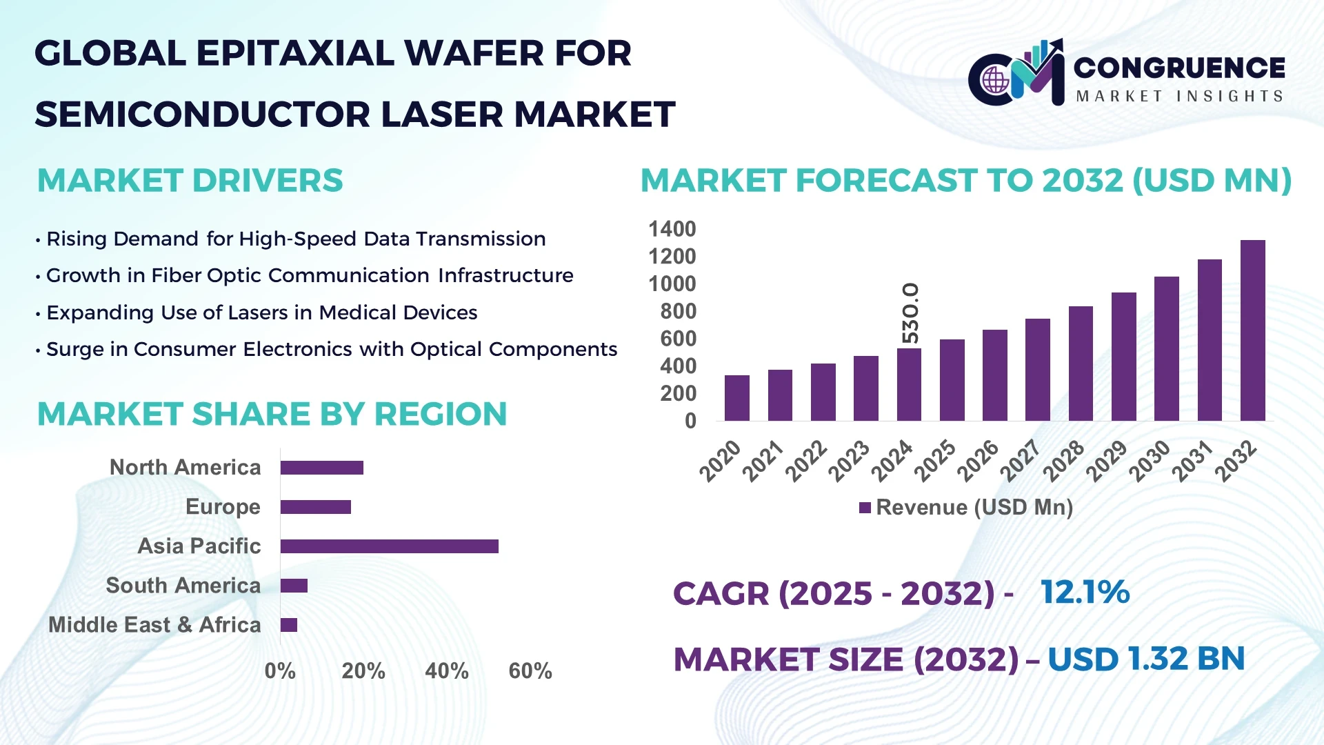
The Global Epitaxial Wafer for Semiconductor Laser Market was valued at USD 530.0 Million in 2024 and is anticipated to reach a value of USD 1321.7 Million by 2032 expanding at a CAGR of 12.1% between 2025 and 2032.
To Learn More About This Report, Request A Free Sample Copy
China continues to dominate this segment, accounting for over 45% of global shipments in 2024, fueled by its robust semiconductor ecosystem and aggressive investment in photonics and laser manufacturing infrastructure. The country's vertically integrated supply chains and favorable government subsidies provide a competitive edge in epitaxial wafer fabrication for laser applications.
The market is witnessing rapid advancements in wafer diameter scaling—from 4‑ to 6‑inch GaAs substrates—enabling higher throughput and lower per‑unit costs. Additionally, precision improvements in layer uniformity and defect control are reducing device failure rates by up to 30% compared to earlier generations, directly enhancing yield and cost‑efficiency in laser component production.
AI is revolutionizing epitaxial wafer production for semiconductor lasers by embedding intelligent control systems across the wafer fabrication process. Advanced machine learning algorithms are now routinely deployed to monitor growth conditions in real time—adjusting critical parameters like temperature, pressure, and precursor flow within milliseconds to correct anomalies before defects form. This has led to a notable 20% reduction in dislocation density across GaAs and InP wafers, directly boosting device reliability and performance.
In metrology, AI-powered optical inspection tools can now detect sub‑micron defects on wafer surfaces with over 95% accuracy, significantly surpassing human inspectors. These systems also analyze complex patterns of wafer non‑uniformity, generating predictive alerts that help avoid costly batch rejections.
Moreover, AI-driven yield optimization platforms analyze historical and live fab data, applying predictive analytics to forecast failure points. Manufacturers leveraging these tools have reported yield improvements between 8–12%, translating into millions of dollars in recovered value per production line annually. Cross‑fab benchmarking dashboards, powered by AI, enable rapid identification of process inefficiencies and adoption of best practices across global sites.
Smart scheduling systems further optimize tool allocation and production timelines based on AI‑derived models of machine availability and fab utilization rates. This reduced cycle time variance by approximately 15%, resulting in smoother throughput and better capacity utilization.
AI integration extends into supply chain logistics as well: intelligent demand forecasting platforms assess global laser demand, material lead times, and pricing trends, refining procurement strategies and reducing inventory costs by up to 10%. Real‑time visibility into raw material quality and supplier performance via AI monitoring helps mitigate downstream contamination risks.
By employing these AI applications collectively, epitaxial wafer manufacturers are enhancing process stability, reducing waste, improving yields, and accelerating time‑to‑market—all with measurable improvements in process KPIs.
“In 2025, IQE and Quintessent have created the world’s first scaled quantum‑dot epitaxial wafer supply chain capable of supporting production quantities. This collaboration supports the transition from copper to optical interconnects in AI data centers, enabling hundreds of millions of high‑performance edge‑emitting laser and semiconductor optical amplifier epitaxial wafers per year, with enhanced temperature performance, wall‑plug efficiency, and production uniformity.”
The exponential growth of AI workloads and high-performance computing has led to skyrocketing demand for high-bandwidth, low-latency optical interconnects. These systems rely heavily on epitaxial layers that support quantum-dot and edge-emitting lasers optimized for data center environments. Manufacturers report that demand for AI-grade epitaxial wafers rose by over 35% in 2024 alone compared to 2023. This surge is projected to continue as computing models grow in parameter size, requiring proportionally higher optical I/O density and improved signal integrity. This driver is underpinned by strategic partnerships and product roadmaps that align epitaxy foundries with AI hardware OEMs and cloud hyperscalers.
Building and upgrading MOCVD or MBE production lines for epitaxial wafer fabrication demands hundreds of millions in capital investment, including strict cleanroom and infrastructure standards. Equipment costs alone for a 6-inch GaAs MOCVD cluster can exceed USD 40 million. Small and mid-size players find it increasingly challenging to compete due to rising barrier-to-entry costs, design complexity, and stringent process qualifications imposed by hyperscalers and military-grade device standards. As a result, the industry is becoming more consolidated, limiting innovation diversity but gaining reliability and scalability.
Emerging quantum-dot and nano-ridge laser epitaxial stacks offer superior temperature stability, lower threshold currents, and higher energy efficiency. Nano-ridge lasers on silicon have demonstrated continuous-wave operation at room temperature with threshold currents as low as 5 mA and output powers exceeding 1 mW. These advancements unlock new applications in fiber optic communications, AI accelerators, LiDAR, and edge sensing platforms. Foundries investing in these architectures can command premium pricing and capture emerging markets seeking low-power, high-performance laser sources.
Scaling epitaxial processes from pilot to high-volume manufacturing introduces yield and uniformity challenges. Controlling defect densities, thickness uniformity, and alloy composition across 6-inch wafers—especially for complex stacks like quantum dots—requires meticulous process engineering. Even slight deviations can render entire wafers out-of-spec, leading to per-lot yield losses of up to 12%. Process variability due to equipment maintenance cycles, precursor purity, or thermal gradients can disproportionately impact high-mix, low-volume runs, complicating cost forecasting and capacity planning.
Scale-Up of Wafer Diameters: The industry is increasingly shifting from 4-inch to 6-inch GaAs and InP wafers to exploit economies of scale. This scale-up reduces cost per die by roughly 25–30%, enabling manufacturers to better compete on pricing and throughput. Equipment vendors are responding with high-throughput reactors and improved gas flow design to maintain uniform layer deposition.
Quantum-Dot and Nano-Ridge Dominance: Adoption of quantum-dot laser stacks is accelerating due to their enhanced temperature stability, lower threshold currents, and improved lifetime performance. Nano-ridge III‑V lasers directly grown on silicon platforms are gaining traction for next-generation photonics. Production-grade wafers now regularly exhibit threshold currents as low as 5 mA and output powers in the milliwatt range, making them viable for embedded applications.
Vertical Integration with Silicon Photonics: Integration of III‑V epitaxial layers onto silicon photonics platforms is narrowing. Embedded III‑V lasers grown directly on SOI substrates are achieving room‑temperature continuous‑wave operation, enabling fully monolithic photonic integrated circuits. This trend is unlocking new value in terms of chip-level optical integration, lower packaging costs, and higher bandwidth densities required by AI interconnects.
Rise of AI-Driven Process Control: Manufacturers are embedding AI agents across wafer fab tools—from MOCVD to optical metrology—to automate decision-making in real time. Defect detection accuracy has surpassed 95%, and process drift is spontaneously corrected within seconds. Fab managers report yield improvements of 8–12% and a 15% reduction in downtime, reflecting the operational impact of AI adoption across the board.
The Global Epitaxial Wafer for Semiconductor Laser Market demonstrates a diverse segmentation landscape across Type, Application, and End-User categories. Each segment is evolving uniquely in response to shifting technology demands and market trends. By Type, advancements in material engineering are driving innovation in Gallium Arsenide (GaAs), Indium Phosphide (InP), Gallium Nitride (GaN), and Silicon-based wafers. In Application, Telecommunications and Data Communication continue to dominate, though Sensing and Medical Lasers are rapidly gaining momentum. Among End-Users, the Telecommunications industry leads in volume, while the AI-driven Data Center segment is expanding at a faster pace due to rising demand for optical interconnects. These segmentation dynamics collectively reflect how the market is evolving to meet the needs of high-growth verticals like AI, LiDAR, and photonics integration.
The Epitaxial Wafer for Semiconductor Laser Market is segmented into Gallium Arsenide (GaAs), Indium Phosphide (InP), Gallium Nitride (GaN), and Silicon-based epitaxial wafers. GaAs epitaxial wafers continue to lead the market, accounting for approximately 52% of global revenue in 2024. They are the material of choice for red and near-infrared lasers used extensively in consumer electronics, optical storage, and telecommunications. InP wafers represent the fastest growing segment, with demand surging by over 18% year-on-year due to their superior performance in high-speed data communication and long-wavelength laser applications. InP’s inherent compatibility with silicon photonics is fueling this growth, as hyperscale data centers adopt InP-based lasers for next-gen optical transceivers. Meanwhile, GaN epitaxial wafers are gaining traction in emerging applications like LiDAR, UV curing, and medical lasers. Silicon-based wafers remain niche but are crucial in hybrid integration strategies where cost and scalability are prioritized. The ongoing material innovations across these types are reshaping competitive dynamics in the market.
The Epitaxial Wafer for Semiconductor Laser Market serves a diverse array of applications, including Telecommunications, Data Communication, Sensing, Medical Lasers, Consumer Electronics, and Industrial Processing. Telecommunications remains the largest application segment, driven by the ongoing rollout of 5G networks and optical fiber expansion. This segment accounted for nearly 40% of market revenue in 2024. However, Data Communication is the fastest growing segment, expanding by over 20% annually. The explosive rise of AI workloads and hyperscale data centers is fueling demand for high-bandwidth, low-latency optical interconnects, where semiconductor lasers built on InP and GaAs epitaxial wafers play a critical role. Sensing applications—including LiDAR for autonomous vehicles and industrial robotics—are also witnessing robust growth, with shipments doubling over the past two years. Medical Lasers, particularly in dermatology and ophthalmology, are adopting advanced epitaxial wafers to enable miniaturized, high-efficiency laser modules. This multi-application dynamism is driving steady demand diversification across the market.
The market’s End-User landscape includes Telecommunications Providers, Data Center Operators, Consumer Electronics Manufacturers, Automotive OEMs, Healthcare Providers, and Industrial Equipment Manufacturers. Telecommunications Providers lead the market, accounting for about 38% of global wafer consumption, driven by ongoing investments in optical network infrastructure and metro/core fiber deployments. However, Data Center Operators represent the fastest growing End-User segment, with epitaxial wafer demand rising sharply as AI and cloud computing fuel the need for advanced optical links. Data centers are increasingly deploying InP-based lasers and hybrid silicon photonic solutions to overcome electrical interconnect bottlenecks. Consumer Electronics Manufacturers maintain a stable share, particularly in facial recognition, 3D sensing, and AR/VR applications. Automotive OEMs are emerging as a strategic growth vertical, with LiDAR-based sensing driving demand for GaAs and GaN wafers. Healthcare Providers are leveraging high-efficiency semiconductor lasers for minimally invasive procedures. The cross-sector adoption of semiconductor lasers is broadening the market’s End-User base and creating new innovation pathways.
Asia-Pacific accounted for the largest market share at 52.4% in 2024; however, North America is expected to register the fastest growth, expanding at a CAGR of 13.7% between 2025 and 2032.
To Learn More About This Report, Request A Free Sample Copy
The Asia-Pacific region leads due to the concentration of major epitaxial wafer fabs in China, Japan, South Korea, and Taiwan, supported by government incentives and robust semiconductor ecosystems. North America’s rapid growth is fueled by AI-driven optical interconnect demand and leadership in quantum-dot laser R&D. Europe maintains a strong presence in automotive LiDAR and defense lasers, while emerging markets in South America and the Middle East & Africa are starting to leverage semiconductor lasers for industrial and medical applications.
AI Workloads Driving Demand for Next-Gen Optical Interconnects
In North America, the demand for epitaxial wafers is strongly linked to the exponential growth of AI-driven data centers. U.S.-based hyperscalers are rapidly scaling optical interconnect capacity, which is pushing demand for InP-based epitaxial wafers for high-performance data center transceivers. In 2024, the region accounted for 23.6% of global wafer consumption. Additionally, advancements in silicon photonics integration, led by U.S. tech companies, are boosting requirements for hybrid epitaxial stacks. The market is also seeing rising demand for GaAs wafers in consumer electronics, driven by facial recognition and AR/VR device sales. Strategic partnerships between wafer manufacturers and U.S. OEMs are accelerating technology cycles in the region.
Automotive LiDAR and Defense Sectors Fueling Growth
Europe’s epitaxial wafer market is primarily driven by strong demand from the automotive and defense sectors. In 2024, Europe represented 14.8% of global market share. Germany and France are leading adopters of GaAs and GaN-based wafers for LiDAR systems used in autonomous vehicles. European automakers are prioritizing LiDAR integration, with shipments of automotive LiDAR units increasing by 48% year-over-year. In parallel, European defense programs are heavily investing in next-gen laser-based systems for targeting, communications, and countermeasures, driving demand for high-performance InP epitaxial wafers. The region’s focus on sustainability is also spurring interest in energy-efficient laser components across industrial applications.
Dominance in High-Volume Manufacturing and Supply Chain Integration
Asia-Pacific continues to dominate the global market, holding 52.4% share in 2024. China leads wafer production with aggressive government support for photonics and laser technology, controlling over 45% of the regional output. Japan and South Korea are key innovators in precision epitaxy for GaN and InP wafers, catering to high-end optical communication and sensing applications. Taiwan’s foundry ecosystem is integrating epitaxial wafer capacity to support the rising demand for silicon photonics. The Asia-Pacific market benefits from vertically integrated supply chains, allowing faster innovation cycles and lower production costs. Demand is also strong in consumer electronics, where smartphone OEMs source advanced GaAs wafers for 3D sensing modules.
Emerging Medical Laser Applications and Industrial Adoption
The South American market, while smaller in scale, is witnessing notable growth in medical and industrial laser applications. In 2024, the region captured 3.1% of global market share. Brazil leads the market with increasing imports of GaAs and InP wafers for medical devices used in dermatology, ophthalmology, and dental procedures. The region is also adopting semiconductor lasers for industrial material processing, including metal cutting and welding, where precision and efficiency are critical. Government-led modernization initiatives in manufacturing are further supporting the uptake of laser-based technologies. Supply chain challenges remain, but localized demand is prompting partnerships with Asian and European wafer suppliers.
Defense and Oil & Gas Sector Demands Catalyzing Adoption
The Middle East & Africa region accounted for 2.7% of global market share in 2024. Demand is driven by specialized applications in defense and the oil & gas sectors. Countries like Israel and the UAE are investing heavily in directed energy weapons and laser-based communication systems, increasing demand for high-performance InP epitaxial wafers. In the oil & gas industry, GaN and InP wafers are being utilized in laser-based pipeline inspection and exploration tools. Medical laser markets are also emerging in the region, with hospitals adopting semiconductor lasers for minimally invasive surgeries. Supply chain constraints persist, but strategic collaborations with global wafer suppliers are addressing these gaps.
China - valued at approx. 41%, it's leadership stems from its integrated photonics supply chain and large-scale manufacturing capacity
The competitive landscape for the Epitaxial Wafer for Semiconductor Laser market is shaped by a small group of global leaders, each commanding strong capabilities in epitaxial growth, advanced MOCVD and MBE processes, and integrated ecosystem support. Companies such as IQE, Jenoptik Diode Lab, Coherent, Shin‑Etsu, and SUMCO dominate the high end of the value chain, offering 300 mm wafer capacity and proprietary low‑defect technologies. For instance, Shin‑Etsu operates five 300 mm epitaxial lines producing over 4.2 million wafers annually, securing a substantial share of the global supply. SUMCO has expanded its 300 mm wafer output with ultra-flat and ultra-low-resistivity product lines adopted by major foundries in South Korea and Taiwan, boosting demand by approximately 17% since 2023.
Small and mid-tier specialist fabs, such as Intelliepi and Jenoptik, focus on tailored quantum-dot and nano-ridge lasers, catering to niche laser-device manufacturers. Consolidation has been active: several mergers and acquisitions have occurred to access technology and capacity—particularly seen in the AI data-center supply chain. Moderate competition combined with high technical barriers keeps market power concentrated among a handful of providers, even as innovation continues through partnerships in quantum-dot, hybrid silicon photonics, and AI-optimized process control.
Overall, competition remains specialized. The largest suppliers compete on wafer size, defect density, and integrated supply chain support; mid-tier players differentiate based on material expertise or application-specific stacks. A trend toward strategic alliances with device OEMs (e.g. data center, automotive LiDAR, medical laser vendors) is further influencing market positioning.
IQE
Jenoptik Diode Lab
Coherent
Shin‑Etsu
SUMCO
Intelliepi
LUMIBIRD
Riber
Technological advancements in epitaxial wafer production are advancing both process control and material innovation. MOCVD remains the primary commercial technique, favored for its scalability and quality control. Recent developments include halogen-free vapor-phase epitaxy systems, which reduce environmental impact while maintaining high throughput and material uniformity.
The move to 300 mm wafers has accelerated—Shin‑Etsu’s new fab is expected to produce 1.8 million epitaxial wafers annually from Q3 2024, while SUMCO has enhanced its 300 mm product lines to support next-gen transistor structures and low-resistivity requirements. These expansions underline a shift toward large-diameter platforms aligned with advanced logic and photonics integration.
On defect metrology, equipment like DualBeam tools combining FIB and SEM enables nanoscale inspection and automated workflows, substantially reducing throughput bottlenecks. Similarly, AI‑driven defect detection in MOCVD and optical inspection systems is improving yield and identifying process drift in real time.
Material stack innovations include development of GaN, InP, and quantum-dot stacks tailored for nano‑ridge and silicon-integrated lasers. A breakthrough demonstration reported full CMOS-line fabrication of 300 mm GaAs nano-ridge lasers with threshold currents as low as 5 mA and output powers over 1 mW. Additionally, wafer-scale InGaP-on-insulator substrates have been realized for nonlinear and quantum photonic applications, achieving resonator Q-factors above 300,000.
Overall, the technology trajectory centers on larger wafer sizes, ultra-low defect densities, AI-enhanced process controls, and novel material platforms enabling monolithic laser integration for a wider range of end-products.
In January 2024, Innolume ordered a state-of-the-art MBE‑49 system to significantly expand GaAs quantum-dot laser production capacity, aiming to support consumer electronics and data communications supply chains.
In January 2024, Coherent launched a VCSEL-based illumination module targeted at short‑ and mid-range LiDAR, innovating stack design for automotive and industrial 3D sensing.
In early 2024, IQE appointed a new CFO and VP of Government Affairs, highlighting their strategic focus on scaling fabs and leveraging public-sector funding.
In Q3 2023, SUMCO released ultra-flat 300 mm epitaxial wafers with resistivity under 0.005 Ω·cm and edge exclusion within 1.5 mm—features quickly adopted by South Korean and Taiwanese foundries, increasing demand by roughly 17%.
This market report delivers an expansive yet concise overview of the global Epitaxial Wafer for Semiconductor Laser industry. It examines wafer types (GaAs, InP, GaN, Silicon), application sectors (Telecom, Data Centers, Sensing, Medical, Industrial, Consumer), and regional dynamics (Asia-Pacific, North America, Europe, rest of world). The report provides company profiling, technology insights, process innovations, and the competitive landscape.
It focuses on material and process evolution including 300 mm wafer adoption, quantum-dot and nano-ridge architectures, AI-optimized MOCVD, defect metrology, and hybrid/bonded silicon photonics platforms. The analysis includes detailed regional trends and highlights contributing OEMs and integrators across industries (hyperscalers, automotive, healthcare).
Additionally, the report outlines recent technological and company developments—such as new fab capacity, advanced inspection tools, and stack-level innovations like VCSEL and hybrid lasers. Stakeholders gain actionable information to inform investment, strategic planning, and competitive positioning. The content is tailored for C-level executives, technology strategists, investors, and R&D professionals seeking high-level synthesis and focal insights into an evolving down-stream value chain.
| Report Attribute / Metric | Report Details |
|---|---|
| Market Name | Global Epitaxial Wafer for Semiconductor Laser Market |
| Market Revenue (2024) | USD 530.0 Million |
| Market Revenue (2032) | USD 1,321.7 Million |
| CAGR (2025–2032) | 12.1% |
| Base Year | 2024 |
| Forecast Period | 2025–2032 |
| Historic Period | 2020–2024 |
| Segments Covered |
By Type
By Application
By End-User
|
| Key Report Deliverables | Revenue Forecast, Growth Trends, Market Dynamics, Segmental Overview, Regional and Country-wise Analysis, Competition Landscape, Technological Insights, Recent Developments |
| Regions Covered | North America, Europe, Asia-Pacific, South America, Middle East & Africa |
| Key Players Analyzed | IQE, Jenoptik Diode Lab, Coherent, Shin‑Etsu, SUMCO, Intelliepi, LUMIBIRD, Riber |
| Customization & Pricing | Available on Request (10% Customization is Free) |


