
Reports
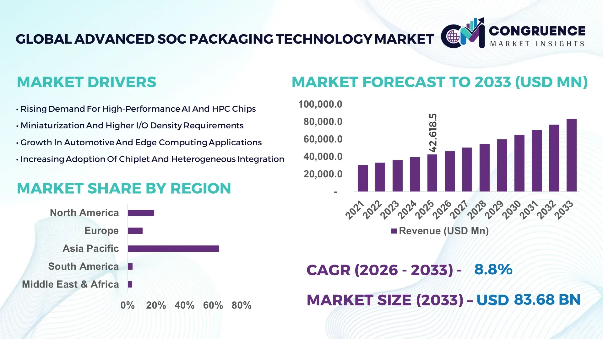
The Global Advanced SoC Packaging Technology Market was valued at USD 42,618.5 Million in 2025 and is anticipated to reach a value of USD 83,681.5 Million by 2033 expanding at a CAGR of 8.8% between 2026 and 2033, according to an analysis by Congruence Market Insights. Growth is driven by rising demand for high-performance computing, AI accelerators, and compact semiconductor architectures.
Taiwan dominates the Advanced SoC Packaging Technology market through large-scale advanced packaging capacity, sustained semiconductor investments, and leadership in high-density chip integration. In 2025, Taiwanese facilities processed more than 14 million advanced packaged wafers, supported by over USD 22 billion in annual capital expenditure across 2.5D and 3D packaging lines. High-performance computing and AI processors accounted for nearly 48% of advanced packaging demand, while smartphone SoC packaging represented around 31%. Over 65% of new advanced packaging lines deployed in the country supported chiplet-based architectures and high-bandwidth memory integration, reflecting strong technological advancement and manufacturing scale.
Market Size & Growth: Valued at USD 42,618.5 million in 2025, projected to reach USD 83,681.5 million by 2033 at 8.8% CAGR, driven by demand for AI and high-performance computing chips.
Top Growth Drivers: AI chip adoption (52%), chiplet-based architectures (44%), high-bandwidth memory integration (36%).
Short-Term Forecast: By 2028, advanced packaging is expected to improve chip performance-per-watt by 28%.
Emerging Technologies: 2.5D interposers, 3D stacked chiplets, fan-out wafer-level packaging.
Regional Leaders: Asia Pacific projected at USD 48.2 billion by 2033 with foundry expansion; North America at USD 19.6 billion driven by AI chip demand; Europe at USD 11.4 billion supported by automotive semiconductor growth.
Consumer/End-User Trends: Over 57% of advanced packaged chips are deployed in AI servers, smartphones, and automotive electronics.
Pilot or Case Example: In 2024, an advanced packaging pilot reduced signal latency by 22% using 3D stacked chiplets.
Competitive Landscape: TSMC leads with about 32% share, followed by ASE Technology, Amkor Technology, Intel, and Samsung Electronics.
Regulatory & ESG Impact: Semiconductor localization incentives and energy-efficiency standards influencing packaging investments.
Investment & Funding Patterns: More than USD 120 billion invested globally between 2023–2025 in advanced packaging and semiconductor back-end facilities.
Innovation & Future Outlook: Integration of chiplet architectures, photonic interconnects, and heterogeneous integration shaping next-generation packaging.
High-performance computing accounts for nearly 38% of advanced packaging demand, followed by smartphones at 29% and automotive electronics at 18%. Innovations in chiplet-based designs, fan-out wafer-level packaging, and high-bandwidth memory integration are improving computing density and energy efficiency. Government semiconductor incentives, AI server expansion, and electric vehicle electronics demand are key drivers shaping regional growth patterns and future market outlook.
The Advanced SoC Packaging Technology Market is strategically critical as semiconductor scaling shifts from transistor-level improvements to advanced integration and packaging architectures. With transistor miniaturization approaching physical limits, chiplet-based designs and 3D stacking are enabling performance gains without relying solely on smaller process nodes. 3D stacked chiplet packaging delivers up to 35% performance improvement compared to traditional monolithic SoC designs, while reducing interconnect latency and power consumption.
From a regional perspective, Asia-Pacific dominates in volume due to concentrated semiconductor manufacturing ecosystems, while North America leads in adoption with over 61% of AI chip developers using advanced packaging technologies. By 2028, heterogeneous integration platforms are expected to reduce system-level power consumption by 26%, enabling more efficient AI servers and edge computing devices.
Sustainability and compliance considerations are also shaping investment strategies. Semiconductor firms are committing to ESG targets such as 30% reductions in packaging material waste and 25% improvements in energy efficiency across packaging facilities by 2030. In 2024, a leading Asian packaging facility achieved a 21% reduction in process energy consumption through AI-optimized thermal management systems.
Future pathways emphasize photonic interconnects, wafer-level packaging, and chiplet-based architectures for AI, automotive, and data center applications. By 2027, advanced packaging is expected to improve AI accelerator throughput by 33%. These developments position the Advanced SoC Packaging Technology Market as a pillar of semiconductor innovation, supply chain resilience, and sustainable high-performance computing growth.
The Advanced SoC Packaging Technology market is shaped by rapid growth in AI workloads, high-performance computing demand, and the transition toward heterogeneous integration. As traditional transistor scaling slows, semiconductor manufacturers are focusing on advanced packaging techniques such as 2.5D interposers, fan-out wafer-level packaging, and 3D stacked chiplets. These technologies enable higher transistor density, improved signal integrity, and reduced power consumption. Demand is increasing across AI servers, smartphones, automotive electronics, and edge computing devices. Government incentives for semiconductor manufacturing, coupled with strategic investments in advanced packaging facilities, are further accelerating market expansion.
The rapid expansion of AI workloads and high-performance computing applications is a primary driver for the Advanced SoC Packaging Technology market. AI training processors now contain over 100 billion transistors, requiring advanced packaging solutions to maintain performance and power efficiency. In 2025, more than 58% of AI accelerator chips utilized advanced packaging techniques such as 2.5D interposers or 3D stacking. These architectures improve data transfer speeds by up to 40% while reducing power consumption by 25%, making them essential for next-generation computing platforms.
Advanced packaging facilities require significant capital investment in specialized equipment, cleanroom infrastructure, and precision assembly tools. Building a single advanced packaging line can cost over USD 1 billion, limiting entry for smaller players. Additionally, advanced packaging processes involve complex materials and high defect sensitivity, increasing operational costs. In 2025, nearly 31% of semiconductor firms cited high capital expenditure as a barrier to scaling advanced packaging capacity.
Chiplet-based architectures present a major growth opportunity by enabling modular chip designs and improved yield rates. Instead of manufacturing a single large die, manufacturers can combine multiple smaller chiplets using advanced packaging. This approach improves production yields by up to 18% and reduces development costs for complex processors. In 2025, over 46% of new AI and high-performance computing chips were designed using chiplet-based architectures, highlighting the expanding opportunity for advanced packaging providers.
Advanced packaging technologies increase power density, creating significant thermal management challenges. 3D stacked chip architectures can raise localized temperatures by up to 15°C compared to conventional designs. Managing heat dissipation while maintaining signal integrity requires advanced materials and cooling solutions. Additionally, integration complexity increases defect risks, with multi-die packages requiring precision alignment at micron-level tolerances. These technical challenges raise production complexity and operational costs.
Expansion of 3D Stacked Chiplet Architectures: In 2025, more than 42% of AI accelerators used 3D stacked chiplet packaging, improving data transfer speeds by 37% and reducing interconnect latency by 29%.
Growth of Fan-Out Wafer-Level Packaging: Fan-out packaging accounted for nearly 34% of advanced SoC packages in 2024, enabling up to 22% thinner package profiles and 18% better electrical performance.
Integration of High-Bandwidth Memory in AI Chips: Over 48% of new AI server processors launched in 2025 incorporated high-bandwidth memory within advanced packages, increasing memory bandwidth by 2.5× compared to traditional configurations.
Rise of Heterogeneous Integration Platforms: Approximately 39% of new high-performance computing chips deployed heterogeneous integration, combining logic, memory, and specialized accelerators within a single advanced package, improving performance-per-watt by 31%.
The Advanced SoC Packaging Technology market is segmented by packaging type, application, and end-user industries. Segmentation reflects the diverse performance and integration requirements across computing platforms. Packaging types include fan-out wafer-level packaging, 2.5D interposers, and 3D stacked chiplets. Applications span smartphones, AI servers, automotive electronics, and consumer devices. End-user demand varies across semiconductor manufacturers, cloud providers, and automotive OEMs, with performance, power efficiency, and miniaturization serving as primary decision factors.
Fan-out wafer-level packaging accounts for approximately 38% of adoption due to its thin profile and cost efficiency for high-volume smartphone and consumer chip applications. 2.5D interposer-based packaging holds about 29%, primarily used in high-performance computing and AI accelerators. However, 3D stacked chiplet packaging is the fastest-growing segment, expected to expand at over 11% CAGR, driven by demand for AI servers and advanced processors. Other packaging types, including system-in-package and embedded multi-die interconnect bridge solutions, collectively represent 33% of adoption.
In 2025, a national semiconductor program deployed advanced fan-out packaging for over 120 million smartphone processors, improving power efficiency by 16%.
Smartphones remain the leading application with a 29% share, driven by demand for compact, high-performance SoC designs. AI servers represent the fastest-growing segment, expanding above 12% CAGR as cloud and data center investments accelerate. Automotive electronics and edge computing applications collectively account for 41% of demand, reflecting increasing semiconductor content in vehicles and IoT devices. In 2025, more than 48% of AI processors deployed advanced packaging technologies.
In 2024, advanced packaging was implemented across over 3,500 AI server clusters, improving data throughput by 24%.
Semiconductor manufacturers represent the leading end-user segment at 52%, reflecting their central role in chip production and integration. Cloud service providers are the fastest-growing end-user group, expanding at over 13% CAGR as AI infrastructure scales. Automotive OEMs, consumer electronics brands, and telecom equipment manufacturers collectively represent 48% of demand. In 2025, more than 44% of data center operators deployed servers with advanced packaged processors.
In 2025, a national data center expansion program deployed advanced packaged processors across 1,800 AI server facilities, improving compute efficiency by 27%.
Asia-Pacific accounted for the largest market share at 64.3% in 2025 however, North America is expected to register the fastest growth, expanding at a CAGR of 9.6% between 2026 and 2033.
Asia-Pacific processed more than 28 million advanced packaged wafers in 2025, with Taiwan, South Korea, China, and Japan collectively contributing over 81% of global advanced packaging output. North America accounted for 18.7% of total demand, driven by AI server deployments exceeding 1.9 million units and advanced packaging adoption across high-performance computing chips. Europe represented 10.4%, supported by automotive semiconductor demand, where over 46% of new electric vehicle control units used advanced packaged SoCs. South America held 3.2% of global demand, primarily from telecom and consumer electronics assembly hubs. Middle East & Africa accounted for 3.4%, with semiconductor packaging demand growing in data center infrastructure and industrial automation projects.
How is AI chip demand accelerating heterogeneous integration adoption?
North America accounted for approximately 18.7% of the Advanced SoC Packaging Technology market in 2025, supported by strong demand from AI, cloud computing, and defense electronics sectors. Over 61% of AI accelerator chips deployed in regional data centers used advanced packaging technologies such as 2.5D interposers or 3D stacked chiplets. Government semiconductor incentives and manufacturing support programs encouraged domestic advanced packaging capacity expansion. Technological trends include chiplet-based architectures, high-bandwidth memory integration, and photonic interconnect research. A regional semiconductor company expanded advanced packaging facilities capable of processing over 600,000 AI chips annually. Consumer behavior in the region reflects high enterprise adoption across cloud computing, healthcare, and financial technology sectors.
Why are automotive electronics and sustainability goals driving advanced packaging adoption?
Europe represented approximately 10.4% of the Advanced SoC Packaging Technology market in 2025, with Germany, France, and the UK accounting for nearly 67% of regional semiconductor demand. Automotive electronics remain a major driver, with over 46% of new electric vehicle control systems integrating advanced packaged SoCs. Regulatory bodies have introduced sustainability targets for semiconductor manufacturing, encouraging energy-efficient packaging processes. Adoption of heterogeneous integration and chiplet-based designs increased across automotive and industrial automation applications. A European semiconductor manufacturer launched advanced packaging lines for automotive processors, increasing output capacity by 22%. Consumer behavior is shaped by regulatory pressure, leading to demand for energy-efficient and reliable semiconductor solutions.
What is enabling large-scale advanced packaging capacity across semiconductor hubs?
Asia-Pacific led the global Advanced SoC Packaging Technology market in 2025, processing more than 28 million advanced packaged wafers across major semiconductor hubs. Taiwan, South Korea, China, and Japan together represented over 81% of regional output. Infrastructure investments exceeding USD 60 billion supported new packaging plants and equipment upgrades. Technology clusters in Taiwan and South Korea focus on 3D stacking, fan-out wafer-level packaging, and high-bandwidth memory integration. A regional packaging leader expanded its advanced packaging capacity by 35%, enabling support for next-generation AI processors. Consumer behavior in the region reflects strong demand from smartphone, AI server, and automotive electronics manufacturers.
How are telecom and consumer electronics assembly hubs shaping packaging demand?
South America accounted for approximately 3.2% of global Advanced SoC Packaging Technology demand in 2025, led by Brazil and Argentina. Brazil represented over 58% of regional semiconductor packaging activity, supported by consumer electronics assembly and telecom infrastructure expansion. Government trade policies reduced import duties on semiconductor components by up to 10% to encourage local manufacturing. A regional electronics manufacturer partnered with a packaging service provider to deploy advanced packaged SoCs across 2.4 million consumer devices. Consumer behavior in the region is influenced by rising smartphone penetration and demand for affordable electronics.
Why are data center investments increasing advanced semiconductor packaging demand?
The Middle East & Africa region accounted for approximately 3.4% of global Advanced SoC Packaging Technology demand in 2025, with UAE and South Africa leading adoption. Data center investments across Gulf countries exceeded USD 12 billion, driving demand for advanced packaged processors. Industrial automation and telecom infrastructure projects also increased semiconductor usage. A regional technology integrator deployed advanced packaged SoCs across more than 140 data center facilities, improving compute efficiency by 18%. Consumer behavior reflects premium adoption in Gulf markets and cost-efficient electronics demand across emerging African economies.
Taiwan Advanced SoC Packaging Technology Market – 29.6%: High advanced packaging capacity and strong integration with global semiconductor supply chains.
United States Advanced SoC Packaging Technology Market – 18.2%: Strong demand from AI, cloud computing, and defense electronics sectors.
The Advanced SoC Packaging Technology market is moderately consolidated, with approximately 40 major global players and several regional specialists competing across high-performance computing, smartphone, and automotive segments. The top five companies collectively account for nearly 69% of total advanced packaging capacity, supported by large-scale capital investments and proprietary packaging technologies. Leading firms focus on chiplet-based integration, 3D stacking, and high-bandwidth memory solutions to differentiate their offerings.
Between 2023 and 2025, over 25 new advanced packaging facilities were announced globally, with combined investments exceeding USD 100 billion. Strategic partnerships between foundries, OSAT providers, and AI chip developers increased by 31% during the same period. Product innovation cycles are accelerating, with new packaging platforms introduced every 18–24 months to support higher transistor densities and improved power efficiency. Competitive positioning is increasingly defined by packaging throughput, yield rates, and integration capabilities, particularly in AI and data center applications.
Taiwan Semiconductor Manufacturing Company (TSMC)
ASE Technology Holding
Amkor Technology
Intel Corporation
Samsung Electronics
JCET Group
Powertech Technology Inc.
Tongfu Microelectronics
STATS ChipPAC
UTAC Holdings
Nepes Corporation
ChipMOS Technologies
Technological evolution in the Advanced SoC Packaging Technology market is driven by heterogeneous integration, chiplet-based architectures, and advanced interconnect solutions. Modern 2.5D interposer technologies enable data transfer rates exceeding 2 terabits per second between chiplets, significantly improving processing performance. 3D stacked packaging increases transistor density by up to 45% compared to conventional single-die designs, enabling compact high-performance computing solutions.
Fan-out wafer-level packaging is gaining traction, offering up to 22% thinner package profiles and improved electrical performance for mobile and consumer electronics. High-bandwidth memory integration is also advancing, with new packaging platforms supporting memory bandwidth improvements of more than 2.5 times compared to traditional designs. Thermal interface materials and advanced cooling solutions are improving heat dissipation by up to 30%, addressing challenges associated with higher power densities.
Emerging technologies include photonic interconnects, which can reduce signal latency by up to 40% compared to electrical interconnects, and embedded multi-die interconnect bridges that enable flexible chiplet integration. These technologies are enhancing performance-per-watt, reducing form factors, and enabling next-generation AI, automotive, and edge computing platforms.
In March 2025, Intel announced expansion of its advanced packaging capacity for chiplet-based processors, increasing production capability by over 40% to support AI and high-performance computing applications. Source: www.intel.com
In October 2024, TSMC began volume production of its next-generation 3D stacked packaging platform, enabling higher transistor density and improving performance-per-watt for AI accelerators. Source: www.tsmc.com
In July 2024, Amkor Technology introduced an advanced fan-out packaging solution supporting high-bandwidth memory integration, improving signal performance and reducing package thickness by 20%. Source: www.amkor.com
In May 2024, Samsung Electronics launched an upgraded 2.5D packaging platform for AI processors, increasing memory bandwidth by more than 2× and improving energy efficiency. Source: www.samsung.com
The Advanced SoC Packaging Technology Market Report provides a comprehensive evaluation of packaging types, applications, technologies, and end-user industries across global semiconductor markets. The scope includes fan-out wafer-level packaging, 2.5D interposers, 3D stacked chiplets, and system-in-package solutions designed for high-performance and compact electronic systems.
Applications analyzed include smartphones, AI servers, automotive electronics, consumer devices, and industrial automation platforms. Technology segments covered include heterogeneous integration, high-bandwidth memory packaging, chiplet architectures, photonic interconnects, and advanced thermal management systems. The report evaluates packaging throughput, integration density, signal performance, and power efficiency across different packaging approaches.
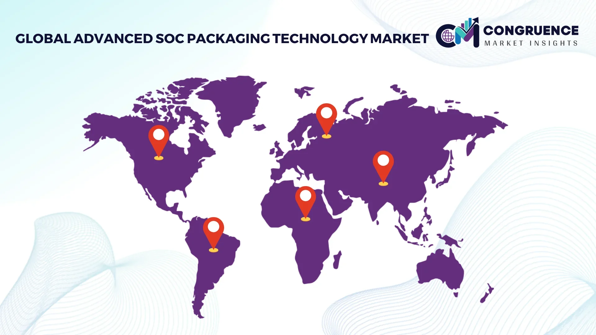
Geographic coverage includes North America, Europe, Asia-Pacific, South America, and Middle East & Africa, with country-level insights for major semiconductor manufacturing and consumption hubs. Emerging segments such as chiplet-based AI accelerators, automotive autonomous driving processors, and edge computing SoCs are also included. The report provides strategic insights into packaging capacity expansion, technology transitions, industry adoption trends, and competitive positioning relevant to semiconductor manufacturers, OSAT providers, equipment suppliers, and technology investors.
| Report Attribute/Metric | Report Details |
|---|---|
|
Market Revenue in 2025 |
USD 42,618.5 Million |
|
Market Revenue in 2033 |
USD 83,681.5 Million |
|
CAGR (2026 - 2033) |
8.8% |
|
Base Year |
2025 |
|
Forecast Period |
2026 - 2033 |
|
Historic Period |
2021 - 2025 |
|
Segments Covered |
By Type
By Application
By End-User
|
|
Key Report Deliverable |
Revenue Forecast, Growth Trends, Market Dynamics, Segmental Overview, Regional and Country-wise Analysis, Competition Landscape |
|
Region Covered |
North America, Europe, Asia-Pacific, South America, Middle East, Africa |
|
Key Players Analyzed |
Unimicron, Ibiden, Shinko Electric Industries, Taiwan Semiconductor Manufacturing Company (TSMC), ASE Technology Holding, Amkor Technology, Intel Corporation, Samsung Electronics, JCET Group, Powertech Technology Inc., Tongfu Microelectronics, STATS ChipPAC, UTAC Holdings, Nepes Corporation, ChipMOS Technologies |
|
Customization & Pricing |
Available on Request (10% Customization is Free) |


