
Reports
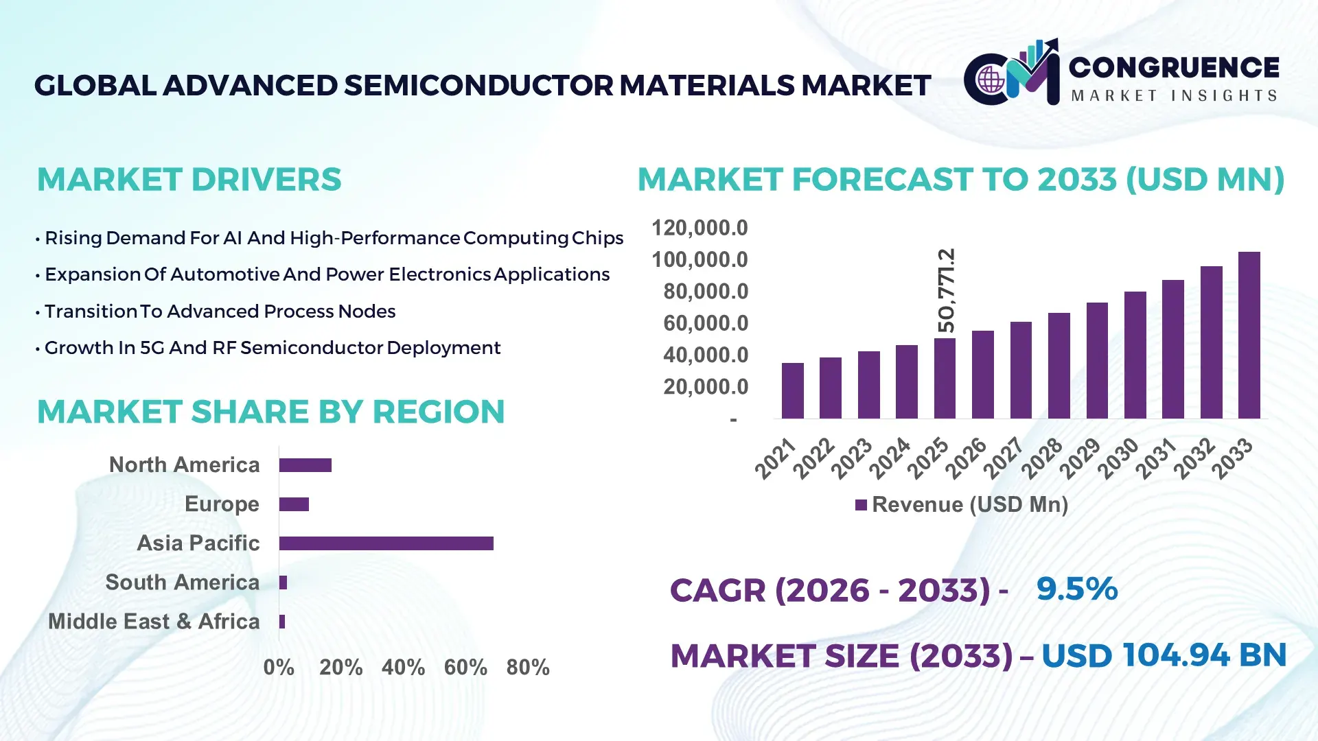
The Global Advanced Semiconductor Materials Market was valued at USD 50,771.2 Million in 2025 and is anticipated to reach a value of USD 104,937.4 Million by 2033 expanding at a CAGR of 9.5% between 2026 and 2033, according to an analysis by Congruence Market Insights. Growth is driven by rapid demand for AI processors, advanced memory chips, and high-performance computing devices.
China dominates the Advanced Semiconductor Materials market through extensive wafer fabrication capacity, large-scale investments, and expanding demand across consumer electronics, automotive, and telecommunications industries. In 2025, the country operated more than 35 advanced semiconductor fabrication plants processing over 18 million 300mm wafers annually. Public and private investments in semiconductor materials and fabrication infrastructure exceeded USD 45 billion between 2023 and 2025. Advanced logic and memory chips accounted for nearly 52% of material consumption, while automotive semiconductor applications represented around 19%. Over 63% of new fabs deployed advanced photoresists, high-purity silicon wafers, and advanced deposition materials, reflecting accelerated technological upgrades.
Market Size & Growth: Valued at USD 50,771.2 million in 2025, projected to reach USD 104,937.4 million by 2033 at 9.5% CAGR, driven by AI and high-performance computing chip demand.
Top Growth Drivers: AI chip production growth (48%), advanced memory adoption (36%), automotive semiconductor demand (28%).
Short-Term Forecast: By 2028, advanced materials are expected to improve chip energy efficiency by 22%.
Emerging Technologies: EUV photoresists, advanced dielectric materials, compound semiconductors.
Regional Leaders: Asia-Pacific projected at USD 63.5 billion by 2033 with large-scale fabs; North America at USD 21.8 billion driven by AI chips; Europe at USD 13.6 billion supported by automotive electronics.
Consumer/End-User Trends: Over 57% of advanced semiconductor materials are consumed in AI servers, smartphones, and automotive electronics.
Pilot or Case Example: In 2024, a materials optimization pilot improved wafer yield by 18% using advanced deposition materials.
Competitive Landscape: Shin-Etsu Chemical leads with around 16% share, followed by SUMCO, GlobalWafers, SK Siltron, and BASF.
Regulatory & ESG Impact: Semiconductor localization incentives and low-emission material processing standards shaping investments.
Investment & Funding Patterns: Over USD 180 billion invested globally between 2023–2025 in semiconductor fabs and materials supply chains.
Innovation & Future Outlook: Growth in compound semiconductors, EUV materials, and advanced packaging materials supporting next-generation chips.
Advanced logic materials account for approximately 44% of demand, followed by memory-related materials at 31% and compound semiconductor materials at 25%. Innovations in EUV photoresists, high-purity silicon wafers, and advanced deposition chemicals are improving chip performance and manufacturing yields. Government semiconductor incentives, AI server expansion, and electric vehicle electronics demand are shaping regional consumption patterns and long-term market outlook.
The Advanced Semiconductor Materials Market is strategically critical as chip manufacturers transition to smaller process nodes, heterogeneous integration, and high-performance computing architectures. Advanced materials such as EUV photoresists, high-k dielectrics, and compound semiconductors enable improved transistor density, faster switching speeds, and lower power consumption. EUV-based material processes deliver up to 32% improvement in patterning accuracy compared to conventional deep ultraviolet materials, enabling sub-5nm chip manufacturing.
Regionally, Asia-Pacific dominates in production volume due to extensive fabrication infrastructure, while North America leads in adoption with over 59% of AI chip developers using advanced semiconductor materials in cutting-edge nodes. By 2028, advanced dielectric materials are expected to reduce chip-level power leakage by 24%, improving energy efficiency in data center processors.
Sustainability and compliance factors are also influencing material innovation. Semiconductor firms are committing to ESG targets such as 30% reductions in chemical waste and 20% improvements in energy efficiency across material processing lines by 2030. In 2024, a leading semiconductor manufacturer achieved a 17% reduction in process emissions by switching to low-temperature deposition materials.
Future pathways emphasize compound semiconductors, EUV-compatible materials, and advanced packaging materials for AI, automotive, and edge computing applications. By 2027, gallium nitride-based materials are expected to improve power device efficiency by 28%. These developments position the Advanced Semiconductor Materials Market as a pillar of semiconductor innovation, supply chain resilience, and sustainable electronics manufacturing.
The Advanced Semiconductor Materials market is driven by increasing demand for high-performance chips across AI, automotive, consumer electronics, and telecommunications sectors. As semiconductor nodes shrink below 5nm, advanced materials are essential for maintaining performance, yield, and reliability. Materials such as EUV photoresists, high-purity silicon wafers, advanced deposition chemicals, and compound semiconductor substrates are enabling next-generation chip designs. Government incentives for semiconductor manufacturing and localization are accelerating investments in material production facilities. At the same time, rising demand for electric vehicles, AI servers, and 5G infrastructure is expanding the consumption of advanced semiconductor materials.
AI and high-performance computing processors require advanced materials to support high transistor density and thermal efficiency. Modern AI accelerators incorporate more than 100 billion transistors, increasing demand for advanced dielectric materials and high-purity wafers. In 2025, over 61% of advanced logic chips used EUV photoresists and advanced deposition materials. These materials improve patterning precision by up to 30% and reduce defect rates, enabling reliable production of sub-5nm chips.
Advanced semiconductor materials require extremely high purity levels, often exceeding 99.9999%, which increases production complexity and costs. Manufacturing high-purity silicon wafers and advanced chemicals involves specialized facilities and stringent quality controls. In 2025, nearly 28% of semiconductor manufacturers reported supply chain delays due to limited availability of ultra-high-purity materials, highlighting a major restraint.
Compound semiconductors such as gallium nitride and silicon carbide present major growth opportunities, particularly in electric vehicles and power electronics. These materials improve power efficiency by up to 35% compared to traditional silicon-based devices. In 2025, more than 22 million electric vehicles used power modules incorporating compound semiconductor materials, highlighting expanding opportunities.
The semiconductor materials supply chain is concentrated among a limited number of global suppliers, creating vulnerability to geopolitical tensions and trade restrictions. In 2025, over 72% of advanced photoresist production was concentrated in three countries, increasing supply risk. Export controls and material shortages can disrupt fabrication schedules, raising production costs and limiting capacity expansion.
Growth in EUV Photoresist Adoption: In 2025, more than 58% of advanced logic chips were produced using EUV-compatible photoresists, improving patterning precision by 31% and reducing defect rates by 19%.
Expansion of Silicon Carbide and Gallium Nitride Materials: Compound semiconductor materials accounted for nearly 27% of power device substrates in 2024, improving energy efficiency by up to 34% in electric vehicle applications.
Rising Demand for High-Purity Silicon Wafers: Over 21 million 300mm wafers were processed using advanced materials in 2025, with high-purity wafer demand increasing by 23% compared to the previous year.
Integration of Advanced Dielectric and Deposition Materials: Approximately 49% of sub-7nm chips used advanced dielectric materials in 2025, reducing power leakage by up to 24%.
The Advanced Semiconductor Materials market is segmented by material type, application, and end-user industries. Material types include silicon wafers, photoresists, advanced deposition materials, and compound semiconductor substrates. Applications span logic chips, memory devices, power electronics, and RF components. End-user demand varies across semiconductor foundries, integrated device manufacturers, and electronics OEMs, with performance, yield, and power efficiency as key decision factors.
Silicon wafers account for approximately 41% of material usage due to their central role in chip fabrication. Photoresists represent about 23%, driven by advanced lithography requirements. However, compound semiconductor materials are the fastest-growing segment, expected to expand at over 12% CAGR, supported by electric vehicle and power electronics demand. Other materials, including advanced deposition chemicals and dielectric materials, collectively represent 36% of the market.
In 2025, compound semiconductor substrates were deployed across more than 18 million power electronics devices, improving energy efficiency by 29%.
Logic chips remain the leading application with a 46% share, driven by AI processors and high-performance computing devices. Memory devices account for 29%, while power electronics is the fastest-growing application, expanding above 11% CAGR due to electric vehicle and renewable energy systems. RF and sensor applications collectively represent 25%. In 2025, over 54% of semiconductor fabs focused on advanced logic and memory nodes.
In 2024, advanced semiconductor materials were used in over 4,200 AI server clusters, improving processing efficiency by 26%.
Semiconductor foundries represent the leading end-user segment at 58%, reflecting their central role in chip production. Integrated device manufacturers are the fastest-growing segment, expanding at over 10% CAGR as companies invest in advanced fabrication nodes. Electronics OEMs and automotive chip manufacturers collectively account for 42% of demand. In 2025, more than 47% of automotive semiconductor suppliers adopted compound semiconductor materials for power devices.
In 2025, a national semiconductor initiative deployed advanced materials across 11 new fabrication plants, improving wafer yield rates by 18%.
Asia-Pacific accounted for the largest market share at 68.9% in 2025 however, North America is expected to register the fastest growth, expanding at a CAGR of 10.4% between 2026 and 2033.
Asia-Pacific processed more than 39 million semiconductor wafers using advanced materials in 2025, with China, Taiwan, South Korea, and Japan collectively contributing over 84% of regional material consumption. North America accounted for 16.8% of total demand, supported by more than 1.6 million AI server processors and advanced logic chips produced during the year. Europe represented 9.7%, with automotive semiconductor materials accounting for nearly 43% of regional demand. South America held 2.6% of the global market, driven by consumer electronics assembly hubs. Middle East & Africa accounted for 2.0%, supported by semiconductor demand in data center and industrial automation projects.
How is AI chip manufacturing driving demand for advanced semiconductor materials?
North America accounted for approximately 16.8% of the Advanced Semiconductor Materials market in 2025, supported by strong demand from AI, cloud computing, and defense electronics industries. Over 63% of AI accelerators manufactured in the region used EUV-compatible photoresists and advanced dielectric materials. Government semiconductor incentive programs supported new fabrication plants, with more than USD 52 billion allocated to domestic semiconductor manufacturing. Technological trends include adoption of sub-5nm nodes, high-k dielectric materials, and advanced deposition chemicals. A regional semiconductor materials supplier expanded production of high-purity wafers by 28%, enabling supply to more than 11 advanced fabrication facilities. Consumer behavior reflects high enterprise adoption across cloud computing, healthcare analytics, and financial technology sectors.
Why are automotive and industrial electronics boosting advanced material demand?
Europe represented approximately 9.7% of the Advanced Semiconductor Materials market in 2025, with Germany, France, and the UK accounting for nearly 69% of regional demand. Automotive electronics consumed over 43% of advanced semiconductor materials, driven by electric vehicle power modules and driver-assistance systems. Sustainability regulations encouraged low-emission material processing, with more than 28 fabrication and materials facilities adopting energy-efficient chemical processes. Adoption of silicon carbide substrates and advanced dielectric materials increased across automotive and industrial automation applications. A European materials manufacturer expanded silicon carbide wafer production capacity by 24% to support electric vehicle semiconductor demand. Consumer behavior reflects strong demand from automotive OEMs and industrial electronics manufacturers.
What is enabling large-scale advanced material consumption across semiconductor hubs?
Asia-Pacific dominated the Advanced Semiconductor Materials market in 2025, processing more than 39 million wafers using advanced materials across major semiconductor manufacturing centers. China, Taiwan, South Korea, and Japan together represented over 84% of regional consumption. Infrastructure investments exceeding USD 180 billion supported new fabrication plants and materials production facilities. Technology clusters in Taiwan and South Korea are advancing EUV-compatible materials, compound semiconductor substrates, and advanced deposition chemicals. A regional semiconductor materials producer expanded gallium nitride substrate production by 31%, supporting next-generation power electronics. Consumer behavior reflects strong demand from smartphone, AI server, and automotive electronics manufacturers.
How are consumer electronics assembly hubs influencing material demand?
South America accounted for approximately 2.6% of global Advanced Semiconductor Materials demand in 2025, led by Brazil and Argentina. Brazil represented nearly 63% of regional consumption, driven by consumer electronics assembly and telecom equipment manufacturing. Government trade policies reduced import duties on semiconductor materials by up to 9% to support local electronics production. Advanced packaging materials were used across more than 38 million consumer electronic devices assembled in the region. A regional electronics manufacturer adopted advanced dielectric materials across its smartphone production lines, improving energy efficiency by 17%. Consumer behavior reflects growing demand for affordable smartphones and connected devices.
Why are data center and industrial projects increasing semiconductor material demand?
The Middle East & Africa region accounted for approximately 2.0% of global Advanced Semiconductor Materials demand in 2025, with UAE, Saudi Arabia, and South Africa leading adoption. Data center infrastructure investments exceeded USD 14 billion, driving demand for advanced logic and memory chip materials. Industrial automation and telecom network expansion also increased semiconductor consumption. A regional technology integrator deployed advanced semiconductor materials across more than 120 data center facilities, improving processing efficiency by 16%. Consumer behavior reflects premium electronics adoption in Gulf countries and cost-efficient consumer device demand across emerging African markets.
China Advanced Semiconductor Materials Market – 27.9%: Extensive wafer fabrication capacity and large-scale investments in advanced semiconductor manufacturing.
Taiwan Advanced Semiconductor Materials Market – 21.4%: High concentration of advanced logic and AI chip production using cutting-edge semiconductor materials.
The Advanced Semiconductor Materials market is moderately consolidated, with approximately 45 global suppliers and several specialized regional manufacturers competing across logic, memory, and power semiconductor segments. The top five companies collectively account for nearly 62% of global advanced semiconductor material supply, supported by proprietary chemical formulations, high-purity wafer technologies, and strong long-term supply contracts with semiconductor fabs.
Between 2023 and 2025, more than 30 new semiconductor material production facilities were announced globally, with combined investments exceeding USD 95 billion. Strategic partnerships between materials suppliers and semiconductor manufacturers increased by 34% during this period. Innovation cycles are accelerating, with new EUV photoresists, compound semiconductor substrates, and advanced dielectric materials introduced every 18–24 months. Competitive positioning is increasingly defined by material purity levels, yield improvements, and compatibility with advanced process nodes.
Shin-Etsu Chemical
SUMCO Corporation
GlobalWafers
SK Siltron
BASF SE
JSR Corporation
Tokyo Ohka Kogyo
Merck KGaA
DuPont
Entegris
Cabot Microelectronics
Linde plc
Technological advancements in the Advanced Semiconductor Materials market are focused on enabling smaller process nodes, higher transistor densities, and improved energy efficiency. EUV-compatible photoresists are now used in more than 58% of advanced logic chips, allowing sub-5nm patterning with up to 31% higher precision compared to conventional materials. High-purity silicon wafers with impurity levels below one part per billion are essential for advanced nodes, improving yield rates by up to 18%.
Compound semiconductor materials such as gallium nitride and silicon carbide are gaining traction in power electronics and electric vehicles. These materials improve energy conversion efficiency by up to 35% compared to traditional silicon-based devices. Advanced dielectric materials are also reducing power leakage by nearly 24% in high-performance chips.
Emerging technologies include low-temperature deposition materials, which reduce process energy consumption by up to 20%, and advanced packaging materials designed for chiplet-based architectures. Photonic materials for optical interconnects are also under development, with potential to reduce signal latency by up to 40%. Integration of these materials is enabling next-generation AI processors, automotive semiconductors, and high-performance computing platforms.
In May 2025, Shin-Etsu Chemical announced expansion of its 300mm silicon wafer production lines, increasing capacity by more than 15% to support advanced logic and memory chip manufacturing. Source: www.shinetsu.co.jp
In October 2024, SUMCO revealed plans to enhance high-purity wafer output using advanced crystal growth technologies, improving wafer uniformity and yield for sub-5nm processes. Source: www.sumcosi.com
In July 2024, GlobalWafers began construction of a new advanced wafer facility designed to produce high-purity silicon wafers for next-generation semiconductor nodes. Source: www.globalwafers.com
In March 2024, SK Siltron introduced upgraded silicon carbide wafer technologies for electric vehicle power modules, improving thermal conductivity and power efficiency. Source: www.sksiltron.com
The Advanced Semiconductor Materials Market Report provides a comprehensive assessment of material types, applications, technologies, and end-user industries across global semiconductor ecosystems. The scope includes silicon wafers, EUV photoresists, advanced deposition chemicals, dielectric materials, and compound semiconductor substrates used in modern chip fabrication.
Applications analyzed include logic processors, memory devices, power electronics, RF components, and sensor chips. The report evaluates advanced material usage across sub-7nm, sub-5nm, and emerging sub-3nm process nodes, as well as compound semiconductor applications in electric vehicles and renewable energy systems. More than 65% of advanced material demand is associated with AI servers, smartphones, and automotive electronics.
Geographic coverage spans North America, Europe, Asia-Pacific, South America, and Middle East & Africa, with country-level insights for major semiconductor manufacturing hubs. Emerging segments such as photonic materials, advanced packaging materials, and low-temperature deposition chemicals are also included. The report provides strategic insights into material innovation, supply chain developments, fabrication technology transitions, and competitive positioning relevant to semiconductor manufacturers, materials suppliers, and technology investors.
| Report Attribute/Metric | Report Details |
|---|---|
|
Market Revenue in 2025 |
USD 50,771.2 Million |
|
Market Revenue in 2033 |
USD 104,937.4 Million |
|
CAGR (2026 - 2033) |
9.5% |
|
Base Year |
2025 |
|
Forecast Period |
2026 - 2033 |
|
Historic Period |
2021 - 2025 |
|
Segments Covered |
By Type
By Application
By End-User
|
|
Key Report Deliverable |
Revenue Forecast, Growth Trends, Market Dynamics, Segmental Overview, Regional and Country-wise Analysis, Competition Landscape |
|
Region Covered |
North America, Europe, Asia-Pacific, South America, Middle East, Africa |
|
Key Players Analyzed |
Siltronic AG, Soitec, Air Products, Shin-Etsu Chemical, SUMCO Corporation, GlobalWafers, SK Siltron, BASF SE, JSR Corporation, Tokyo Ohka Kogyo, Merck KGaA, DuPont, Entegris, Cabot Microelectronics, Linde plc |
|
Customization & Pricing |
Available on Request (10% Customization is Free) |


