
Reports
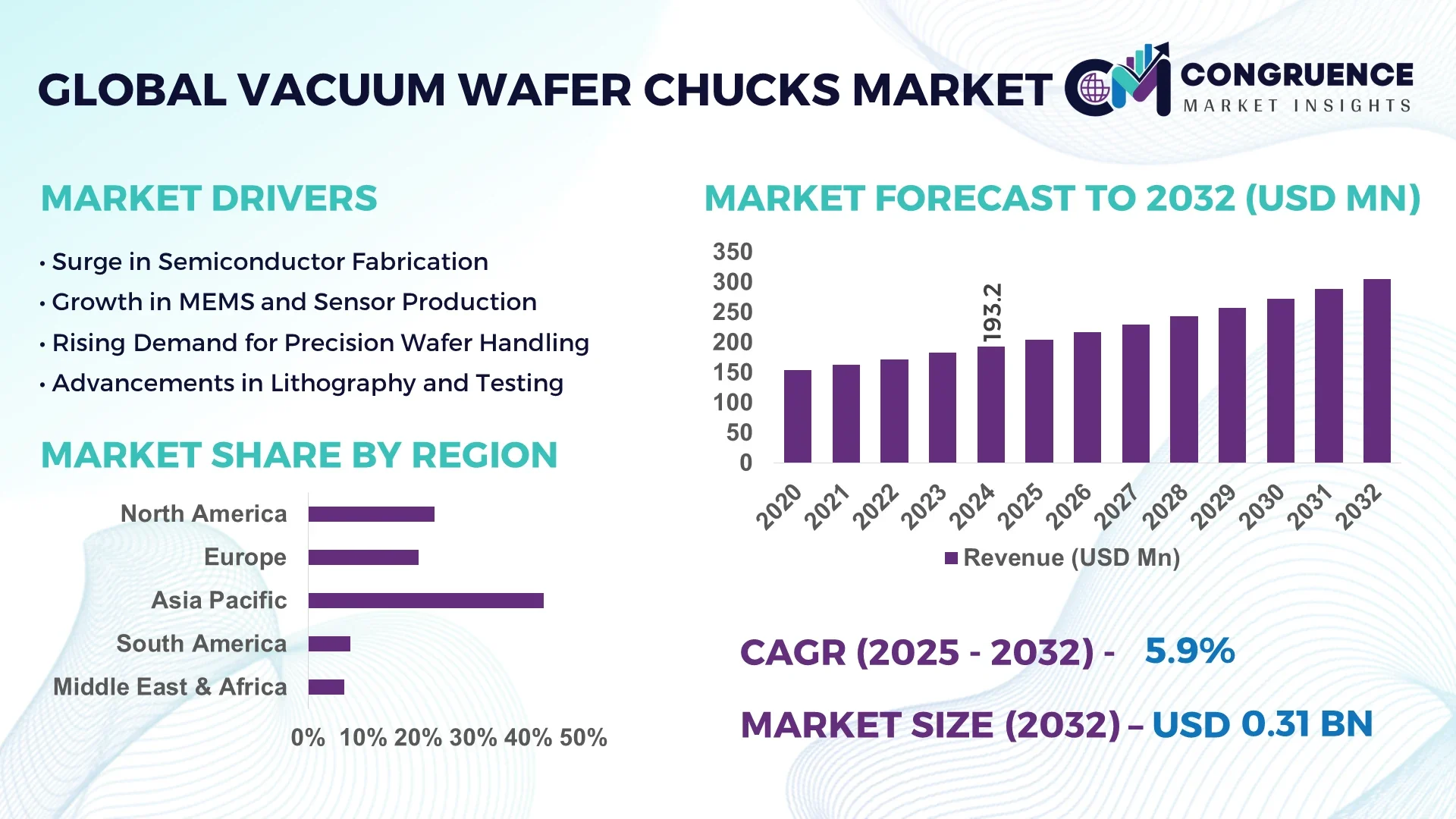
The Global Vacuum Wafer Chucks Market was valued at USD 193.16 Million in 2024 and is anticipated to reach a value of USD 305.55 Million by 2032 expanding at a CAGR of 5.9% between 2025 and 2032.
Japan maintains the largest production capacity in the Vacuum Wafer Chucks market with consistent investments in advanced semiconductor manufacturing technologies, significant high-precision equipment deployment across fabrication facilities, and the rapid integration of robotics into wafer handling processes.
The Vacuum Wafer Chucks Market is expanding rapidly due to increased demand across semiconductor manufacturing, microelectronics, MEMS fabrication, and advanced packaging industries. Key sectors such as 300mm wafer fabrication and high-frequency device manufacturing are driving adoption, with OEMs enhancing product lines to accommodate ultra-thin wafer processing and high-speed automated transfer applications. Technological innovations including non-contact clamping, precision vacuum control, and ceramic-based lightweight chuck structures are enabling advanced wafer handling at lower defect rates. Regulatory frameworks supporting semiconductor expansion and cleanroom standard upgrades are positively impacting procurement in Asia-Pacific, North America, and Europe. The market is also witnessing growing interest in dry vacuum pump integrations and modular chuck platforms to enhance throughput. Emerging trends indicate a shift towards AI-integrated vacuum wafer chuck systems to improve operational efficiency and precision in semiconductor facilities.
Artificial Intelligence is revolutionizing the Vacuum Wafer Chucks Market by driving advanced automation and predictive maintenance in wafer handling systems across semiconductor fabrication lines. AI algorithms integrated into vacuum wafer chuck control systems enable real-time monitoring of clamping force, temperature distribution, and vibration levels, ensuring ultra-precise wafer positioning while minimizing the risk of breakage during high-speed transfer. In smart fabs, AI-powered data analytics support condition-based maintenance of Vacuum Wafer Chucks, reducing downtime by automatically detecting micro-leaks or vacuum inconsistencies before they escalate into operational failures.
AI is also optimizing the Vacuum Wafer Chucks Market by enabling process parameter tuning based on in-situ sensor feedback, which improves wafer flatness and reduces edge warp issues in advanced node manufacturing. The adoption of AI-driven robotics in wafer loading and unloading is enhancing throughput in high-volume production environments, reducing cycle times, and minimizing human intervention to maintain cleanroom integrity. Moreover, machine learning models are being applied to vacuum system diagnostics within Vacuum Wafer Chucks Market setups to predict component fatigue and optimize energy consumption, aligning operational practices with environmental sustainability goals while maintaining ultra-clean process environments. AI’s role in the Vacuum Wafer Chucks Market extends to smart calibration systems, which enable faster changeovers in wafer sizes and thicknesses, supporting dynamic production requirements in the semiconductor industry. These advancements are shaping a future-ready Vacuum Wafer Chucks Market aligned with Industry 4.0 standards.
“In 2024, a leading Japanese semiconductor equipment manufacturer integrated an AI-powered vacuum leakage detection system into its Vacuum Wafer Chucks, which enabled a 40% reduction in unplanned downtime across its pilot fabrication lines by providing real-time diagnostics and predictive alerts, enhancing wafer handling stability in sub-5nm process nodes.”
The Vacuum Wafer Chucks Market is experiencing steady expansion driven by the continuous rise in semiconductor device miniaturization, increased 300mm wafer adoption, and advancements in MEMS and advanced packaging processes. Demand for high-precision wafer handling solutions with minimal particle generation and enhanced thermal control is shaping purchasing decisions across fabrication facilities. The market is witnessing increased integration of automation and smart control systems into vacuum wafer chuck solutions, supporting defect reduction and improving overall operational throughput in semiconductor manufacturing environments. Growth in the electronics and IoT sectors has further fueled demand for reliable wafer handling, while regulatory advancements toward energy-efficient and cleanroom-compliant systems are encouraging investments in modern vacuum wafer chucks. Increasing regional semiconductor investments, particularly in Asia-Pacific and North America, along with supply chain advancements, are also contributing to the evolving Vacuum Wafer Chucks Market landscape.
The demand for vacuum wafer chucks is significantly driven by the rapid expansion of advanced node semiconductor manufacturing across global fabrication plants. As semiconductor manufacturers transition to sub-10nm and sub-5nm process nodes, precise wafer handling with minimal vibration and enhanced flatness control is essential to ensure high yield rates during lithography and etching processes. Vacuum wafer chucks with improved thermal conductivity and non-contact clamping systems are being integrated into advanced EUV lithography setups and thin wafer handling processes, meeting the stringent requirements of advanced semiconductor manufacturing. This expansion across advanced semiconductor nodes is encouraging OEMs and fabrication facilities to invest in technologically advanced vacuum wafer chucks to maintain competitive production capabilities while reducing defect rates and downtime during high-volume operations.
High initial capital investment and maintenance requirements act as a restraint in the Vacuum Wafer Chucks Market, particularly for small to mid-sized semiconductor fabs and MEMS manufacturers. Advanced vacuum wafer chuck systems require precise engineering with specialized materials, high-tolerance machining, and the integration of sophisticated vacuum control mechanisms, leading to elevated procurement costs. Additionally, maintaining optimal vacuum conditions, calibrating vacuum sensors, and ensuring consistent clamping force necessitate periodic maintenance and skilled technical oversight, adding to operational costs. The necessity to operate within strict cleanroom conditions further escalates these maintenance demands, often delaying purchase decisions and limiting adoption for facilities operating under constrained capital budgets within the Vacuum Wafer Chucks Market.
The integration of AI and smart diagnostics into vacuum wafer chuck systems presents a substantial opportunity in the Vacuum Wafer Chucks Market. AI-powered condition monitoring and predictive maintenance functionalities can significantly reduce unplanned downtime while enhancing wafer handling stability in high-precision semiconductor operations. Smart diagnostics can detect micro-leaks, vacuum inconsistencies, and abnormal vibration patterns, enabling early intervention and reducing potential wafer breakage or quality issues during transfer and processing. Additionally, the capability of AI to optimize clamping parameters dynamically based on real-time process data supports energy-efficient operations and improved process throughput. As semiconductor manufacturing facilities worldwide adopt Industry 4.0 practices, the implementation of AI-enhanced vacuum wafer chuck solutions is poised to create new avenues for growth within the Vacuum Wafer Chucks Market.
Meeting stringent cleanroom and contamination control standards poses a significant challenge within the Vacuum Wafer Chucks Market. As semiconductor devices continue to scale down to advanced nodes, even microscopic contaminants can lead to costly defects and yield losses, making contamination control a critical concern for manufacturers. Vacuum wafer chucks must maintain ultra-clean surfaces while providing secure and stable wafer clamping under varying operational conditions, demanding highly engineered designs and advanced filtration systems within the vacuum environment. The complexity of maintaining these conditions during high-volume production increases operational challenges, requiring frequent cleanroom certification and system recalibration, which can interrupt workflow and add to operational expenditures. This challenge necessitates ongoing technological refinement and process innovation in the Vacuum Wafer Chucks Market to meet evolving contamination control demands in semiconductor manufacturing environments.
• Advanced Thin Wafer Handling Innovations: Manufacturers are developing vacuum wafer chucks with enhanced thermal conductivity and lower clamping force specifically designed for handling ultra-thin wafers used in advanced logic and memory applications. These advanced thin wafer handling systems reduce wafer breakage and edge chipping during high-speed processing and are seeing increased deployment in facilities transitioning to sub-5nm nodes.
• AI-Integrated Predictive Maintenance: The Vacuum Wafer Chucks Market is witnessing a clear trend toward AI-based predictive maintenance integration within vacuum chuck systems. Facilities using smart diagnostics have reported a measurable reduction in unplanned downtime, as these systems detect micro-leaks and vibration anomalies, allowing maintenance teams to perform timely interventions while maintaining wafer handling stability in semiconductor production.
• Adoption of Ceramic and Hybrid Material Chucks: There is a notable shift toward ceramic and hybrid material vacuum wafer chucks for their superior thermal stability, chemical resistance, and low particle generation. This trend is especially evident in advanced packaging and MEMS fabrication lines where consistent wafer flatness is critical to maintaining device yield and process integrity.
• Regional Capacity Expansions in Asia-Pacific: Asia-Pacific continues to lead in expanding vacuum wafer chuck capacity due to growing semiconductor investments in countries like Japan, Taiwan, and South Korea. Facilities are upgrading their wafer handling systems with advanced vacuum chuck technologies to support increasing demand in memory, logic, and sensor manufacturing, reinforcing regional equipment procurement trends.
The Vacuum Wafer Chucks Market is segmented by type, application, and end-user insights, each reflecting evolving demand dynamics driven by technological advancements in semiconductor manufacturing. By type, the market includes electrostatic chucks, mechanical chucks, and hybrid chucks, with each addressing specific wafer handling and process needs in semiconductor production. In terms of application, the market serves critical functions in lithography, etching, wafer cleaning, and metrology, where precision handling under vacuum conditions is essential to ensure yield and device performance. End-user segmentation highlights semiconductor foundries, integrated device manufacturers, and research laboratories as the primary users of vacuum wafer chucks, driven by high-volume production requirements and precision R&D needs in advanced node development. This segmentation provides clarity for stakeholders evaluating opportunities across the Vacuum Wafer Chucks Market landscape.
Vacuum wafer chucks are segmented into electrostatic chucks, mechanical chucks, and hybrid chucks, each serving unique semiconductor processing requirements. Electrostatic chucks currently lead due to their superior wafer flatness maintenance and lower particle generation, making them indispensable for advanced lithography and etching processes in semiconductor manufacturing. Mechanical chucks continue to serve legacy processes and specific high-temperature applications requiring robust clamping mechanisms during wafer handling. The fastest-growing type is the hybrid vacuum wafer chuck, which combines mechanical and electrostatic principles to enhance thermal management and wafer stability, supporting the increased demand for processing thin and ultra-thin wafers in advanced node fabrication. Hybrid chucks are seeing adoption across leading-edge semiconductor foundries aiming to enhance production throughput while reducing wafer breakage, aligning with global trends toward high-yield manufacturing. This diversified type segmentation ensures that manufacturers can address varying technical demands within wafer processing environments.
The Vacuum Wafer Chucks Market serves lithography, etching, wafer cleaning, metrology, and wafer inspection applications within semiconductor manufacturing. Lithography remains the leading application, with high demand for precise wafer positioning and flatness during critical exposure processes, supporting the development of sub-5nm and advanced node devices. Etching applications are gaining traction with the increasing complexity of semiconductor device structures, requiring stable and vibration-free wafer handling during plasma etching and deep trench formation processes. The fastest-growing application segment is wafer cleaning, as contamination control becomes critical for maintaining high yield rates, especially in advanced packaging and 3D NAND fabrication lines. Metrology and wafer inspection applications continue to use vacuum wafer chucks for stable positioning during measurement and defect inspection processes, ensuring accurate process control across semiconductor fabs. These application areas collectively define the operational breadth of the Vacuum Wafer Chucks Market in the semiconductor sector.
End-user segments in the Vacuum Wafer Chucks Market include semiconductor foundries, integrated device manufacturers, research laboratories, and equipment OEMs. Semiconductor foundries lead as the primary end-users due to their high-volume wafer processing needs in logic and memory device production, requiring advanced vacuum wafer chuck systems for maintaining precision and yield in demanding manufacturing environments. Integrated device manufacturers are the fastest-growing end-user segment, driven by their ongoing investments in advanced packaging, MEMS production, and the transition to cutting-edge semiconductor nodes that require high-performance wafer handling solutions. Research laboratories and academic semiconductor research centers contribute to the market by using vacuum wafer chucks for development and prototyping of advanced semiconductor processes, supporting innovation and testing of new wafer handling methodologies. Equipment OEMs, while a smaller segment, procure vacuum wafer chucks for integration into turnkey semiconductor manufacturing systems, ensuring compatibility and process optimization for customers. This segmentation highlights how diverse end-user needs shape purchasing trends within the Vacuum Wafer Chucks Market.
Asia-Pacific accounted for the largest market share at 42.8% in 2024 however, North America is expected to register the fastest growth, expanding at a CAGR of 6.7% between 2025 and 2032.

The Vacuum Wafer Chucks Market in Japan benefits from advanced semiconductor manufacturing infrastructure, with high-volume production in wafer handling systems for 300mm and thin wafer applications. The market also sees a consistent demand surge in China due to strong investments in semiconductor fabs and local production of advanced electronic components, including logic and memory chips. Regulatory support for domestic semiconductor capacity expansion, combined with increased adoption of automated vacuum wafer chuck systems to meet advanced packaging and MEMS needs, is strengthening regional consumption patterns. Additionally, the market is witnessing rising technological collaborations in Taiwan and South Korea to integrate AI diagnostics and thin wafer handling within vacuum wafer chuck systems, reinforcing Asia-Pacific’s position in driving global market advancements.
Precision Handling Technologies Drive Market Expansion
North America holds a 22.8% volume share in the Vacuum Wafer Chucks Market, driven by robust semiconductor production for logic devices, advanced sensors, and automotive electronics. Key industries such as aerospace, defense, and consumer electronics are fueling demand for high-precision wafer handling systems that maintain low particle generation and stable wafer positioning during advanced lithography and etching processes. Notable regulatory changes, including incentives under the CHIPS and Science Act, have accelerated investments in semiconductor fabrication capacity, further boosting the adoption of advanced vacuum wafer chuck systems. Technological advancements in the region emphasize the integration of AI-based predictive maintenance and real-time diagnostics in wafer handling to reduce downtime and improve operational throughput in semiconductor facilities.
Adoption of Clean Manufacturing Processes in Semiconductor Production
Holding a 17.5% market share, Europe’s Vacuum Wafer Chucks Market is supported by key markets such as Germany, the UK, and France, where semiconductor and advanced electronics manufacturing remain critical growth pillars. The European Union’s sustainability initiatives and support for local semiconductor production through strategic funding have contributed to the increased adoption of precision vacuum wafer chucks within advanced packaging and MEMS production lines. Regulatory frameworks under REACH and RoHS are encouraging clean manufacturing and process optimization across fabrication plants, leading to higher investments in vacuum wafer chuck systems that align with environmental and cleanroom standards. The region is actively adopting hybrid material chucks and AI-based control systems for wafer handling processes.
Growing Investments in Advanced Semiconductor Manufacturing Infrastructure
Asia-Pacific leads global consumption with over 42.6% of the volume share in the Vacuum Wafer Chucks Market, with China, Japan, South Korea, and Taiwan being the top-consuming countries. The region benefits from a strong semiconductor manufacturing base with expanding advanced node fabrication, thin wafer processing, and high-volume MEMS production. Investments in upgrading semiconductor manufacturing infrastructure to meet domestic and export demand for logic and memory devices have increased procurement of advanced vacuum wafer chuck systems across major fabs. Technological trends include integrating smart diagnostics, hybrid chucks, and low-temperature processing within wafer handling systems, reflecting the region’s continuous focus on technological upgrades and innovation hubs.
Rising Demand from Electronics and Renewable Energy Sectors
The Vacuum Wafer Chucks Market in South America, led by Brazil and Argentina, is gaining traction, with Brazil holding a 3.2% market share. Growth is supported by increasing investments in the electronics assembly and renewable energy sectors, which require precision wafer handling for sensor and microelectronics manufacturing. Government incentives for domestic electronics production and trade policies promoting advanced technology imports are improving access to modern wafer handling solutions across regional facilities. Additionally, the shift towards clean energy technologies has increased the need for advanced semiconductor components, indirectly driving demand for vacuum wafer chucks to support local semiconductor assembly and testing operations.
Emerging Semiconductor Hubs and Diversification Initiatives
The Middle East & Africa Vacuum Wafer Chucks Market is witnessing steady demand from emerging semiconductor hubs in the UAE and South Africa, with UAE driving regional growth. Regional demand is supported by diversification initiatives targeting technology manufacturing and advanced electronics assembly in line with economic vision plans. The market benefits from the adoption of technological modernization strategies across cleanroom environments, with facilities integrating advanced vacuum wafer chuck systems to support local semiconductor packaging and sensor manufacturing. Local regulations and trade partnerships are encouraging investments in advanced manufacturing, further facilitating demand for precision wafer handling equipment across emerging regional semiconductor ecosystems.
Japan – 34.2% market share
High production capacity and advanced semiconductor manufacturing infrastructure in wafer processing facilities drive Japan’s lead in the Vacuum Wafer Chucks Market.
China – 28.9% market share
Strong end-user demand for advanced electronics and aggressive domestic investments in semiconductor fabs support China’s position in the Vacuum Wafer Chucks Market.
The Vacuum Wafer Chucks market features over 35 active competitors globally, with strong positioning by Japanese, South Korean, and US-based manufacturers leading precision wafer handling solutions for semiconductor fabs. Competitive dynamics are shaped by continuous innovation in electrostatic and hybrid vacuum wafer chucks, with companies focusing on non-contact clamping, thin wafer handling, and AI-integrated predictive maintenance technologies to meet the high precision requirements of advanced node manufacturing. Strategic initiatives in the market include collaborations with semiconductor OEMs for system integration, partnerships with automation solution providers, and regional expansions in Asia-Pacific to address growing semiconductor capacity. Recent product launches have introduced lightweight ceramic chucks and advanced control systems that enhance flatness and thermal management during high-speed wafer processing. Companies are investing in in-house R&D to develop low-vibration and cleanroom-compatible chuck systems that align with advanced packaging and MEMS manufacturing trends, reinforcing competitive positions while addressing the evolving demands of semiconductor production environments globally.
TOTO Ltd.
SUSS MicroTec SE
DISCO Corporation
Lam Research Corporation
SHINKO Electric Industries Co., Ltd.
EBM-Papst Group
Tokyo Electron Limited
Kitano Seiki Co., Ltd.
AMAT Precision Materials Inc.
Logitech Ltd.
The Vacuum Wafer Chucks Market is witnessing significant technological advancements focused on enhancing wafer handling precision, reducing contamination risks, and improving process flexibility in advanced semiconductor manufacturing environments. One key development is the adoption of advanced electrostatic chuck designs that enable stable clamping of thin and ultra-thin wafers during high-speed lithography and etching without inducing stress or warping, maintaining wafer flatness within 1-2 µm tolerance. Ceramic and hybrid material chucks are gaining traction for their thermal stability and low particle generation, essential for sub-5nm and EUV lithography applications.
Technologies integrating AI-based predictive maintenance and smart vacuum diagnostics are being implemented to monitor clamping forces, detect micro-leaks, and optimize wafer handling parameters in real time, reducing unplanned downtime in fabs. Multi-zone temperature control within vacuum wafer chucks is another innovation supporting advanced packaging, where different die sizes and wafer thicknesses require precise thermal management during bonding and dicing. Dry vacuum pump integration within wafer chuck systems is reducing contamination while ensuring high vacuum integrity, supporting cleanroom compliance.
Emerging trends include contactless clamping systems for fragile wafers used in MEMS and power device manufacturing, providing damage-free handling during processing. Additionally, manufacturers are adopting modular vacuum wafer chuck designs compatible with various wafer sizes, allowing flexible adaptation to shifting semiconductor production needs and advanced device architectures.
• In March 2023, Lam Research introduced a new advanced electrostatic vacuum wafer chuck system designed for EUV lithography, capable of handling ultra-thin wafers with a flatness tolerance of ±1.5 µm, targeting high-volume semiconductor fabs upgrading to sub-5nm node production lines.
• In August 2023, Tokyo Electron launched a vacuum wafer chuck platform integrated with smart AI diagnostics capable of real-time leak detection and clamping force adjustments, reducing unplanned downtime in semiconductor fabs by 28% during the first six months of pilot deployment.
• In February 2024, SUSS MicroTec unveiled a hybrid ceramic vacuum wafer chuck for advanced MEMS processing, providing enhanced thermal uniformity and low particle generation, with adoption in two major Asian semiconductor foundries for thin wafer handling and microfabrication.
• In May 2024, DISCO Corporation developed a modular vacuum wafer chuck system compatible with 150mm to 300mm wafers, integrating multi-zone heating capabilities to support advanced packaging and power device fabrication, enhancing processing flexibility for semiconductor manufacturers.
The Vacuum Wafer Chucks Market Report covers a comprehensive analysis of current and emerging market dynamics, technological innovations, and competitive strategies shaping the global landscape for precision wafer handling in semiconductor manufacturing. The report examines electrostatic, mechanical, and hybrid vacuum wafer chuck technologies with in-depth insights into their application across lithography, etching, wafer cleaning, metrology, and advanced packaging processes. Geographically, the report covers North America, Europe, Asia-Pacific, South America, and the Middle East & Africa, focusing on consumption patterns, technological adoption rates, and manufacturing infrastructure influencing market demand in each region. The analysis includes detailed evaluations of semiconductor foundries, integrated device manufacturers, research laboratories, and equipment OEMs as key end-user segments.
The report also assesses the impact of technological trends such as AI-integrated predictive maintenance, smart diagnostics, multi-zone thermal control, and advanced material adoption within vacuum wafer chuck systems on operational efficiencies and manufacturing yield improvements. It highlights niche opportunities in MEMS and power device fabrication requiring advanced wafer handling solutions, aligning with the increasing demand for thin and ultra-thin wafer processing capabilities. Additionally, the report evaluates regional regulatory frameworks, environmental compliance standards, and government initiatives supporting semiconductor manufacturing expansion, providing actionable insights for stakeholders seeking to understand the evolving competitive landscape and technological positioning within the Vacuum Wafer Chucks Market.
| Report Attribute/Metric | Report Details |
|---|---|
|
Market Revenue in 2024 |
USD 193.16 Million |
|
Market Revenue in 2032 |
USD 305.55 Million |
|
CAGR (2025 - 2032) |
5.9% |
|
Base Year |
2024 |
|
Forecast Period |
2025 - 2032 |
|
Historic Period |
2020 - 2024 |
|
Segments Covered |
By Types
By Application
By End-User
|
|
Key Report Deliverable |
Revenue Forecast, Growth Trends, Market Dynamics, Segmental Overview, Regional and Country-wise Analysis, Competition Landscape |
|
Region Covered |
North America, Europe, Asia-Pacific, South America, Middle East, Africa |
|
Key Players Analyzed |
TOTO Ltd., SUSS MicroTec SE, DISCO Corporation, Lam Research Corporation, SHINKO Electric Industries Co., Ltd., EBM-Papst Group, Tokyo Electron Limited, Kitano Seiki Co., Ltd., AMAT Precision Materials Inc., Logitech Ltd. |
|
Customization & Pricing |
Available on Request (10% Customization is Free) |


