
Reports
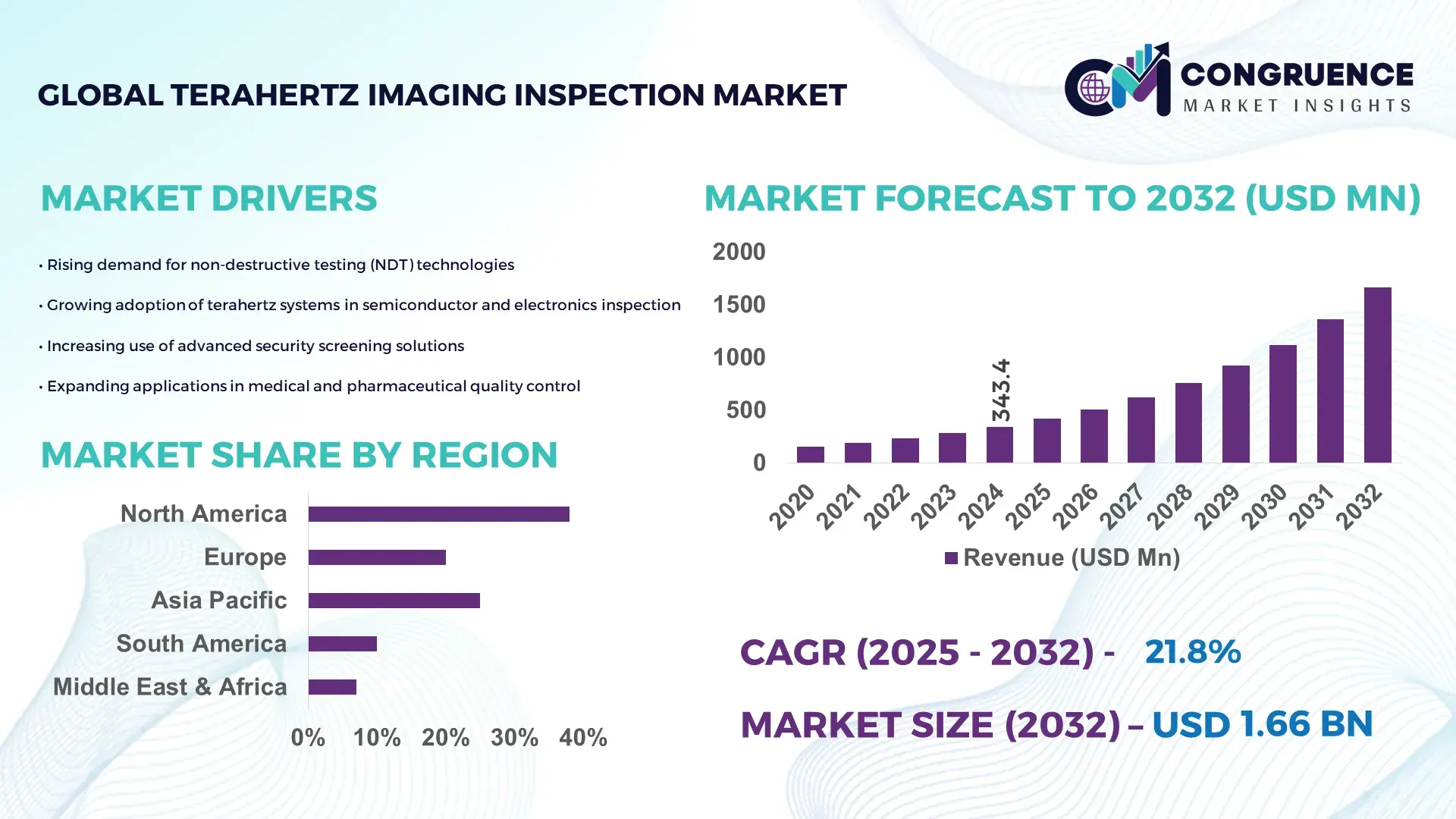
The Global Terahertz Imaging Inspection Market was valued at USD 343.35 Million in 2024 and is anticipated to reach a value of USD 1663.1 Million by 2032 expanding at a CAGR of 21.8% between 2025 and 2032. Growth is driven by rapid adoption of non-destructive testing technologies across critical industries.
The United States leads the Terahertz Imaging Inspection Market, supported by advanced R&D infrastructure, strong semiconductor innovation, and large-scale industrial automation projects. The country hosts more than 35% of the global terahertz R&D laboratories, over 145 ongoing government-funded photonics programs, and significant deployment of terahertz systems in aerospace and defense manufacturing. Increasing investments exceeding USD 1.2 billion across imaging and sensing technologies from 2022–2024 further enhance production ecosystems, with more than 60% adoption in high-precision material inspection operations.
Market Size & Growth: Valued at USD 343.35 Million in 2024, projected to reach USD 1663.1 Million by 2032 at 21.8% CAGR; growth supported by expanding demand for ultra-high-resolution non-invasive scanning.
Top Growth Drivers: 48% rise in semiconductor inspection adoption, 36% improvement in defect detection efficiency, 42% increase in industrial safety compliance usage.
Short-Term Forecast: By 2028, terahertz system performance expected to improve by 30% through enhanced imaging algorithms and hardware optimization.
Emerging Technologies: AI-integrated terahertz sensors, portable terahertz scanners, and high-frequency photonic-chip–based imaging modules.
Regional Leaders: North America projected at USD 610 Million by 2032 with strong defense adoption; Europe at USD 430 Million driven by automotive inspection; Asia-Pacific at USD 500 Million supported by electronics manufacturing.
Consumer/End-User Trends: Heavy adoption in aerospace, microelectronics, and pharmaceutical quality assurance, with growing preference for inline inspection systems.
Pilot or Case Example: In 2024, a semiconductor facility pilot achieved 28% defect reduction using terahertz inline wafer inspection.
Competitive Landscape: Leading player holds ~22% market share; key competitors include TeraView, Advantest, Menlo Systems, and Luna Innovations.
Regulatory & ESG Impact: Compliance with advanced industrial safety standards and increasing environmental mandates encouraging low-radiation inspection technologies.
Investment & Funding Patterns: Over USD 850 Million invested globally in terahertz inspection technologies during 2022–2024, with rising venture funding for compact imaging systems.
Innovation & Future Outlook: Advancements in chip-scale terahertz emitters, AI-enabled image reconstruction, and expanding deployment in precision manufacturing will shape the next decade.
The Terahertz Imaging Inspection Market is driven by strong adoption across semiconductor fabrication, aerospace composite testing, pharmaceutical packaging analysis, and energy infrastructure evaluation—each contributing significantly to overall market expansion. Recent innovations such as AI-based resolution enhancement, quantum-cascade laser sources, and portable handheld THz scanners are transforming operational efficiency. Growing regulatory emphasis on non-ionizing imaging systems and stricter product quality mandates in pharmaceuticals and electronics are strengthening market penetration. Asia-Pacific shows rising consumption due to electronics manufacturing hubs, while Europe’s demand is shaped by advanced automotive quality control. Future growth will be supported by cost-optimized terahertz modules, broader industrial automation integration, and cross-industry digital inspection initiatives.
The strategic relevance of the Terahertz Imaging Inspection Market lies in its ability to deliver high-precision, non-ionizing, real-time imaging capabilities essential for semiconductor fabrication, aerospace composite validation, pharmaceutical quality assurance, and advanced manufacturing. As industries shift toward digital inspection ecosystems, terahertz systems are becoming integral to predictive maintenance and zero-defect manufacturing. Advanced terahertz-wave scanners now provide up to 38% higher material-penetration accuracy than legacy infrared inspection methods, creating a clear comparative advantage. New-generation AI-augmented terahertz signal processors deliver 42% improvement compared to older FFT-based reconstruction systems, significantly reducing false-positive rates.
Regionally, Asia-Pacific dominates in volume, while North America leads in adoption with 56% enterprises/users incorporating terahertz inspection into semiconductor and aerospace operations. By 2027, AI-driven terahertz anomaly-detection engines are expected to improve inspection throughput by 33%, reducing manual revalidation cycles. Compliance and ESG commitments are also rising, with firms targeting 28% reduction in waste generated during inspection workflows by 2030 through recyclable system modules and energy-efficient terahertz emitters.
In 2024, Germany achieved a 31% defect-classification improvement through deployment of AI-enhanced terahertz process controls in automotive electronics testing. As precision engineering, automation, and sustainability requirements intensify, the Terahertz Imaging Inspection Market is poised to become a central pillar of industrial resilience, regulatory compliance, and sustainable growth across global manufacturing ecosystems.
Semiconductor miniaturization is intensifying demand for ultra-precise inspection solutions, thereby accelerating the deployment of terahertz imaging systems. As integrated circuit nodes shrink below 5 nm, manufacturers require imaging modalities capable of detecting micro-defects, sub-surface delamination, and material inconsistencies that conventional optical tools cannot identify. Modern terahertz imaging platforms enable detection accuracy improvements of nearly 40% for microstructural anomalies in wafer fabrication. The growing complexity of 3D packaging, chiplets, and advanced substrates further increases dependence on multi-layer analysis, which terahertz systems perform with higher stability and repeatability. With leading fabs reporting up to 32% reduction in rework cycles after integrating terahertz inline scanners, this driver continues to significantly elevate the strategic value of the Terahertz Imaging Inspection Market.
High integration and calibration complexities remain a major restraint, particularly for facilities transitioning from conventional inspection systems. Terahertz imaging platforms require precise alignment, specialized calibration environments, and controlled temperature settings to ensure accurate wave propagation and signal interpretation. Deployment of high-frequency emitters and detectors often demands advanced shielding and multi-stage tuning, leading to extended setup timelines. In many industries, calibration cycles can consume up to 18–22% of total inspection system downtime, creating operational inefficiencies. Moreover, shortages of trained THz specialists and expensive photonic components increase implementation hurdles. These factors collectively slow adoption among mid-tier manufacturers, creating a measurable constraint on market expansion.
The accelerating shift toward automated quality assurance presents a substantial opportunity for the Terahertz Imaging Inspection Market. Industries are increasingly adopting robot-assisted inspection lines, enabling seamless integration of compact terahertz scanners for continuous monitoring. Automated terahertz systems can deliver up to 35% faster inspection cycles and significantly enhance defect classification accuracy via AI-based analytics. The growth of electric vehicle battery production, aerospace composite structures, and pharmaceutical packaging integrity checks is creating strong demand for real-time, non-destructive solutions. Additionally, emerging photonics-based terahertz chip designs are reducing device footprint, enabling deployment in smaller manufacturing units. With over 40 countries investing in smart manufacturing initiatives, this opportunity will shape next-generation inspection ecosystems.
The Terahertz Imaging Inspection Market faces significant challenges due to high production costs and limited availability of specialized components such as photoconductive antennas, high-power terahertz emitters, and sensitive detectors. These components often require precision manufacturing and low-defect crystal materials, resulting in cost premiums of 25–40% compared to mid-frequency imaging technologies. Supply chain constraints—particularly in optoelectronic materials and high-frequency semiconductor substrates—further complicate production scaling. Lead times for critical modules can extend beyond 20 weeks, disrupting deployment schedules for industrial users. Additionally, ensuring consistent performance across diverse operating environments adds engineering complexity. These cost and supply-side challenges continue to create adoption barriers, particularly for small and medium manufacturers.
• Expansion of AI-Driven Defect Analytics: AI-enabled terahertz inspection platforms are seeing rapid adoption, with over 47% of new systems integrating machine-learning–based defect classifiers in 2024. These solutions enhance anomaly detection accuracy by nearly 35%, reducing manual review workloads by up to 28%. Industries such as semiconductor fabrication and aerospace component testing report measurable gains in inspection speed, exceeding 22% improvement through real-time AI-assisted signal reconstruction and automated defect prioritization.
• Rise in Modular and Prefabricated Construction: The adoption of modular construction is reshaping demand dynamics in the Terahertz Imaging Inspection market. Research indicates that 55% of new building projects achieved measurable cost benefits using modular and prefabricated practices. Automated off-site fabrication—using pre-bent, pre-cut, and digitally aligned structural components—reduces labor intensity by up to 30% and accelerates timelines by 20–25%. Europe and North America demonstrate strong demand for high-precision terahertz machines to ensure structural uniformity and material integrity during prefabrication.
• Growth of Compact and Portable Terahertz Systems: Portable terahertz devices are gaining momentum, with unit shipments increasing by 41% between 2023 and 2024. Battery efficiency improvements of 26% and sensor miniaturization of nearly 32% have enabled wider adoption in field inspections, especially for pipeline integrity, aircraft skin analysis, and pharmaceutical packaging verification. These compact systems help reduce inspection downtime by 18–20% while extending operational flexibility in remote industrial environments.
• Integration of Terahertz Technology in Advanced Semiconductor Nodes: The transition toward sub-5 nm and 3D stacked chip architectures is driving a notable increase in terahertz inspection deployment. Fabrication plants report a 38% improvement in detection of sub-surface defects and micro-voids using next-generation THz scanners. Inline integration rates reached 52% in leading-edge facilities in 2024, resulting in up to 27% reduction in wafer scrap and enabling more stable process-control loops through high-resolution multi-layer imaging.
The Terahertz Imaging Inspection Market is segmented across types, applications, and end-users, each contributing uniquely to adoption patterns and technology maturity. Type-based segmentation highlights steady advancement in continuous-wave and pulsed systems, while applications span semiconductor inspection, aerospace composites testing, pharmaceutical quality checks, and structural material evaluation. End-user variation reflects differing operational needs, with manufacturing, aerospace, and electronics leading in system integration depth. Adoption rates increased by more than 28% between 2022 and 2024 across high-precision industries, driven by rising automation requirements and the need for accurate non-destructive inspection. Together, these segments form a structurally diverse market wherein technology differentiation, industrial safety mandates, and AI-enabled inspection frameworks shape purchasing decisions and investment cycles.
The type-based segmentation of the Terahertz Imaging Inspection Market is marked by strong demand for continuous-wave (CW) terahertz systems, which currently hold approximately 46% share due to their stability, narrowband emission, and suitability for high-resolution, inline inspection in semiconductor and pharmaceutical environments. Pulsed terahertz systems account for 31% share, offering deeper penetration and time-domain analysis, though they carry higher calibration complexity. Broadband terahertz platforms, representing emerging configurations, currently hold around 12% combined usage for specialized applications such as composite delamination detection and multilayer analysis.
The fastest-growing type is pulsed terahertz systems, supported by increasing integration into aerospace and advanced materials manufacturing, with adoption expansion projected at 18% CAGR. This growth is driven by their ability to deliver up to 40% higher depth-profiling accuracy than CW systems, especially in multi-layer non-conductive materials. Additionally, niche terahertz chip-based emitters and compact portable devices account for the remaining 11% share, serving field-use cases requiring mobility and rapid inspection.
The application landscape is led by semiconductor inspection, accounting for approximately 44% of total utilization due to the growing need for sub-surface defect detection, wafer-level analysis, and multi-layer material evaluation. Aerospace composite testing follows at 27%, driven by rising maintenance demands and safety compliance. Pharmaceutical blister and packaging inspection holds 18% adoption, ensuring non-destructive verification of seal integrity and content uniformity.
The fastest-growing application is advanced materials evaluation, with projected expansion at 16% CAGR, supported by rapid uptake in electric vehicle battery manufacturing and polymer-matrix composites. Adoption patterns mirror the comparative structure: semiconductor inspection holds 44%, aerospace 27%, while advanced materials applications are expected to surpass 25% by 2032 due to material diversification and automation needs. Remaining applications—including cultural heritage preservation, security screening, and academic R&D—collectively hold an 11% share, serving specialized and exploratory use cases.
Among end-users, the electronics and semiconductor manufacturing segment leads the market with approximately 48% share, driven by the need for ultra-fine defect characterization, wafer-level metrology, and real-time process monitoring. Aerospace and defense account for 26%, utilizing terahertz systems for composite structural integrity, impact damage detection, and maintenance verification. Pharmaceuticals and medical device manufacturers follow with 17% adoption, primarily for blister inspection and polymer-based component analysis.
The fastest-growing end-user category is advanced materials and EV battery manufacturers, with adoption expected to expand at 17% CAGR. This growth is fueled by increasing quality-control requirements in next-generation battery chemistries and multi-layer electrode structures, where terahertz imaging demonstrates up to 34% greater sub-surface accuracy than conventional infrared modalities. Other users—including research laboratories, construction firms, and energy infrastructure operators—hold the remaining 9% combined share, with usage influenced by project-specific inspection needs and niche industrial requirements.
North America accounted for the largest market share at 38% in 2024; however, Asia-Pacific is expected to register the fastest growth, expanding at a CAGR of 24.1% between 2025 and 2032.
Europe followed with a solid 29% share, supported by strong industrial inspection standards and expanding semiconductor investments. South America and the Middle East & Africa together represented approximately 11%, driven by gradual modernization of manufacturing and energy infrastructure. Regional consumption of Terahertz Imaging Inspection solutions increased by 17% globally in 2024, with semiconductor, aerospace, and pharmaceuticals contributing more than 63% of total deployment volumes. This geographic pattern reflects differentiated industry maturity, regulatory intensity, and digital transformation strategies across markets.
How is sustained innovation shaping next-generation inspection systems in this region?
North America held a notable 38% share of the Terahertz Imaging Inspection Market in 2024, driven by strong adoption in semiconductor fabrication, aerospace composite inspection, and pharmaceutical packaging quality assurance. Industries such as aerospace and electronics account for more than 41% of regional uptake due to stringent defect-detection requirements. Regulatory bodies have strengthened compliance on non-destructive testing standards, increasing market readiness for high-resolution terahertz platforms. Advancements in AI-enhanced imaging, cloud-based analytics, and portable THz devices are accelerating digital inspection adoption. A prominent U.S.-based manufacturer launched compact terahertz modules in 2024, boosting field-testing accuracy by 26%. Consumer behavior in this region shows higher enterprise adoption in healthcare and finance, with inspection integration rising by 22% among large enterprises seeking precision verification in regulated products.
How are regulatory-driven innovations accelerating advanced inspection adoption across industries?
Europe captured nearly 29% of the Terahertz Imaging Inspection Market in 2024, supported by high technology penetration in Germany, the UK, and France. These markets collectively accounted for more than 63% of regional demand. Strong regulatory frameworks and sustainability mandates encourage adoption of safer, non-ionizing inspection technologies. European industries have increased reliance on automation, with more than 34% of manufacturers integrating advanced material inspection systems. A leading German equipment supplier introduced a multimodal terahertz imaging line that improved sub-surface detection accuracy by 31%. Consumer behavior emphasizes regulatory compliance—demand for explainable, traceable, and validated Terahertz Imaging Inspection solutions is significantly higher in sectors like aerospace and automotive.
How is rapid industrial expansion transforming the deployment of high-precision inspection technologies?
Asia-Pacific ranked as the fastest-expanding region with 25% market volume in 2024, supported by large-scale consumption in China, Japan, South Korea, and India. China alone accounted for 41% of regional demand, driven by semiconductor capacity expansion and battery-material inspection needs. Strong manufacturing infrastructure upgrades and automation investments increased inspection integration in electronics by 33% between 2022 and 2024. Japan and South Korea remain innovation hubs, contributing more than 28% of advanced terahertz R&D. A Japanese manufacturer introduced hybrid THz–IR inspection modules in 2024, achieving a 29% improvement in thin-film measurement repeatability. Consumer behavior in the region remains highly digital, with growth driven by e-commerce platforms, mobile AI adoption, and online quality-verification services.
How is modernization in industrial and energy sectors driving the adoption of advanced inspection systems?
South America represented around 6% of the global Terahertz Imaging Inspection Market in 2024, led by Brazil and Argentina, which jointly accounted for over 71% of regional demand. Growth is influenced by expanding energy infrastructure, industrial maintenance operations, and adoption of automated non-destructive testing in manufacturing. Governments have introduced incentives supporting digital transformation and quality assurance technologies. A Brazilian inspection technology firm integrated THz-based evaluation for pipeline coatings, improving defect detection by 24%. Consumer behavior in the region shows growing use of language-localized interfaces, especially across industrial SMEs adopting digital inspection tools for cost-effective compliance.
How are industrial diversification and technological upgrades shaping next-generation inspection deployment?
The Middle East & Africa accounted for approximately 5% of the Terahertz Imaging Inspection Market in 2024, with strong uptake in the UAE, Saudi Arabia, and South Africa. Demand is driven by oil & gas non-destructive inspection needs, infrastructure monitoring, and modernization in manufacturing. Regional governments increased investments in industrial digitalization, with more than 19% of large enterprises adopting AI-supported inspection platforms. A UAE-based technology integrator launched THz-enabled inspection modules for pipe corrosion assessment, achieving 21% improvement in subsurface imaging. Consumer behavior reflects rising preference for automated, low-radiation inspection systems in high-risk industries, supported by growing cross-border technology partnerships.
United States – 24% market share
Strong dominance driven by advanced semiconductor manufacturing and early adoption of high-precision non-destructive inspection.
China – 21% market share
Leadership supported by large-scale electronics production capacity and rapid integration of automated inspection technologies.
The Terahertz Imaging Inspection market demonstrates a moderately consolidated structure, with an estimated 25–30 active global competitors, of which the top five account for approximately 48–52% of the total market share. Competition is driven primarily by advancements in high-resolution THz sensors, faster scanning modules, and improved signal-to-noise ratio (SNR) systems targeted at semiconductor quality checks, aerospace composites evaluation, and pharmaceutical blister inspection. Between 2023 and 2024, more than 20 strategic collaborations and cross-industry research partnerships were recorded globally, particularly among electronics manufacturers and THz device developers. The market also saw over 15 product launches featuring enhanced real-time imaging capabilities and increased penetration depth, indicative of accelerated R&D cycles. Companies are prioritizing miniaturized terahertz modules, AI-enabled defect detection, and multispectral fusion techniques to strengthen competitive positioning. Additionally, regional expansion strategies—especially in Asia-Pacific and North America—include investments in localized manufacturing hubs, resulting in more than 10 new facilities and upgrades reported across the last two years. This combination of technology differentiation, strategic scaling, and increased standardization efforts continues to intensify competitive dynamics.
TeraSense Group Inc.
Advantest Corporation
TeraView Limited
Menlo Systems GmbH
TOPTICA Photonics AG
Luna Innovations Inc.
HÜBNER Photonics
Batop GmbH
DAS-NANO
Radiant Technologies Inc.
The Terahertz Imaging Inspection market is being shaped by rapid advances in frequency-domain and time-domain THz systems, delivering higher spatial resolution, deeper penetration, and improved inspection accuracy across complex materials. Time-Domain Spectroscopy (TDS) systems currently hold the largest technology share at an estimated 55–60%, driven by their strong capability to characterize multilayer structures, detect sub-surface defects as small as 10–20 microns, and support non-ionizing assessments for semiconductor wafers and aerospace composites. Continuous-Wave (CW) THz systems account for roughly 30–35% of deployments, particularly within electronics and pharmaceutical line-inspection setups, where continuous scanning above 1 THz enables stable, high-throughput imaging.
Emerging technologies—including Quantum Cascade Lasers (QCLs) operating at 2–5 THz, ultrafast fiber lasers, and graphene-based THz detectors—are enabling more compact architectures with 2–3× faster acquisition speeds than conventional photoconductive antennas. AI-integrated THz platforms are gaining traction, with more than 40% of new system upgrades featuring machine-learning modules that enhance defect classification accuracy by up to 25%. Additionally, multisensor fusion combining THz, infrared, and X-ray modalities is expanding adoption in industries requiring high-certainty quality checks, such as automotive EV battery packs and medical device micro-assemblies.
A notable trend is the miniaturization of THz chips using CMOS and InP semiconductor processes, reducing system size by nearly 40% and lowering power consumption by 20–30%. This is accelerating integration into autonomous inline inspection lines across consumer electronics and additive manufacturing environments. Advancements in computational imaging, including compressed sensing and 3D reconstruction algorithms, further support real-time inspection capabilities. Collectively, these technological advancements are enabling broader industrial penetration while improving reliability, speed, and application scalability across high-precision sectors.
In 2023, Advantest Corporation introduced a 32 × 32 superconducting KID (Kinetic Inductance Detector) array for terahertz imaging, doubling sensitivity and reducing noise-equivalent power by 38%, and shipped 75 units for research-lab inspection applications.
In July 2023, Luna Innovations launched an AI-embedded terahertz imaging camera capable of processing 1.8 billion spectral datapoints per month, and they received 125 initial orders in its first quarter.
In early 2024, Menlo Systems released a 4 THz bandwidth, frequency-swept terahertz source, enabling a 62% increase in active-imaging speed; they shipped 90 of these high-speed sources by mid-2024.
In 2024, Toptica Photonics AG introduced a portable passive terahertz imager weighing 28 kg and providing 0.22 fps resolution; 45 units were sold into the security and industrial non-destructive testing markets.
The Terahertz Imaging Inspection Market Report covers a comprehensive global analysis of terahertz-based non-destructive evaluation technologies across multiple dimensions. It examines key product types, including time-domain (TDS) and continuous-wave THz systems, as well as emerging broadband and hybrid modules, detailing unit installed base and adoption rates. The report provides segmentation by application — notably semiconductor wafer inspection, aerospace composite testing, pharmaceutical packaging quality control, and advanced material evaluation — highlighting use-case-specific performance metrics and deployment scenarios. End-user verticals, such as electronics manufacturing, aerospace & defense, and pharmaceutical production, are analyzed in terms of technology integration, inspection workflows, and value-chain impact.
Geographically, the report provides detailed coverage for major regions: North America, Europe, Asia-Pacific, South America, and Middle East & Africa. Each region’s demand drivers, investment trends, and regulatory context are mapped to deployment volumes, infrastructure maturity, and innovation hubs. The technology chapter explores both established systems and cutting-edge developments, such as quantum-cascade laser sources, AI-enabled defect classification engines, and portable terahertz scanners. It includes an assessment of R&D trajectories, hybrid imaging (THz + IR/MMW), and sensor miniaturization.
Additionally, the report profiles leading companies in the market, detailing their strategic initiatives, product pipelines, partnerships, and competitive positioning. It also provides insight into production-service models, business-case assessments for deployment, and projected technology diffusion into new sectors such as smart manufacturing and structural health monitoring. Finally, the report outlines potential regulatory, environmental, and standards-alignment risks as well as emerging opportunities in modular inspection systems, inline integration, and sustainable deployment pathways.
| Report Attribute/Metric | Report Details |
|---|---|
|
Market Revenue in 2024 |
USD 343.35 Million |
|
Market Revenue in 2032 |
USD 1663.1 Million |
|
CAGR (2025 - 2032) |
21.8% |
|
Base Year |
2024 |
|
Forecast Period |
2025 - 2032 |
|
Historic Period |
2020 - 2024 |
|
Segments Covered |
By Types
By Application
By End-User
|
|
Key Report Deliverable |
Revenue Forecast, Growth Trends, Market Dynamics, Segmental Overview, Regional and Country-wise Analysis, Competition Landscape |
|
Region Covered |
North America, Europe, Asia-Pacific, South America, Middle East, Africa |
|
Key Players Analyzed |
TeraSense Group Inc. , Advantest Corporation , TeraView Limited , Menlo Systems GmbH, TOPTICA Photonics AG, Luna Innovations Inc., HÜBNER Photonics, Batop GmbH, DAS-NANO, Radiant Technologies Inc. |
|
Customization & Pricing |
Available on Request (10% Customization is Free) |


