
Reports
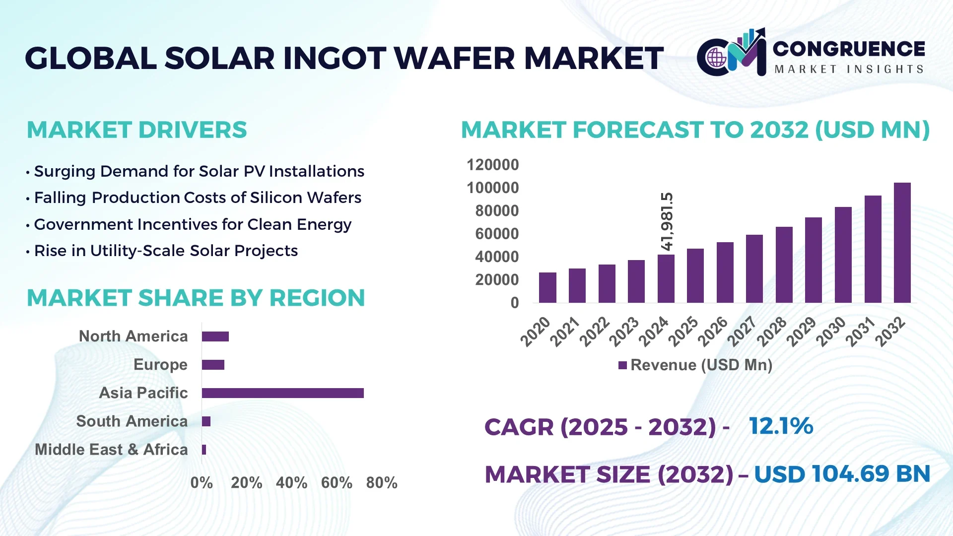
The Global Solar Ingot Wafer Market was valued at USD 41,981.45 Million in 2024 and is anticipated to reach a value of USD 104,689.3 Million by 2032 expanding at a CAGR of 12.1% between 2025 and 2032.
China holds a commanding position in the Solar Ingot Wafer Market with its extensive production capacities, heavy investments in advanced mono-crystalline and polycrystalline ingot pulling lines, cutting-edge wafer slicing facilities, and the integration of AI-enabled quality control in large-scale plants to serve the photovoltaic and energy storage sectors.
The Solar Ingot Wafer Market is witnessing rapid evolution driven by rising solar PV installations, declining module prices, and supportive clean energy policies across major economies. The market benefits from advancements in diamond wire sawing technology and high-efficiency PERC cell-compatible wafer production, enabling thinner wafers while maintaining structural integrity. Emerging markets in Southeast Asia and the Middle East are contributing to demand with increased utility-scale solar projects, while Europe is focusing on building domestic wafer manufacturing to strengthen energy security. Environmental concerns and the push toward carbon neutrality are driving investment in green ingot casting and recycling of silicon kerf loss, while ongoing R&D in heterojunction and TOPCon compatible wafers is setting the stage for the next phase of technological transition within the Solar Ingot Wafer Market.
Artificial Intelligence is playing a transformative role in the Solar Ingot Wafer Market by optimizing production efficiency, reducing material wastage, and enhancing yield rates across manufacturing lines. AI-powered predictive maintenance models are minimizing unplanned downtimes by analyzing vibration, temperature, and power consumption data in ingot pulling and wafer slicing machines. This results in improved operational uptime, reducing costly stoppages in large-scale wafer manufacturing. Machine learning algorithms are enabling precision monitoring of crystal growth parameters, helping manufacturers maintain consistent quality while achieving thinner wafer production aligned with the requirements of high-efficiency solar cells.
In the Solar Ingot Wafer Market, AI-driven quality inspection systems using computer vision are reducing human error and increasing inspection speeds, ensuring defect-free wafers with lower micro-crack rates before cell processing. Additionally, AI is streamlining supply chain management by forecasting demand patterns for wafers across key solar markets, enabling manufacturers to align production with utility-scale project timelines efficiently. The use of digital twins powered by AI is allowing manufacturers to simulate and optimize ingot and wafer production under varying conditions, reducing energy consumption and silicon kerf loss. This integration of AI within the Solar Ingot Wafer Market is accelerating the industry’s move towards high-throughput, low-cost, and sustainable wafer production to meet growing global solar PV deployment targets while enhancing competitiveness for leading players across the supply chain.
"In 2024, a major Chinese solar wafer manufacturer implemented an AI-based wafer defect detection system capable of scanning 8,000 wafers per hour with over 98% accuracy, reducing manual inspection time by 85% and decreasing wafer rejection rates by 12% in its Jiangsu facility."
The Solar Ingot Wafer Market is experiencing robust momentum driven by increased global solar energy installations, technological enhancements in wafer manufacturing, and supportive government policies promoting renewable energy adoption. The market is influenced by the shift from multi-crystalline to mono-crystalline wafers due to higher efficiency requirements for advanced solar modules. Innovations in diamond wire sawing, reduced kerf loss techniques, and the adoption of high-purity silicon are enabling thinner, higher-quality wafers for next-generation solar cells. Additionally, manufacturers in the Solar Ingot Wafer Market are expanding production lines while integrating automation and AI to enhance throughput and maintain consistent wafer quality. The push towards carbon neutrality is further accelerating the demand for sustainable wafer production, while supply chain localization efforts in Europe and North America are shaping regional market dynamics. Increasing investments in utility-scale solar projects in Asia-Pacific and the Middle East are also fueling wafer demand, aligning the Solar Ingot Wafer Market with the global transition towards clean energy.
Technological advancements in wafer production are significantly driving growth in the Solar Ingot Wafer Market. The integration of diamond wire sawing technology has allowed manufacturers to produce ultra-thin wafers while reducing silicon material loss during slicing, which helps lower production costs and enhances yield rates. Developments in mono-crystalline ingot growth, including continuous Czochralski methods, are increasing production speeds while maintaining crystal quality critical for high-efficiency solar modules. Additionally, advancements in heterojunction and TOPCon cell-compatible wafer technology are aligning the Solar Ingot Wafer Market with the next generation of photovoltaic technologies, creating additional demand for high-quality, defect-free wafers. These technological shifts support higher module efficiencies, which are in high demand from utility-scale and residential solar project developers.
Fluctuations in polysilicon supply and prices are posing a restraint in the Solar Ingot Wafer Market. The wafer production process is highly dependent on the availability of high-purity polysilicon, and supply chain disruptions due to trade policies, energy constraints, or production outages can impact wafer manufacturers’ ability to maintain consistent output levels. Price volatility in polysilicon directly influences wafer production costs, affecting the profitability of wafer manufacturers, especially smaller players with limited supply agreements. Geopolitical tensions and policy-driven export restrictions have led to sporadic price surges, creating challenges for manufacturers in managing operational costs while meeting the rising demand for wafers in solar PV markets globally.
The expansion of utility-scale solar projects worldwide presents significant opportunities within the Solar Ingot Wafer Market. Countries across Asia-Pacific, including India and Vietnam, and regions in the Middle East, are investing in large-scale solar farms to diversify their energy mix and achieve sustainability targets. This expansion is driving demand for high-efficiency wafers that can support advanced photovoltaic modules in utility-scale applications. Additionally, the move towards grid parity and the declining cost of solar PV systems are encouraging new installations, creating consistent demand for ingot and wafer production capacity expansions. Manufacturers are leveraging this opportunity by investing in automated production lines to supply wafers in large volumes to meet the needs of these rapidly expanding solar projects.
High energy consumption in wafer production processes is a persistent challenge for the Solar Ingot Wafer Market. The Czochralski ingot pulling and wafer slicing processes are energy-intensive, leading to elevated operational costs and carbon emissions, which conflict with the renewable energy industry’s sustainability objectives. Energy price volatility further exacerbates production cost management for wafer manufacturers, particularly in regions with high electricity tariffs. Additionally, meeting the environmental regulations on energy efficiency and emissions is forcing manufacturers to explore new technologies or adopt renewable energy sources within their operations to align with ESG goals, which may increase upfront capital expenditure and operational complexity in wafer production.
• Expansion of N-type Wafer Production: Manufacturers are scaling up N-type wafer production in the Solar Ingot Wafer Market to meet the growing demand for high-efficiency solar modules. N-type wafers, known for lower light-induced degradation and higher carrier lifetimes, are increasingly used in heterojunction and TOPCon solar cells, which are gaining traction in utility-scale and rooftop applications. Large Chinese manufacturers are adding gigawatt-scale N-type ingot and wafer lines, with automated inspection and advanced pulling technology to maintain consistent quality while increasing output.
• Adoption of Diamond Wire Sawing: The shift to diamond wire sawing technology is reducing kerf loss and lowering production costs within the Solar Ingot Wafer Market. Manufacturers are now capable of slicing wafers thinner while maintaining mechanical strength, enabling higher cell efficiency in the downstream PV industry. Production lines utilizing diamond wire sawing can increase throughput while reducing slurry and energy consumption, aligning with the solar sector’s sustainability and efficiency goals.
• Localized Manufacturing Initiatives: Regional initiatives to establish domestic wafer production are reshaping the Solar Ingot Wafer Market landscape, especially in Europe and North America. Governments are incentivizing local manufacturing to reduce dependency on imports and strengthen energy security, prompting the setup of wafer production facilities integrated with cell and module lines. This trend is also driving investments in advanced manufacturing equipment for localized, high-precision wafer slicing and inspection technologies.
• Integration of AI in Quality Control: AI-driven quality control systems are being integrated into the Solar Ingot Wafer Market to enhance defect detection and maintain consistency in large-scale production. Advanced computer vision and machine learning tools are now capable of inspecting thousands of wafers per hour, reducing manual inspection efforts while improving yield rates. The integration of AI not only increases operational efficiency but also ensures that high-quality wafers meet the stringent requirements of advanced PV module manufacturing.
The Solar Ingot Wafer Market is strategically segmented by type, application, and end-user, providing a detailed understanding of consumption patterns and operational focus across the industry. Type segmentation highlights the ongoing transition from multi-crystalline to mono-crystalline and N-type wafers to support the high-efficiency demands of modern solar technologies. Application segmentation covers diverse areas including utility-scale solar projects, commercial solar installations, and residential rooftop systems, each driving unique volume requirements and technology preferences within wafer production. End-user segmentation spans solar module manufacturers, integrated solar project developers, and research institutions, all contributing distinctly to the operational and technological advancements in the Solar Ingot Wafer Market while shaping capacity expansions and innovation investments in the sector.
Mono-crystalline wafers lead the Solar Ingot Wafer Market due to their superior efficiency and compatibility with advanced solar cell technologies, which is essential for utility-scale and rooftop installations aiming for maximum energy yield. The demand for N-type mono wafers is rising rapidly as they support heterojunction and TOPCon cell structures with enhanced performance and lower degradation rates, positioning them as the fastest-growing type in the market. Multi-crystalline wafers continue to serve niche markets where cost sensitivity is critical, although their share is gradually declining as manufacturers and end-users shift toward higher efficiency modules. Other types, including specialty thin wafers and recycled wafers, are being utilized selectively in R&D and specialized solar projects to reduce silicon usage while experimenting with advanced PV module designs, contributing to sustainability goals within the wafer manufacturing landscape.
Utility-scale solar power projects represent the leading application segment within the Solar Ingot Wafer Market, driven by large-scale deployments in Asia-Pacific, the Middle East, and parts of the Americas, necessitating high volumes of high-quality wafers to support rapid project rollouts. The fastest-growing application segment is the residential rooftop sector, with rising adoption driven by supportive policies, declining solar installation costs, and increased consumer interest in sustainable energy generation. Commercial solar installations, including corporate buildings and industrial parks, also represent a significant application area, leveraging high-efficiency wafers to optimize rooftop space and achieve energy cost reductions. Emerging applications, such as off-grid and portable solar systems, are gradually gaining traction, supported by the need for decentralized power solutions in remote and underserved regions, creating new opportunities within the Solar Ingot Wafer Market.
Solar module manufacturers form the primary end-user segment in the Solar Ingot Wafer Market, using wafers as a critical component in producing advanced PV modules for residential, commercial, and utility-scale applications. The fastest-growing end-user segment includes integrated solar project developers, who manage the entire value chain from wafer procurement to module deployment, leveraging economies of scale and in-house quality control to reduce operational costs while maintaining efficiency standards. Research institutions and advanced PV technology developers also contribute to the market, utilizing wafers in the development and testing of next-generation solar cell structures and module designs aimed at achieving higher energy yields. Additionally, regional energy cooperatives and emerging microgrid operators are exploring wafer-based solar deployments to support localized clean energy generation, adding to the diversity of end-user demand within the Solar Ingot Wafer Market.
Asia-Pacific accounted for the largest market share at 72% in 2024 however, the Middle East & Africa is expected to register the fastest growth, expanding at a CAGR of 14.3% between 2025 and 2032.
In Asia-Pacific, China, India, and Japan are the top contributors to the Solar Ingot Wafer Market due to extensive manufacturing infrastructure, high solar deployment targets, and strategic investments in wafer production capabilities. Europe is focusing on localized wafer production driven by clean energy goals, while North America leverages advanced manufacturing technologies and government incentives to expand its wafer production lines. The Middle East & Africa region is experiencing increased investments in solar energy, leading to greater demand for wafers in large-scale projects. Technological advancements in diamond wire sawing and N-type wafer production, alongside supportive regulatory frameworks, are accelerating growth in these regions. The global Solar Ingot Wafer Market benefits from these regional trends, which align with the broader push towards clean energy transitions.
Driving Technological Adoption in Wafer Production
North America held a 9% share in the Solar Ingot Wafer Market in 2024, driven by the rapid growth of utility-scale and residential solar installations across the United States and Canada. The market is supported by the adoption of advanced wafer production technologies, including AI-integrated inspection systems and diamond wire sawing to enhance wafer quality and reduce production waste. Government initiatives like tax incentives and clean energy transition policies are encouraging investments in domestic wafer manufacturing capabilities to reduce dependency on imports. Industries such as utilities, commercial real estate, and tech companies are leading end-user segments, driving steady wafer demand. Regulatory support, combined with the adoption of digitalization and automation in wafer lines, is fostering further expansion of the Solar Ingot Wafer Market in the region.
Local Manufacturing Push Supporting Clean Energy Goals
Europe captured a 7% market share in the Solar Ingot Wafer Market in 2024, with Germany, France, and Spain emerging as key markets due to robust solar energy targets and policies encouraging domestic wafer production. Regulatory bodies and sustainability initiatives, including the European Green Deal, are driving investments in local wafer manufacturing facilities to support energy independence and decarbonization efforts. Technological advancements such as the development of ultra-thin mono-crystalline wafers and the use of renewable energy within production facilities are shaping the market landscape. The demand for wafers is further fueled by the expansion of residential and commercial rooftop solar projects across European countries, ensuring a stable pipeline for regional wafer manufacturers within the Solar Ingot Wafer Market.
Mass Manufacturing Driving Volume Demand
Asia-Pacific remains the dominant region in the Solar Ingot Wafer Market, accounting for a market volume leadership position in 2024 with China, India, and Japan as the top-consuming countries. China, with its vast manufacturing capacity, continues to drive the region's wafer production, while India and Japan are expanding solar deployment aggressively, creating consistent demand for wafers. Advanced manufacturing clusters and infrastructure in the region enable high-throughput wafer production while reducing costs. The integration of AI and automation in wafer slicing and inspection processes within large-scale facilities is accelerating efficiency gains. The strong focus on increasing renewable energy installations, coupled with supportive policy frameworks across these countries, keeps Asia-Pacific at the forefront of the Solar Ingot Wafer Market.
Renewable Push Aligning with Market Expansion
Brazil and Argentina lead wafer demand in the region, with South America holding a 3% share in the Solar Ingot Wafer Market in 2024. The region is witnessing increased solar PV installations driven by efforts to diversify the energy mix and reduce carbon emissions, particularly in Brazil's utility-scale solar projects. Infrastructure improvements and grid expansion are further supporting the adoption of solar energy, driving demand for high-quality wafers. Government incentives and favorable trade policies are promoting foreign investments in renewable energy projects. Technological upgrades in solar energy projects and the adoption of advanced module technologies requiring high-efficiency wafers are influencing the demand landscape within the Solar Ingot Wafer Market across South America.
Strategic Renewable Initiatives Powering Demand
The Middle East & Africa is showing rapid growth in the Solar Ingot Wafer Market, led by the UAE, Saudi Arabia, and South Africa, as the region expands its renewable energy capacity. Demand for wafers is being driven by utility-scale solar projects aiming to diversify the energy portfolio beyond oil and gas while reducing carbon emissions. Technological modernization within solar projects, including the adoption of bifacial and high-efficiency modules, is increasing the need for advanced wafers. Local regulations and government initiatives such as Vision 2030 in Saudi Arabia are supporting renewable infrastructure investments. Trade partnerships with Asian manufacturers are also facilitating wafer supply, ensuring the Solar Ingot Wafer Market’s growth trajectory within the region.
China: 66% Market Share
High production capacity supported by integrated manufacturing infrastructure and consistent domestic and export demand.
India: 5% Market Share
Strong end-user demand from expanding utility-scale solar projects and government policies supporting solar manufacturing initiatives.
The Solar Ingot Wafer Market features a highly competitive environment with over 40 active global and regional manufacturers driving innovation and capacity expansion. Key players are leveraging strategic partnerships, joint ventures, and technological collaborations to strengthen their market positioning while meeting the rising demand for high-efficiency wafers compatible with advanced solar cell technologies. Market leaders are investing in the development of N-type and ultra-thin mono-crystalline wafers to align with the adoption of heterojunction and TOPCon solar modules in utility-scale projects.
Automation and AI integration in wafer slicing and inspection processes are becoming central to competitive strategies, enabling high-volume production while maintaining quality. Several companies are establishing localized production lines in Europe and North America to align with regional clean energy and energy security initiatives, reducing reliance on imports while catering to local demand. Strategic initiatives such as capacity expansions of multi-gigawatt ingot pulling and wafer slicing facilities in China and India are shaping the competitive landscape, while sustainability-driven manufacturers are focusing on reducing kerf loss and energy consumption during production. Overall, the competition within the Solar Ingot Wafer Market is characterized by a race to achieve higher throughput, lower operational costs, and consistent wafer quality to meet the growing global solar PV deployment needs.
LONGi Green Energy Technology Co., Ltd.
Zhonghuan Semiconductor Co., Ltd.
JA Solar Technology Co., Ltd.
JinkoSolar Holding Co., Ltd.
GCL-Poly Energy Holdings Limited
Shuangliang Eco-Energy Systems Co., Ltd.
REC Silicon ASA
Wafer Works Corporation
Solargiga Energy Holdings Limited
Comtec Solar Systems Group Limited
The Solar Ingot Wafer Market is experiencing significant advancements through the adoption of diamond wire sawing technology, which reduces kerf loss and enables thinner wafer slicing while maintaining structural integrity. This technology allows manufacturers to increase yield rates, minimize silicon waste, and lower operational energy consumption, aligning with sustainability objectives in large-scale production facilities. AI-powered defect detection and quality inspection systems are now capable of inspecting over 8,000 wafers per hour with high accuracy, reducing manual inspection times while improving wafer consistency for high-efficiency cell production.
Continuous Czochralski (CCZ) ingot pulling methods are increasingly adopted for mono-crystalline wafer production, ensuring faster growth rates and consistent crystal quality essential for advanced PV module efficiency requirements. The development of N-type wafers for heterojunction and TOPCon cell technologies is another key focus, enabling lower light-induced degradation and higher carrier lifetimes. Manufacturers are integrating real-time monitoring and predictive maintenance systems using IoT sensors to optimize production uptime and quality control.
Additionally, green production initiatives are emerging in the Solar Ingot Wafer Market, with recycled silicon kerf recovery technologies gaining adoption to reduce raw material dependency. The integration of renewable energy into wafer manufacturing facilities is further aligning the sector with low-carbon production goals while maintaining competitiveness in global markets seeking high-quality wafers for expanding solar PV installations.
• In February 2024, LONGi successfully tested its new ultra-thin 110-micron N-type wafer technology at its Yunnan facility, demonstrating stable mechanical strength and improved efficiency alignment for heterojunction solar modules in large-scale production environments.
• In April 2024, JA Solar announced the completion of a new 10 GW mono-crystalline wafer slicing plant in Inner Mongolia, incorporating advanced diamond wire sawing and automated AI inspection systems to enhance yield rates and reduce silicon waste during wafer production.
• In August 2023, Zhonghuan Semiconductor launched its high-efficiency wafer series compatible with TOPCon cell technology, focusing on reducing light-induced degradation while increasing carrier lifetimes for advanced module applications in utility-scale solar farms.
• In October 2023, Wafer Works Corporation completed a digital transformation initiative, integrating IoT-enabled monitoring across its wafer slicing lines, resulting in a 15% reduction in energy consumption and a 9% improvement in operational uptime across its Taiwanese manufacturing plants.
The Solar Ingot Wafer Market Report comprehensively analyzes the ingot and wafer production landscape, covering product types such as mono-crystalline, multi-crystalline, and N-type wafers essential for advanced solar module applications. The report explores regional dynamics across Asia-Pacific, North America, Europe, South America, and the Middle East & Africa, detailing wafer consumption trends aligned with solar PV deployment and renewable energy targets. Application-focused insights address utility-scale solar projects, residential rooftop systems, and commercial installations driving wafer demand, while examining end-user perspectives from solar module manufacturers, integrated project developers, and technology research institutions.
The report also evaluates technological advancements in diamond wire sawing, AI-powered quality control, CCZ ingot pulling, and kerf loss recovery methods, aligning with industry shifts toward high-efficiency and sustainable wafer production. It highlights key industry focus areas, including the integration of IoT and predictive maintenance for operational optimization, and the adoption of emerging wafer technologies compatible with heterojunction and TOPCon cells.
Additionally, the report considers emerging segments such as green wafer production initiatives and localized manufacturing efforts in Europe and North America, which are reshaping global supply chains. It serves as a valuable resource for decision-makers seeking insights into production trends, capacity expansions, regulatory frameworks, and market positioning within the evolving Solar Ingot Wafer Market landscape.
| Report Attribute/Metric | Report Details |
|---|---|
|
Market Revenue in 2024 |
USD 41981.45 Million |
|
Market Revenue in 2032 |
USD 104689.3 Million |
|
CAGR (2025 - 2032) |
12.1% |
|
Base Year |
2024 |
|
Forecast Period |
2025 - 2032 |
|
Historic Period |
2020 - 2024 |
|
Segments Covered |
By Types
By Application
By End-User
|
|
Key Report Deliverable |
Revenue Forecast, Growth Trends, Market Dynamics, Segmental Overview, Regional and Country-wise Analysis, Competition Landscape |
|
Region Covered |
North America, Europe, Asia-Pacific, South America, Middle East, Africa |
|
Key Players Analyzed |
LONGi Green Energy Technology Co., Ltd., Zhonghuan Semiconductor Co., Ltd., JA Solar Technology Co., Ltd., JinkoSolar Holding Co., Ltd., GCL-Poly Energy Holdings Limited, Shuangliang Eco-Energy Systems Co., Ltd., REC Silicon ASA, Wafer Works Corporation, Solargiga Energy Holdings Limited, Comtec Solar Systems Group Limited |
|
Customization & Pricing |
Available on Request (10% Customization is Free) |


