
Reports
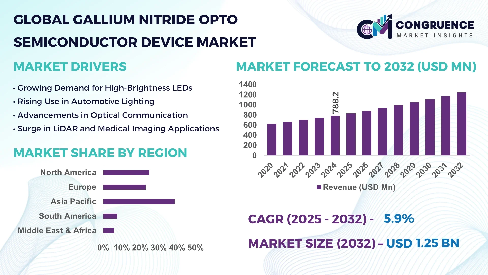
The Global Gallium Nitride Opto Semiconductor Device Market was valued at USD 788.2 Million in 2024 and is anticipated to reach a value of USD 1246.82 Million by 2032 expanding at a CAGR of 5.9% between 2025 and 2032.
To Learn More About This Report, Request A Free Sample Copy
China leads the global market with substantial production capacity, significant investment in advanced fabrication facilities, and a robust ecosystem supporting gallium nitride (GaN) technologies. The country’s manufacturing infrastructure is enhanced by state-of-the-art research centers focusing on optoelectronic innovations, enabling wide applications in telecommunications, automotive lighting, and power electronics. China's strategic advancements in GaN substrates and epitaxial growth processes further solidify its pivotal role in the Gallium Nitride Opto Semiconductor Device market.
The Gallium Nitride Opto Semiconductor Device market is strongly influenced by demand from sectors such as consumer electronics, aerospace, and industrial automation. High-performance GaN-based LEDs and laser diodes are driving efficiency improvements in optical communications and solid-state lighting. Regulatory frameworks emphasizing energy-efficient technologies and low environmental impact support the adoption of GaN devices. Technological breakthroughs, including enhanced thermal management and miniaturization of devices, are expanding market applications. Regional consumption varies, with Asia-Pacific showing accelerated growth due to rising industrial automation, while North America focuses on high-reliability aerospace uses. Emerging trends highlight integration of GaN devices in 5G networks and electric vehicles, forecasting robust development and diversification within the Gallium Nitride Opto Semiconductor Device market.
Artificial intelligence (AI) is increasingly shaping the Gallium Nitride Opto Semiconductor Device Market by revolutionizing manufacturing efficiency, quality control, and product design. AI-powered process automation and machine learning algorithms optimize epitaxial layer growth, reducing defect rates and enhancing yield consistency. Advanced AI-driven data analytics enable real-time monitoring and predictive maintenance of semiconductor fabrication equipment, minimizing downtime and improving operational performance. Within the Gallium Nitride Opto Semiconductor Device Market, AI-assisted simulation tools accelerate new device design cycles, allowing faster prototyping and deployment of innovative optoelectronic components.
Furthermore, AI integration enhances supply chain management by forecasting material demand, optimizing inventory, and streamlining logistics, thereby reducing costs and improving responsiveness to market fluctuations. The Gallium Nitride Opto Semiconductor Device Market benefits from AI applications in quality assurance where computer vision systems inspect wafers and devices for minute defects that human inspection might miss, ensuring higher product reliability and customer satisfaction. Across the market, AI fosters the development of smarter, more efficient GaN devices tailored to emerging industrial applications such as autonomous vehicles, smart lighting, and next-generation communication systems, solidifying its transformative impact on this rapidly evolving sector.
“In 2024, a leading semiconductor manufacturer implemented an AI-driven defect detection system in its GaN wafer fabrication process, resulting in a 30% reduction in production defects and a 15% increase in throughput efficiency, setting new industry standards for quality and operational excellence within the Gallium Nitride Opto Semiconductor Device Market.”
Rising global emphasis on sustainability and energy conservation is a crucial driver for the Gallium Nitride Opto Semiconductor Device market. GaN devices offer superior energy efficiency compared to traditional semiconductor technologies, enabling significant reductions in power consumption across lighting, automotive, and communication sectors. For example, GaN LEDs consume up to 50% less energy than conventional lighting systems, driving adoption in both commercial and residential applications. Additionally, the superior thermal conductivity and power handling of GaN components support their use in power electronics for electric vehicles and renewable energy systems. These factors collectively stimulate investments and product development, reinforcing GaN’s position as a preferred opto semiconductor material.
Despite the promising benefits, the Gallium Nitride Opto Semiconductor Device market faces challenges related to the high complexity of manufacturing GaN substrates and epitaxial layers. Producing defect-free GaN wafers requires sophisticated equipment and stringent quality controls, resulting in elevated production costs compared to silicon alternatives. This complexity can limit large-scale manufacturing capabilities and increase the final product price, creating entry barriers for new manufacturers and restraining widespread adoption. Furthermore, limited availability of high-quality bulk GaN substrates and supply chain constraints add to market pressures, slowing down production expansion and pricing competitiveness in cost-sensitive applications.
The rapid rollout of 5G networks and the future evolution toward 6G present significant growth opportunities for the Gallium Nitride Opto Semiconductor Device market. GaN devices are critical in enabling high-frequency, high-power performance necessary for advanced wireless communication systems. Their use in RF components, laser diodes, and photodetectors improves signal integrity and reduces energy losses in communication base stations and data centers. As telecommunications companies invest heavily in upgrading infrastructure to support higher data speeds and capacity, the demand for GaN-based optoelectronic devices is expected to grow substantially. This trend opens avenues for product innovation, market expansion, and strategic partnerships within the opto semiconductor ecosystem.
The Gallium Nitride Opto Semiconductor Device market encounters challenges related to evolving regulatory requirements and the lack of standardized manufacturing protocols. Diverse regulations across regions regarding materials handling, environmental compliance, and electronic device safety can complicate global market operations. Additionally, the absence of universal technical standards for GaN device fabrication and testing hampers interoperability and increases development costs. This fragmentation slows down industry-wide adoption and integration into complex systems. Companies must navigate complex certification processes and invest in R&D to meet stringent quality and safety norms, which can extend time-to-market and elevate operational expenditures.
• Expansion of High-Power GaN Laser Diodes: The Gallium Nitride Opto Semiconductor Device market is witnessing a surge in the deployment of high-power GaN laser diodes used in industrial manufacturing and medical imaging. Devices capable of emitting higher optical power with improved beam quality are meeting growing requirements in precision cutting and advanced diagnostic equipment. Production of GaN laser diodes with output powers exceeding 10 watts has increased by over 25% in the past year, highlighting advancements in device performance and manufacturing techniques.
• Integration of GaN Devices in Electric Vehicles: The automotive sector is increasingly integrating GaN-based optoelectronic components into electric vehicle systems, particularly for LiDAR sensors and adaptive lighting. This trend reflects a shift towards lighter, more energy-efficient components that enhance vehicle range and safety. Recent industry reports indicate that over 40% of new electric vehicle models launched in 2024 incorporate GaN-based optical modules, underscoring the material's critical role in automotive innovation.
• Growth of GaN-Based Optical Sensors for IoT Applications: GaN optoelectronic sensors are becoming essential for Internet of Things (IoT) devices requiring high sensitivity and low power consumption. These sensors enable precise environmental monitoring and smart infrastructure management. Market activity shows a 30% increase in shipments of GaN optical sensors used in smart city projects across Asia-Pacific and North America, reflecting expanding adoption in connected technologies.
• Advancements in Thermal Management Technologies: Enhanced thermal management solutions are being integrated with Gallium Nitride Opto Semiconductor Devices to address heat dissipation challenges inherent to high-power operation. Innovative cooling materials and micro-channel heat sinks have improved device reliability and longevity, with reported operating temperature reductions of up to 15%. These technological improvements are crucial for sustaining performance in demanding industrial and telecommunication environments.
The Gallium Nitride Opto Semiconductor Device market segmentation encompasses product types, applications, and end-user categories, each contributing uniquely to market development. Product types range from LEDs, laser diodes, photodetectors, to optical sensors, each serving distinct technical functions. Applications include telecommunications, automotive, consumer electronics, industrial automation, and healthcare, highlighting the versatility of GaN devices. End-users span sectors such as manufacturing, automotive OEMs, telecom infrastructure providers, and medical device companies. Understanding these segments allows decision-makers to tailor strategies aligned with specific market demands, technological advancements, and emerging industry trends influencing purchase behavior and investment focus within the Gallium Nitride Opto Semiconductor Device market.
The Gallium Nitride Opto Semiconductor Device market includes several primary product types: LEDs, laser diodes, photodetectors, and optical sensors. LEDs remain the leading type due to their extensive use in solid-state lighting, display technology, and communication devices. Their superior energy efficiency and long lifespan have solidified their widespread adoption in commercial and residential lighting. Laser diodes represent the fastest-growing type, driven by increasing demand in industrial manufacturing for precision cutting, medical diagnostics, and data communication. Recent enhancements in GaN laser diode power output and wavelength tuning capabilities accelerate this growth. Photodetectors, though niche, are critical for optical communication and sensing applications, while optical sensors are gaining traction in IoT and environmental monitoring systems, contributing steadily to market diversification.
Telecommunications stand as the leading application segment for Gallium Nitride Opto Semiconductor Devices, driven by the need for high-frequency and high-power components in 5G infrastructure and data centers. GaN devices enhance signal quality and energy efficiency in optical transceivers and base stations, making them indispensable. The fastest-growing application is automotive, where GaN-based optoelectronic devices support advanced driver-assistance systems (ADAS), LiDAR, and adaptive lighting technologies. The rise of electric vehicles and autonomous driving accelerates adoption in this sector. Other applications include consumer electronics, leveraging GaN LEDs for display backlighting and flash modules, industrial automation using GaN lasers for precision tasks, and healthcare, where GaN devices enable advanced imaging and diagnostic tools.
The manufacturing sector is the leading end-user of Gallium Nitride Opto Semiconductor Devices, utilizing them extensively in industrial automation, precision machining, and semiconductor fabrication tools. The robustness and energy efficiency of GaN devices meet the demanding operational requirements of this sector. The fastest-growing end-user segment is automotive original equipment manufacturers (OEMs), propelled by the electrification trend and increasing integration of GaN optoelectronic components in vehicle safety and sensing systems. Telecommunications infrastructure providers also constitute a significant end-user base, deploying GaN devices in network upgrades and expansions. Additionally, healthcare equipment manufacturers contribute notably by incorporating GaN-based lasers and sensors into diagnostic imaging and therapeutic devices, enhancing medical technology capabilities.
Asia-Pacific accounted for the largest market share at 38.7% in 2024 however, Asia-Pacific is expected to register the fastest growth, expanding at a CAGR of 7.1% between 2025 and 2032.
To Learn More About This Report, Request A Free Sample Copy
The Asia-Pacific region dominates the Gallium Nitride Opto Semiconductor Device market due to its expansive manufacturing infrastructure, high investment levels in semiconductor fabrication, and aggressive technology adoption in countries like China, Japan, and South Korea. Key industry sectors such as telecommunications, automotive, and consumer electronics significantly drive demand. The regional consumption pattern is strongly influenced by rapid urbanization, increasing demand for energy-efficient optoelectronic devices, and supportive government policies fostering innovation and production capacity expansion across the region.
Innovative Leadership in High-Performance Optoelectronics
North America holds approximately 27.3% of the Gallium Nitride Opto Semiconductor Device market volume, fueled by advanced industrial sectors including aerospace, defense, and healthcare. The region benefits from supportive government initiatives aimed at strengthening semiconductor supply chains and fostering research in next-generation GaN technologies. Regulatory frameworks focusing on energy efficiency and environmental sustainability are influencing market demand. Technological advancements such as integration of digital manufacturing and AI-driven process optimization are accelerating product innovation and operational efficiency. The widespread adoption of GaN-based components in 5G networks and autonomous vehicle technologies further propels regional market expansion.
Driving Sustainable and Smart Optoelectronics Innovation
Europe accounts for roughly 19.5% of the Gallium Nitride Opto Semiconductor Device market, with Germany, the UK, and France leading consumption. The region is marked by stringent regulatory standards from bodies promoting energy-saving and low-emission technologies, shaping the development and application of GaN devices. Sustainability initiatives have accelerated adoption of eco-friendly semiconductor manufacturing. Europe's advanced automotive and telecommunication sectors are key consumers of GaN optoelectronics. Moreover, the integration of emerging technologies such as Industry 4.0 and IoT within manufacturing hubs is reinforcing Europe’s position as a critical innovation center for GaN semiconductor devices.
Emerging Manufacturing Powerhouse and Innovation Hub
Asia-Pacific commands a market volume of approximately 39.1% in Gallium Nitride Opto Semiconductor Devices, with China, India, and Japan being the primary consumers. This region leads due to massive investments in semiconductor foundries, rapidly expanding electronics manufacturing clusters, and an increasing focus on developing smart cities and digital infrastructure. Manufacturing trends emphasize automation and precision fabrication to meet rising demand from consumer electronics, automotive, and telecommunication industries. Innovation hubs in the region are pioneering novel GaN applications, such as high-efficiency power amplifiers and UV optoelectronics, positioning Asia-Pacific as a pivotal growth arena.
Strategic Expansion Amidst Infrastructure Development
South America represents about 6.2% of the Gallium Nitride Opto Semiconductor Device market, with Brazil and Argentina as the key contributors. The regional market is influenced by growing infrastructure projects and increasing deployment of GaN-based lighting and sensing technologies in energy and construction sectors. Government incentives aimed at boosting local manufacturing and technology adoption are encouraging market growth. Trade policies favoring technological imports and partnerships are further supporting the integration of advanced GaN semiconductor solutions across diverse industrial applications, enhancing regional competitiveness.
Modernizing Optoelectronics for Energy and Construction Sectors
The Middle East & Africa market accounts for approximately 7.9% of Gallium Nitride Opto Semiconductor Devices consumption, with countries like the UAE and South Africa leading demand. The regional market growth is driven by extensive oil & gas infrastructure modernization and expanding construction activities requiring high-efficiency lighting and sensing solutions. Technological modernization initiatives are promoting the adoption of GaN optoelectronics in smart infrastructure projects. Local regulations emphasizing energy efficiency and new trade partnerships facilitating technology transfer support increasing penetration of GaN devices in critical sectors.
China: Holds 23.4% market share due to its massive semiconductor manufacturing capacity and strong domestic demand across telecommunications and consumer electronics industries.
United States: Captures 19.6% market share supported by advanced R&D ecosystems, strategic government programs, and high adoption rates in aerospace, defense, and automotive sectors.
The Gallium Nitride Opto Semiconductor Device market features a competitive landscape with over 30 active global players vying for leadership across various product segments and geographic regions. Market positioning is shaped by companies’ focus on technological innovation, strategic partnerships, and expanding manufacturing capabilities. Recent years have witnessed a surge in collaborative ventures between semiconductor manufacturers and technology firms aimed at accelerating the development of high-efficiency GaN devices for applications such as 5G infrastructure, automotive lighting, and power electronics. Product launches emphasize miniaturization, enhanced thermal management, and improved optical performance. Mergers and acquisitions continue to reshape the market, with several mid-sized firms consolidating to strengthen their R&D and production resources. Innovation trends such as integration of GaN devices with AI-driven process controls and new substrate materials are influencing competitive dynamics. Companies are also prioritizing sustainability initiatives in manufacturing to align with evolving regulatory requirements and customer expectations, further intensifying market competition.
Cree, Inc.
Infineon Technologies AG
OSRAM Opto Semiconductors GmbH
STMicroelectronics N.V.
NXP Semiconductors N.V.
Toshiba Corporation
Rohm Co., Ltd.
Epistar Corporation
II-VI Incorporated
Panasonic Corporation
The Gallium Nitride Opto Semiconductor Device market is being significantly influenced by advancements in epitaxial growth techniques, particularly Metal-Organic Chemical Vapor Deposition (MOCVD), which enable the production of high-quality GaN wafers with superior crystalline properties. These technological improvements contribute to enhanced efficiency and reliability in devices such as LEDs, laser diodes, and photodetectors. Additionally, innovations in substrate engineering—such as the use of silicon carbide (SiC) and bulk GaN substrates—are reducing defects and improving thermal management, crucial for high-power and high-frequency applications.
Emerging technologies also include the integration of GaN devices with photonic integrated circuits (PICs), which support miniaturization and improved signal processing in optical communication systems. Furthermore, advances in packaging technologies, like flip-chip bonding and wafer-level packaging, enhance device performance by reducing parasitic resistance and inductance. The development of flexible GaN optoelectronic components is opening new avenues in wearable and flexible electronics.
Automation and AI-driven process controls are being adopted in manufacturing to optimize yield and consistency. Finally, progress in ultraviolet (UV) GaN devices is expanding applications into water purification and sterilization, reflecting broader technological diversification that is shaping market dynamics for business leaders and industry professionals.
In March 2024, Cree announced the launch of its latest GaN-on-SiC high-electron-mobility transistor (HEMT) designed for enhanced power density and thermal performance in 5G base stations, enabling faster data transmission and lower energy consumption.
In September 2023, Infineon unveiled a new line of GaN-based power modules targeting automotive lighting and LiDAR applications, featuring improved durability and efficiency to meet stringent industry standards.
In November 2023, OSRAM introduced an advanced GaN UV LED platform aimed at expanding sterilization solutions in healthcare and water treatment sectors, offering higher output power with extended operational lifespan.
In May 2024, STMicroelectronics integrated AI-enabled quality inspection systems into its GaN wafer production line, reducing defect rates by 15% and enhancing overall device reliability for optoelectronic applications.
The Gallium Nitride Opto Semiconductor Device Market Report offers a comprehensive analysis of the market’s diverse segments, covering key product types such as LEDs, laser diodes, photodetectors, and ultraviolet devices. It explores applications across multiple industries, including telecommunications, automotive lighting, consumer electronics, healthcare, and industrial automation. The report provides detailed insights into end-user sectors, highlighting the adoption trends in manufacturing, energy, and environmental monitoring. Geographically, the report spans major regions including North America, Europe, Asia-Pacific, South America, and the Middle East & Africa, analyzing regional market shares, demand drivers, and infrastructure trends. It also addresses emerging markets within these regions, shedding light on growth prospects and innovation hubs.
From a technological perspective, the scope includes evaluation of epitaxial growth methods, substrate innovations, packaging advancements, and integration with photonic and electronic systems. The report further examines ongoing digital transformation efforts such as AI-driven manufacturing and quality control processes. Additionally, niche segments such as flexible GaN devices and ultraviolet sterilization technologies are covered, reflecting the market’s expanding application spectrum. This wide-ranging focus ensures the report provides decision-makers with strategic intelligence on market dynamics, competitive positioning, and future growth opportunities, enabling well-informed business planning and investment decisions.
| Report Attribute/Metric | Report Details |
|---|---|
|
Market Revenue in 2024 |
USD 788.2 Million |
|
Market Revenue in 2032 |
USD 1246.82 Million |
|
CAGR (2025 - 2032) |
5.9% |
|
Base Year |
2024 |
|
Forecast Period |
2025 - 2032 |
|
Historic Period |
2020 - 2024 |
|
Segments Covered |
By Types
By Application
By End-User
|
|
Key Report Deliverable |
Revenue Forecast, Growth Trends, Market Dynamics, Segmental Overview, Regional and Country-wise Analysis, Competition Landscape |
|
Region Covered |
North America, Europe, Asia-Pacific, South America, Middle East, Africa |
|
Key Players Analyzed |
Cree, Inc., Infineon Technologies AG, OSRAM Opto Semiconductors GmbH, STMicroelectronics N.V., NXP Semiconductors N.V., Toshiba Corporation, Rohm Co., Ltd., Epistar Corporation, II-VI Incorporated, Panasonic Corporation |
|
Customization & Pricing |
Available on Request (10% Customization is Free) |


