
Reports
The Global EUV Mask Inspection Market was valued at USD 1450 Million in 2025 and is anticipated to reach a value of USD 3293.71 Million by 2033 expanding at a CAGR of 10.8% between 2026 and 2033. Growth is being accelerated by increasing deployment of high-NA EUV lithography, stricter defect detection standards below 2 nm process nodes, and rising semiconductor fab investments supporting advanced mask quality control.
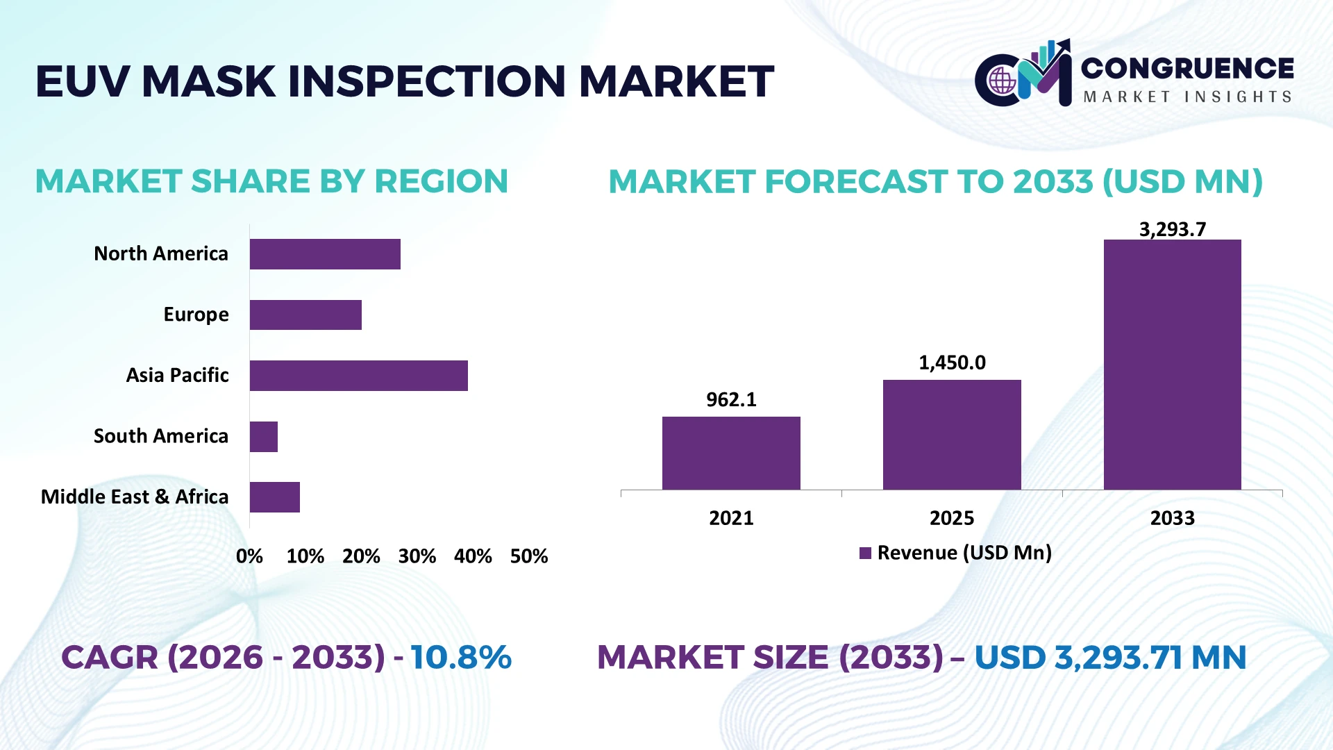
South Korea remains a dominant market, accounting for approximately 29% of advanced EUV mask inspection demand through strong memory and foundry manufacturing investments, while Japan contributes nearly 21% through precision optics, mask blank production, and inspection equipment capabilities. Ongoing semiconductor supply chain diversification following U.S.-Asia technology initiatives has accelerated capacity expansion, with automated inspection adoption exceeding 75% across leading advanced fabrication facilities, outpacing several European manufacturing hubs.
For technology suppliers and semiconductor manufacturers, expanding inspection accuracy, automation capabilities, and regional manufacturing partnerships remains a decisive competitive strategy.
Market Size & Growth: USD 1450 Million in 2025, projected to reach USD 3293.71 Million by 2033 at a CAGR of 10.8%, supported by high-NA EUV production and advanced semiconductor scaling.
Top Growth Drivers: Defect sensitivity improved by over 35%, AI-assisted inspection adoption exceeded 45%, and advanced wafer production capacity expanded by nearly 28%.
Short-Term Forecast: By 2028, automated inspection workflows reduce inspection cycle time by approximately 30% while improving defect detection efficiency by 22%.
Emerging Technologies: AI-based defect classification, multi-beam inspection platforms, and high-resolution optical systems improve inspection accuracy by more than 25% across advanced fabs.
Regional Leaders: Asia Pacific approaches USD 1850 Million with rapid fab expansion, North America exceeds USD 760 Million through domestic semiconductor investment, and Europe reaches nearly USD 480 Million driven by advanced equipment manufacturing.
Consumer/End-User Trends: More than 70% of leading semiconductor manufacturers prioritize automated EUV mask inspection for advanced logic and memory production.
Pilot/Case Example: During 2026, automated defect analytics reduced false defect identification by nearly 32% while improving inspection throughput by 24% in advanced manufacturing environments.
Competitive Landscape: KLA leads with an estimated 38% market share, alongside Lasertec, Applied Materials, ASML, and Hitachi High-Tech strengthening advanced inspection capabilities.
Regulatory & ESG Impact: Semiconductor localization policies increase regional equipment investment by over 20%, while optimized inspection processes reduce mask rework by approximately 18%.
Investment & Funding: More than USD 5 Billion supports semiconductor inspection ecosystems through strategic partnerships, fabrication expansion, and precision manufacturing initiatives amid global supply chain diversification.
Innovation & Future Outlook: Next-generation high-NA EUV inspection, AI-driven analytics, and digital manufacturing platforms improve operational precision by over 30%, reinforcing long-term competitive positioning.
The EUV Mask Inspection Market is advancing through demand from advanced logic, memory, and semiconductor foundry production, where defect-free mask verification has become a manufacturing priority. AI-enabled defect analytics and high-NA compatible inspection platforms have improved inspection productivity by approximately 25%, while semiconductor localization programs and resilient supply-chain strategies continue accelerating equipment deployment. These technology and investment trends establish the foundation for the following strategic market discussion.
The EUV Mask Inspection Market has become strategically important as semiconductor manufacturers compete to achieve reliable sub-2 nm production while reducing defect-related yield losses. Supply-chain restructuring and semiconductor localization initiatives across the United States, Japan, and South Korea are accelerating investment in advanced inspection ecosystems to secure manufacturing resilience. Digital inspection platforms integrated with AI analytics are becoming a competitive differentiator, enabling faster process qualification and reducing production interruptions across high-volume fabrication facilities.
Modern AI-assisted multi-beam inspection systems improve defect classification accuracy by approximately 30% while reducing inspection cycle times by nearly 25% compared with conventional optical inspection workflows. Japan maintains leadership in precision mask manufacturing and inspection technologies, whereas South Korea focuses on rapid deployment within high-volume memory fabrication. Over the next two to three years, automated inspection penetration is expected to exceed 80% among leading advanced semiconductor fabs as high-NA EUV production expands and data-driven quality management becomes standard practice.
A practical example is the integration of automated defect review with manufacturing execution systems, allowing engineers to shorten mask qualification cycles and improve production consistency. Equipment suppliers are expanding technology partnerships, localized service capabilities, and joint development programs with semiconductor manufacturers to strengthen long-term competitiveness. Companies that combine advanced inspection accuracy with scalable automation and regional collaboration will secure stronger operational resilience and strategic market positioning.
Transition toward high-NA EUV lithography is reshaping inspection requirements as manufacturers target smaller process nodes with tighter defect tolerances. AI-assisted inspection platforms improve defect identification by approximately 32%, while automated review reduces manual analysis time by nearly 28%. More than 70% of advanced semiconductor projects now incorporate automated inspection planning during process qualification. Japan continues strengthening domestic mask manufacturing capabilities through precision engineering investments, while U.S. semiconductor expansion policies support localized equipment ecosystems. This combination of technology advancement and supply-chain resilience is encouraging equipment vendors to increase R&D spending, establish collaborative development programs, and expand local service networks. Companies that integrate AI-enabled analytics with high-resolution inspection platforms gain measurable improvements in production yield, customer qualification speed, and long-term manufacturing reliability.
The market faces structural limitations from concentrated component sourcing, demanding qualification requirements, and limited supplier availability for high-precision optical systems. Specialized subsystem procurement accounts for nearly 45% of equipment lead-time variation, while precision component costs fluctuate by approximately 18% due to constrained manufacturing capacity. Export control measures affecting advanced semiconductor technologies continue influencing procurement strategies and cross-border equipment deployment. These conditions increase operational planning complexity, extend installation schedules, and delay production readiness for new fabrication facilities. Companies are mitigating these pressures through localized supplier partnerships, multi-source procurement strategies, and longer-term component agreements. Organizations capable of reducing dependency on single-source precision components improve deployment predictability and strengthen operational continuity during supply-chain disruptions.
AI-driven predictive inspection, digital twin integration, and cloud-enabled manufacturing analytics are opening new opportunities beyond traditional defect detection. Automated workflow optimization improves equipment utilization by approximately 22%, while predictive maintenance reduces unplanned downtime by nearly 20%. India and Singapore are strengthening semiconductor ecosystem initiatives that encourage technology collaboration, engineering capability development, and localized manufacturing support. Equipment manufacturers are responding by expanding software-based inspection solutions, establishing joint innovation centers, and developing interoperable analytics platforms compatible with next-generation fabrication environments. A notable strategic opportunity lies in combining inspection intelligence with factory-wide production analytics, enabling continuous process optimization instead of isolated quality control. This integrated approach strengthens customer retention while creating higher-value service and software revenue streams.
Executing advanced inspection at future technology nodes requires significantly higher computational capability, skilled engineering resources, and seamless integration with increasingly automated fabrication environments. Data volumes generated during inspection increase by nearly 40% with advanced mask designs, while engineering talent shortages affect approximately 25% of specialized semiconductor manufacturing roles in several technology-intensive economies. Maintaining consistent inspection performance across geographically distributed fabrication sites also increases operational complexity. Companies are addressing these challenges through AI-assisted decision support, workforce development programs, standardized software architectures, and strategic partnerships with research institutions. Organizations that successfully combine scalable digital infrastructure with specialized engineering expertise will achieve more consistent deployment, stronger manufacturing resilience, and sustainable competitive differentiation in advanced semiconductor production.
AI-Driven Defect Intelligence Advanced AI-enabled defect classification is becoming standard across leading semiconductor fabs, improving detection accuracy by approximately 30% while reducing manual review effort by nearly 35%. The transition toward high-NA EUV production is increasing data complexity, prompting manufacturers in Japan and South Korea to integrate machine learning directly into inspection workflows. Equipment vendors are expanding AI software partnerships and cloud-enabled analytics to shorten engineering response times, improve process consistency, and accelerate mask release without increasing inspection labor.
High-NA Inspection Readiness Migration toward next-generation EUV lithography is driving inspection platform upgrades capable of handling smaller feature geometries. More than 65% of newly planned advanced inspection installations are designed with high-NA compatibility, while automated calibration improves measurement repeatability by nearly 20%. Semiconductor localization policies in the United States are accelerating equipment modernization, encouraging suppliers to redesign optical architectures and strengthen long-term service capabilities for advanced manufacturing environments.
Localized Service Network Expansion Supply-chain resilience has shifted attention beyond equipment manufacturing toward regional engineering support and lifecycle services. Local technical support centers reduce equipment downtime by approximately 18%, while predictive maintenance improves utilization rates by nearly 22%. Global inspection vendors are expanding partnerships with domestic semiconductor manufacturers and component suppliers, enabling faster deployment, improved spare-parts availability, and stronger operational continuity despite ongoing geopolitical technology restrictions.
Integrated Smart Factory Inspection Inspection platforms are increasingly connected with manufacturing execution systems and factory-wide analytics, allowing automated feedback across production lines. Digital workflow integration reduces process verification time by approximately 25% and improves overall production efficiency by nearly 19%. Manufacturers are standardizing interoperable software architectures and collaborative automation strategies, creating a less visible but significant competitive advantage through synchronized quality control rather than standalone inspection performance.
Multi-Beam Inspection holds the leading position with an estimated 37% market share because it delivers superior throughput, higher defect sensitivity, and scalable inspection performance for advanced semiconductor nodes. Its ability to inspect complex EUV masks with greater productivity makes it the preferred solution for high-volume manufacturing. Optical Inspection remains widely deployed for routine production monitoring because of its lower operational complexity and established integration across mature fabrication facilities. Companies continue improving both technologies through AI-assisted image processing and higher-resolution optical architectures to extend inspection capability without disrupting existing production infrastructure.
Actinic Inspection is the fastest-growing segment as semiconductor manufacturers require inspection under EUV wavelengths to identify buried defects that conventional systems cannot detect. Adoption has increased by approximately 24% across advanced research and pilot production environments, while Multi-Beam productivity improvements exceed 28% through parallel processing architectures. E-Beam Inspection continues serving high-precision defect analysis where ultimate sensitivity outweighs inspection speed. Equipment suppliers are prioritizing product innovation, joint technology programs, and specialized platform development to strengthen competitive differentiation as investment shifts toward next-generation inspection ecosystems.
Defect Inspection accounts for approximately 42% of market demand as semiconductor manufacturers prioritize early identification of printable defects that directly affect wafer yield and production stability. Automated inspection platforms reduce false defect identification by nearly 30%, improving engineering productivity and shortening production qualification cycles. Process Control continues serving mature manufacturing operations by maintaining inspection consistency across production lots, while Mask Qualification remains essential before high-value masks enter volume manufacturing. Companies are integrating AI-assisted analytics with factory automation to accelerate decision-making and improve manufacturing reliability.
Yield Improvement is the fastest-growing application as advanced semiconductor facilities increasingly connect inspection results with process optimization platforms. Automated yield analytics improve production consistency by approximately 22%, while integrated process feedback reduces corrective engineering cycles by nearly 18%. Manufacturers are expanding deployment of closed-loop inspection architectures that connect defect analysis directly with lithography and manufacturing execution systems. This operational integration strengthens productivity, reduces waste, and supports continuous quality optimization across increasingly complex semiconductor manufacturing environments.
Semiconductor Foundries represent the largest end-user segment with an estimated 46% market share due to continuous investment in leading-edge logic production and advanced EUV lithography infrastructure. High-volume manufacturing requires continuous mask inspection to maintain production consistency and minimize yield loss. Integrated Device Manufacturers remain significant buyers as they strengthen internal semiconductor production capabilities and modernize fabrication facilities. Equipment suppliers increasingly customize software, automation features, and long-term service agreements to meet the operational requirements of large manufacturing organizations.
Photomask Manufacturers represent the fastest-growing end-user segment as tighter design tolerances and high-NA EUV adoption increase demand for advanced mask verification. Automated inspection deployment has expanded by approximately 27%, while digital workflow integration improves qualification efficiency by nearly 21%. Research Institutes continue supporting early-stage technology validation and next-generation inspection innovation through collaborative development initiatives. Companies are strengthening ecosystem partnerships, localized engineering support, and application-specific platform customization to capture demand across both commercial production and advanced research environments.
Asia-Pacific accounted for the largest market share at 48% in 2025 however, North America is expected to register the fastest growth, expanding at a 12.1% between 2026 and 2033.

Advanced Fab Expansion Drives Inspection Modernization
North America represents approximately 24% of global EUV mask inspection deployment, supported by expanding advanced semiconductor manufacturing capacity and sustained investment in domestic fabrication infrastructure. The United States continues accelerating inspection system deployment through new wafer fabrication projects and advanced packaging facilities requiring higher mask quality standards. More than 68% of newly commissioned leading-edge fabs in the region are integrating AI-enabled inspection platforms into production qualification workflows. Equipment suppliers are strengthening regional engineering centers, localized technical support, and strategic partnerships with semiconductor manufacturers to reduce deployment timelines and improve operational continuity. Increasing collaboration between equipment developers and foundries is also shortening technology validation cycles while supporting faster adoption of high-NA EUV manufacturing capabilities.
United States Market Outlook: The United States remains the regional technology leader through extensive semiconductor manufacturing expansion, advanced equipment development, and national supply-chain resilience initiatives. More than 70% of North America's leading-edge semiconductor investment is concentrated in the country, encouraging deployment of next-generation inspection platforms and localized engineering support. Equipment vendors continue expanding collaborative R&D programs with foundries and research organizations, strengthening long-term manufacturing competitiveness while improving technology commercialization.
Precision Engineering Strengthens Technology Leadership
Europe accounts for nearly 21% of global market activity, supported by advanced lithography expertise, precision optics manufacturing, and semiconductor equipment innovation. Regional demand is driven by continuous modernization of semiconductor production capabilities and stronger collaboration between equipment suppliers and research institutions. Automated inspection integration has increased by approximately 26% across advanced manufacturing programs, improving qualification efficiency and production consistency. Companies are investing in precision metrology, digital inspection software, and collaborative engineering programs to support future high-NA EUV deployment while maintaining high manufacturing standards. Sustainability initiatives are also encouraging energy-efficient inspection platforms with optimized equipment utilization across semiconductor production facilities.
Netherlands Market Outlook: The Netherlands maintains strategic importance through world-leading lithography technology, advanced optics expertise, and semiconductor equipment innovation. More than 60% of Europe's advanced EUV equipment ecosystem is linked to Dutch technology development and supplier networks. Continued investment in collaborative engineering, precision manufacturing, and ecosystem partnerships strengthens the country's role as a critical innovation hub for next-generation mask inspection solutions.
Manufacturing Scale Accelerates Technology Deployment
Asia-Pacific contributes approximately 48% of global market demand due to its concentration of semiconductor foundries, memory manufacturers, and photomask production facilities. South Korea, Taiwan, Japan, and China continue expanding advanced semiconductor manufacturing infrastructure, increasing demand for highly automated inspection systems. More than 75% of advanced EUV manufacturing lines in the region operate with automated inspection workflows, improving production consistency and reducing qualification delays. Equipment suppliers are expanding manufacturing partnerships, regional service capabilities, and application engineering centers to support rapidly increasing deployment volumes. Strong export-oriented semiconductor production and continuous investment in advanced process technologies reinforce the region's leadership across the global inspection ecosystem.
South Korea Market Outlook: South Korea remains the most strategically significant country due to its leadership in memory semiconductor production and advanced fabrication deployment. Automated inspection adoption exceeds 80% across leading high-volume manufacturing facilities, supported by continuous investment in process optimization and AI-enabled quality control. Equipment vendors continue expanding local engineering teams and collaborative development initiatives to improve production yield and strengthen next-generation manufacturing competitiveness.
Emerging Semiconductor Infrastructure Creates Demand
South America represents a developing market where semiconductor research, electronics manufacturing, and industrial modernization are gradually increasing demand for advanced inspection technologies. Brazil accounts for the largest regional deployment activity through government-supported electronics manufacturing initiatives and technology partnerships. Approximately 58% of regional semiconductor-related investment is concentrated in industrial clusters supporting design, testing, and component manufacturing. Infrastructure limitations and dependence on imported advanced equipment continue influencing deployment speed, prompting companies to prioritize technical partnerships, localized support services, and phased technology implementation. Regional enterprises increasingly focus on strengthening engineering capability before expanding advanced semiconductor manufacturing capacity.
Brazil Market Outlook: Brazil leads the regional market through its established electronics manufacturing ecosystem and growing semiconductor policy initiatives. Industrial modernization programs continue encouraging technology collaboration with international equipment suppliers, while investment in engineering capability and advanced manufacturing infrastructure supports future inspection deployment. Local enterprises are expanding technical partnerships to improve production quality and prepare for higher-value semiconductor manufacturing activities.
Strategic Technology Investment Builds Capability
The Middle East & Africa remains an emerging market where semiconductor ecosystem development is supported by national technology diversification strategies and research infrastructure expansion. Regional deployment is concentrated in innovation programs, technology parks, and advanced manufacturing initiatives rather than large-scale semiconductor production. Approximately 40% of recent semiconductor-related investment targets research infrastructure, digital manufacturing capability, and engineering development. International technology partnerships are strengthening access to advanced inspection expertise while supporting knowledge transfer and workforce development. Companies are prioritizing long-term collaboration over immediate production expansion, positioning the region for gradual participation in advanced semiconductor value chains.
Saudi Arabia Market Outlook: Saudi Arabia is strengthening its position through industrial diversification programs, advanced technology investments, and semiconductor ecosystem development. National innovation initiatives continue supporting research centers, engineering capability, and strategic technology partnerships. Investment in digital manufacturing infrastructure and collaborative industrial projects is creating a stronger foundation for future adoption of advanced semiconductor inspection technologies while expanding regional technical expertise.
The competitive landscape is led by KLA, Lasertec, Applied Materials, Hitachi High-Tech, and ASML, while specialized metrology developers compete through niche inspection capabilities and engineering customization. The top five players collectively control approximately 82% of the market, reflecting strong technology concentration and high entry barriers. Global leaders compete through inspection resolution, AI-enabled analytics, and integrated software platforms, whereas emerging technology providers differentiate with application-specific innovation and faster engineering support. Equipment performance improvements exceeding 25% and automated defect classification gains above 30% have shifted competition from hardware alone toward intelligent inspection ecosystems. Companies are expanding through strategic partnerships with semiconductor foundries, localized engineering centers, joint technology development, and tighter integration with manufacturing execution systems. Vertical integration across optics, software, and service capabilities is strengthening customer retention while reducing deployment complexity. Winning in this market requires superior inspection precision, scalable automation, resilient supply chains, and deep collaboration with advanced semiconductor manufacturers.
KLA Corporation
Lasertec Corporation
ASML Holding N.V.
Applied Materials, Inc.
Hitachi High-Tech Corporation
JEOL Ltd.
Nikon Corporation
Carl Zeiss AG
Onto Innovation Inc.
Advantest Corporation
Hamamatsu Photonics K.K.
SCREEN Holdings Co., Ltd.
Toray Engineering Co., Ltd.
Hermes Microvision (HMI)
Current EUV mask inspection platforms combine high-resolution optics, AI-enabled defect classification, and automated metrology to support advanced semiconductor manufacturing below the 2 nm node. AI-assisted inspection improves defect detection accuracy by approximately 30% while reducing manual review time by nearly 35%. More than 70% of leading-edge semiconductor fabs are integrating automated inspection into production qualification workflows. Compared with conventional optical inspection, modern multi-beam architectures deliver nearly 28% higher throughput while maintaining tighter defect sensitivity, giving manufacturers measurable yield and cycle-time advantages.
Emerging technologies between 2026 and 2028 include high-NA compatible actinic inspection, digital twin-enabled process monitoring, and cloud-connected inspection analytics. High-NA inspection systems improve printable defect identification by approximately 22%, while predictive analytics reduce unplanned inspection downtime by nearly 18%. Adoption of integrated manufacturing execution system connectivity has surpassed 60% among advanced fabrication facilities, enabling real-time quality feedback. Equipment suppliers are expanding software-defined inspection platforms that combine image analytics, process intelligence, and automated defect classification into unified operational environments.
Disruptive innovation is shifting competition toward intelligent inspection ecosystems rather than standalone hardware performance. Companies investing in AI algorithms, high-speed multi-beam architectures, and interoperable factory software gain faster qualification cycles, lower engineering workloads, and stronger customer retention. Technology leaders capable of integrating inspection, analytics, and production automation will establish sustainable competitive advantages as high-NA EUV manufacturing scales globally through 2028.
December 2025 Lasertec Corporation introduced the MAGICS M9750 and M9751 mask blank inspection systems featuring new inspection optics and high-speed circuitry for higher sensitivity and throughput, strengthening next-generation EUV mask qualification capabilities. Source: Lasertec
October 2025 Lasertec Corporation launched the ACTIS A200HiT actinic EUV patterned mask inspection platform delivering 3× inspection speed versus the previous ACTIS A150, enabling faster wafer-fab quality assurance and lower inspection costs.
December 2024 Lasertec Corporation released the ABICS Series E320 EUV mask blank inspection and review system with 1,500× high-magnification review capability, improving phase-defect detection accuracy for high-NA EUV mask manufacturing.
December 2024 Lasertec Corporation introduced the PELMIS Series EUV pellicle inspection system with automatic front/back particle classification, enabling full-mask inspection workflows and improving productivity for advanced semiconductor manufacturing operations. Source: Lasertec
The report provides comprehensive coverage of the global EUV Mask Inspection Market across Actinic Inspection, Optical Inspection, E-Beam Inspection, and Multi-Beam Inspection technologies. It evaluates operational trends across Defect Inspection, Mask Qualification, Process Control, and Yield Improvement while assessing demand from Semiconductor Foundries, Integrated Device Manufacturers, Photomask Manufacturers, and Research Institutes. The study examines competitive technology adoption, with automated inspection deployment exceeding 70% across advanced semiconductor manufacturing and increasing integration of AI-enabled analytics into production workflows.
The analysis covers North America, Europe, Asia-Pacific, South America, and the Middle East & Africa, highlighting manufacturing concentration, technology deployment, supply-chain positioning, and emerging investment opportunities. It profiles leading equipment developers, evaluates innovation strategies, partnership activity, and inspection platform evolution, and delivers actionable insights for expansion planning, competitive benchmarking, technology selection, operational optimization, and long-term strategic positioning across advanced semiconductor manufacturing between 2026 and 2033.
| Report Attribute/Metric | Report Details |
|---|---|
Market Revenue in 2025 | USD 1450 Million |
Market Revenue in 2033 | USD 3293.71 Million |
CAGR (2026 - 2033) | 10.8% |
Base Year | 2025 |
Forecast Period | 2026 - 2033 |
Historic Period | 2021 - 2025 |
Segments Covered | By Type
By Application
By End-User
|
Key Report Deliverable | Revenue Forecast, Growth Trends, Market Dynamics, Segmental Overview, Regional and Country-wise Analysis, Competition Landscape |
Region Covered | North America, Europe, Asia-Pacific, South America, Middle East, Africa |
Key Players Analyzed | KLA Corporation, Lasertec Corporation, ASML Holding N.V., Applied Materials, Inc., Hitachi High-Tech Corporation, JEOL Ltd., Nikon Corporation, Carl Zeiss AG, Onto Innovation Inc., Advantest Corporation, Hamamatsu Photonics K.K., SCREEN Holdings Co., Ltd., Toray Engineering Co., Ltd., Hermes Microvision (HMI) |
Customization & Pricing | Available on Request (10% Customization is Free) |