
Reports
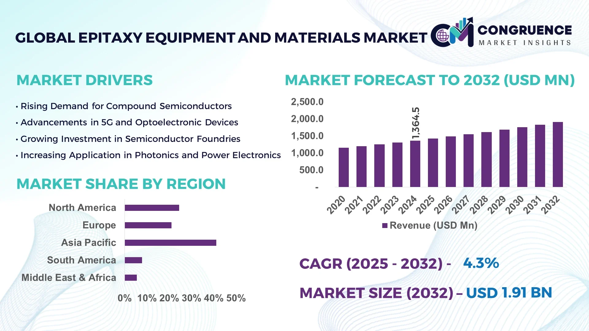
The Global Epitaxy Equipment and Materials Market was valued at USD 1364.45 Million in 2024 and is anticipated to reach a value of USD 1910.87 Million by 2032 expanding at a CAGR of 4.3% between 2025 and 2032.
In Japan, a global leader in semiconductor manufacturing equipment, major investments in silicon wafer epitaxy technology are enabling higher production throughput and integration with advanced photonics. The country’s manufacturing clusters have established world-class cleanroom infrastructure and robust R&D capabilities supporting next-generation epitaxial deposition processes.
The Epitaxy Equipment and Materials Market plays a pivotal role in driving innovation across high-growth sectors such as power electronics, optoelectronics, and RF device manufacturing. With increasing demand for gallium nitride (GaN) and silicon carbide (SiC)-based devices, manufacturers are investing in advanced epitaxial reactors that deliver superior crystal quality and wafer uniformity. Recent innovations in metal-organic chemical vapor deposition (MOCVD) and molecular beam epitaxy (MBE) are enhancing precision in layer growth for high-frequency and high-power applications. Moreover, regulatory support for renewable energy and electric mobility is accelerating the demand for epitaxial materials in solar and EV-related semiconductor components. Asia-Pacific leads in regional consumption, driven by aggressive infrastructure development and smart device proliferation, while Europe is witnessing a surge in R&D funding for compound semiconductor applications. Emerging trends include epitaxy-on-substrate (EOS) solutions and hybrid epitaxy techniques, signaling a transformative shift in the materials ecosystem and production standards.
Artificial intelligence is reshaping the Epitaxy Equipment and Materials Market by enabling smarter, faster, and more precise manufacturing processes. Through intelligent data analysis and predictive modeling, AI is enhancing epitaxial growth outcomes by optimizing process variables such as temperature, pressure, gas flow, and deposition rates. These AI-powered control systems are reducing material waste, minimizing defects, and improving uniformity in crystal layer formation, especially in the fabrication of advanced SiC and GaN wafers for power electronics and LED devices.
Real-time analytics powered by machine learning algorithms allow for dynamic process adjustments in epitaxial deposition equipment, leading to improved wafer yield and equipment uptime. This has proven especially beneficial for manufacturers seeking to meet tight tolerance requirements for high-frequency semiconductor devices. In addition, AI is streamlining maintenance operations by enabling predictive diagnostics, reducing unplanned downtimes, and extending equipment lifespan. Integration of AI into epitaxy reactors is also aiding in digital twin simulations that accelerate R&D timelines and support prototype scaling without interrupting production cycles.
As the Epitaxy Equipment and Materials Market evolves, AI is proving essential in driving competitive advantages through cost optimization, operational efficiency, and product quality. The convergence of AI and epitaxial process technology is fostering a new era of semiconductor fabrication that aligns with the high-precision demands of emerging applications such as quantum computing, 6G networks, and autonomous systems.
“In March 2024, a leading Japanese semiconductor equipment firm introduced an AI-driven epitaxy system featuring adaptive control algorithms that reduced defect density in GaN-on-Si wafers by 28%, significantly enhancing production yield for power device manufacturers.”
The growing demand for high-efficiency power devices in electric vehicles, renewable energy systems, and industrial automation is significantly boosting the adoption of silicon carbide (SiC) and gallium nitride (GaN) semiconductors. These materials require specialized epitaxy processes to produce high-quality crystal layers that meet performance standards for high-voltage and high-temperature operations. For instance, SiC-based MOSFETs and Schottky diodes offer superior switching speeds and thermal conductivity, necessitating advanced epitaxial equipment capable of managing tight growth parameters. As manufacturers strive to achieve compact designs with lower energy losses, the Epitaxy Equipment and Materials Market is witnessing an increased focus on horizontal and vertical epitaxy tools specifically configured for compound semiconductors. Furthermore, automakers and renewable energy solution providers are entering long-term contracts with wafer producers, accelerating capacity expansion and innovation in epitaxial process technologies.
One of the primary restraints affecting the Epitaxy Equipment and Materials Market is the substantial capital investment required for procuring and maintaining advanced epitaxy systems. High-precision reactors, especially those tailored for compound semiconductor applications, involve complex engineering and demand cleanroom environments, resulting in increased setup costs. Additionally, regular calibration, specialized components, and the need for skilled personnel further raise operational expenses. Small and mid-sized wafer fabrication units often face barriers to entry due to these cost constraints, slowing market adoption. Moreover, any technical faults or deviations during epitaxial growth can result in wafer defects, causing significant material loss and downtime. This risk adds to the total cost of ownership and discourages new market entrants. Manufacturers must therefore navigate high investment thresholds and manage operational efficiency without compromising yield or quality.
The Epitaxy Equipment and Materials Market stands to benefit from the strategic expansion of semiconductor manufacturing hubs in emerging economies like India, Vietnam, and Malaysia. These countries are increasingly offering policy incentives, tax benefits, and infrastructural support to attract global semiconductor companies. India, for instance, has launched national semiconductor missions, aiming to establish world-class fabs and epitaxy units to support local demand for electronics and defense technologies. The cost advantage in terms of labor and facility development, combined with rising domestic consumption of smartphones, EVs, and industrial automation systems, is prompting equipment manufacturers to localize production and service operations. Furthermore, public-private partnerships are facilitating technology transfer and joint ventures in these regions, opening avenues for scalable growth in epitaxial material production and equipment deployment. These factors create fertile ground for market penetration and capacity building.
Maintaining consistent epitaxial layer quality across large wafer diameters presents a major technical challenge in the Epitaxy Equipment and Materials Market. Uniformity in crystal growth is critical to device performance, and any deviation during deposition can lead to yield losses and increased testing requirements. As wafers scale up to 200mm and 300mm for power and RF applications, ensuring precision in temperature gradients, gas flow distribution, and pressure control becomes more complex. Additionally, each material system—whether GaN-on-Si, SiC, or InP—requires specific process recipes and environmental controls, increasing system customization needs. Scaling production without compromising layer integrity or throughput places considerable pressure on R&D and process engineering teams. The challenge is further amplified in pilot-scale operations transitioning to high-volume manufacturing, where maintaining reproducibility and defect reduction becomes mission-critical.
• Increased Demand for Compound Semiconductor Substrates: With the transition toward electric vehicles, 5G infrastructure, and high-efficiency power systems, there is a sharp uptick in demand for epitaxial layers on wide bandgap materials like gallium nitride (GaN) and silicon carbide (SiC). SiC substrates, in particular, are being used to produce MOSFETs and power modules capable of handling higher voltages with reduced thermal losses. In 2024 alone, SiC wafer production capacity expanded by over 30% in Asia-Pacific fabrication hubs, prompting parallel investments in advanced epitaxy reactors tailored for compound materials.
• Automation and Inline Metrology Integration in Epitaxy Tools: Manufacturers are increasingly adopting epitaxy equipment embedded with real-time metrology systems to monitor layer thickness, crystal quality, and uniformity. These integrated tools are streamlining quality assurance while reducing inspection times by up to 40%. Automated process calibration using AI-enhanced feedback loops has also become standard, enabling consistent performance even with wafer size scaling. This trend is especially prevalent in fabs producing 200mm and 300mm wafers for automotive and high-speed logic applications.
• Shift Toward Green Manufacturing Techniques: Environmental regulations are pushing epitaxy equipment manufacturers to develop reactors with lower gas consumption and minimal toxic byproduct generation. Low-pressure chemical vapor deposition (LPCVD) systems are increasingly being selected over legacy equipment due to their reduced environmental footprint. Adoption of hydrogen recovery systems and exhaust treatment modules has increased, especially among European fabs aiming to align with green technology standards.
• Expansion of Turnkey Epitaxy Production Lines: To meet the growing complexity of multilayer device structures, many semiconductor foundries are investing in full-stack epitaxy solutions that offer pre-configured, turnkey production lines. These integrated setups include wafer handling, cleaning, deposition, and annealing systems under a single workflow, improving throughput by up to 25%. This approach is gaining traction among mid-size fabs in Southeast Asia and Eastern Europe, aiming to enhance manufacturing flexibility and lower operational downtime.
The Epitaxy Equipment and Materials Market is segmented based on product type, application, and end-user industries. In terms of type, the market includes MOCVD systems, MBE systems, HVPE systems, and epitaxial wafers tailored for specific semiconductor needs. Applications span across LED manufacturing, power electronics, MEMS, RF devices, and laser diodes. Among end-users, the key participants include integrated device manufacturers (IDMs), foundries, and R&D institutions. The demand for high-quality epitaxial layers is being driven by advancements in electric mobility, renewable energy, and wireless communication systems. Equipment and material suppliers are tailoring solutions to meet the technical demands of SiC, GaN, and InP-based devices. Each segment reflects evolving technological priorities, with growing customization, substrate compatibility, and process integration driving differentiation and competitive positioning across the market landscape.
MOCVD (Metal-Organic Chemical Vapor Deposition) systems represent the leading product type in the Epitaxy Equipment and Materials Market due to their extensive application in the production of LEDs and GaN-based power devices. Their versatility and high throughput make them a standard choice for commercial-scale manufacturing. Molecular Beam Epitaxy (MBE), although more niche, is gaining traction for advanced research and precision-layer applications, particularly in quantum electronics and photonics. The fastest-growing type is the epitaxial wafers category, driven by surging demand for SiC and GaN substrates in EV inverters and 5G telecom components. HVPE (Hydride Vapor Phase Epitaxy) systems, while less common, are being adopted for thick GaN layers in laser diodes and optoelectronics. Innovations in multi-wafer batch reactors and hybrid epitaxy systems are also contributing to segment expansion by offering process flexibility and enhanced wafer yield.
Power electronics currently lead the application segment, propelled by the rapid adoption of SiC- and GaN-based components in electric vehicles, renewable energy converters, and industrial automation systems. These devices require high-quality epitaxial layers for performance stability under high-voltage conditions. The fastest-growing application is RF and microwave devices, which are seeing increased demand due to 5G infrastructure expansion and satellite communication development. LED manufacturing continues to hold a strong position, especially in Asia-Pacific, due to sustained demand for energy-efficient lighting and display technologies. Additionally, applications such as laser diodes and MEMS are gaining niche importance for specialized sectors like healthcare imaging and optical communication. The broadening scope of applications is fueling a need for customizable epitaxy systems that support various deposition techniques and materials.
Foundries dominate the end-user segment of the Epitaxy Equipment and Materials Market, primarily due to their large-scale production capabilities and active investment in compound semiconductor fabrication. These facilities prioritize high-throughput, scalable epitaxy systems that ensure consistency across multi-wafer batches. Integrated Device Manufacturers (IDMs) follow closely, benefiting from in-house process control and customized layer development aligned with proprietary chip architectures. The fastest-growing end-user category is research and development institutions, which are increasingly collaborating with commercial fabs and government programs to accelerate innovations in epitaxial materials. Their focus on prototyping and novel device structures contributes significantly to equipment refinement and material innovation. Emerging fabless startups and design firms are also influencing demand through outsourcing strategies, driving utilization of modular epitaxy services across the value chain.
Asia-Pacific accounted for the largest market share at 41.2% in 2024, however, North America is expected to register the fastest growth, expanding at a CAGR of 5.1% between 2025 and 2032.
The strong performance in Asia-Pacific is supported by high-volume wafer production, rising demand for GaN and SiC substrates, and government-backed semiconductor infrastructure in countries like China, Japan, and South Korea. Meanwhile, North America’s surge is fueled by rapid adoption of advanced epitaxy technologies across power electronics and defense applications. This regional divergence reflects differing economic priorities, policy environments, and levels of technological investment.
Advanced Manufacturing Initiatives Boosting Equipment Demand
In 2024, this region held approximately 24.7% of the global Epitaxy Equipment and Materials Market, largely driven by its established semiconductor ecosystem and heavy government investment in reshoring chip production. Key industries such as automotive electronics, aerospace, and industrial automation continue to stimulate demand for high-performance epitaxial materials. The CHIPS Act and other semiconductor incentive programs are providing tax benefits and funding to enhance domestic capacity. Advanced digital transformation in fab processes—including AI-driven metrology and defect analysis—has also accelerated adoption of next-gen epitaxy tools across several foundries and IDMs. These factors are combining to build a robust, innovation-led growth environment.
Green Tech Priorities Accelerate Compound Semiconductor Adoption
Europe contributed around 18.3% to the global Epitaxy Equipment and Materials Market in 2024, supported by national strategies aimed at reducing dependence on non-European chip suppliers. Germany, France, and the Netherlands are at the forefront, investing in fabs producing power devices and photonics components. Regulatory bodies such as the European Chips Act authority are encouraging sustainable manufacturing and R&D funding for GaN-on-Si and SiC applications. The strong push for renewable energy technologies, electric mobility, and smart city infrastructure is increasing demand for advanced epitaxial materials. Simultaneously, adoption of MOCVD and hybrid epitaxy systems has risen among Europe’s leading fabless design firms and R&D centers.
Large-Scale Wafer Production and Regional Tech Hubs Fuel Growth
Holding the highest global volume, the Asia-Pacific region leads the Epitaxy Equipment and Materials Market, with 41.2% of total market presence in 2024. China, Japan, South Korea, and Taiwan dominate the landscape due to their extensive semiconductor manufacturing infrastructure. China continues to expand domestic SiC wafer lines, while Japan’s precision epitaxy capabilities support export-oriented electronics manufacturing. India is emerging as a key contender with national missions to establish new fabs and attract foreign direct investment. The region’s R&D hubs are focusing on high-frequency and optoelectronic applications, backed by partnerships between academia, public sector, and private wafer technology firms. Trends in AI integration, cleanroom automation, and sustainability are also reshaping regional production frameworks.
Energy Transition Driving Demand for Power Device Materials
South America, while holding a modest 5.9% share of the global Epitaxy Equipment and Materials Market in 2024, is showing potential in localized power device fabrication. Brazil leads the region, driven by increased investments in electric grid modernization and solar infrastructure. Argentina is witnessing a rise in semiconductor demand for automotive and industrial controls. Governments are encouraging regional production through reduced import duties and research grants for local universities developing compound semiconductor capabilities. Though large-scale fabs remain limited, the region is attracting interest from global manufacturers looking to diversify supply chains and tap into its growing energy technology market.
Strategic Investments in Smart Infrastructure Fueling Adoption
This region accounted for 3.1% of the global Epitaxy Equipment and Materials Market in 2024. Countries like the UAE and South Africa are leading market demand, driven by smart city initiatives and industrial digitization programs. In the UAE, initiatives under Vision 2030 are fostering investment in clean energy, IoT-enabled infrastructure, and high-frequency telecom devices—all reliant on compound semiconductor components. Trade partnerships with Asia and Europe are facilitating technology transfer and equipment deployment. Regional fabs and R&D units are adopting advanced epitaxial systems tailored for high-temperature and radiation-hardened applications relevant to defense, space, and oilfield electronics.
China – 28.5% market share
Strong domestic wafer production capacity and state-led investment in semiconductor self-sufficiency support China's dominance in the Epitaxy Equipment and Materials Market.
United States – 22.4% market share
High end-user demand in power electronics and strategic federal funding for chip fabrication are driving the country’s leadership in epitaxial equipment and materials adoption.
The Epitaxy Equipment and Materials market is characterized by moderate to high competition, with over 60 active players globally ranging from established semiconductor equipment manufacturers to emerging material science innovators. The market is segmented across epitaxy system producers, wafer material suppliers, and technology solution providers, each vying for a competitive edge through technological differentiation and strategic alliances. Leading players are focusing on expanding product portfolios, especially in MOCVD and MBE systems tailored for GaN and SiC applications.
Recent trends show a surge in partnerships between material manufacturers and power electronics companies to co-develop customized epitaxial wafers. Mergers and acquisitions are also intensifying, particularly in Asia and North America, to consolidate market position and enhance regional production capabilities. Several players are introducing AI-integrated deposition systems and expanding their footprint in emerging semiconductor hubs like India, Vietnam, and the UAE.
Innovation is central to competitive advantage. Companies are investing in hybrid epitaxy technologies, digital twin simulation platforms, and environmentally optimized reactors to address the growing demand for defect-free layers and sustainability. Competitive differentiation increasingly depends on process precision, automation capabilities, service support, and adaptability to wide bandgap material requirements. As the global semiconductor landscape evolves, maintaining a strong position in this market demands continuous product evolution and strategic ecosystem alignment.
Veeco Instruments Inc.
AIXTRON SE
Tokyo Electron Limited
AMEC (Advanced Micro-Fabrication Equipment Inc.)
Riber S.A.
NuFlare Technology Inc.
Taiyo Nippon Sanso Corporation
II-VI Incorporated
LayTec AG
IntelliEPI (Intelligent Epitaxy Technology Inc.)
IQE plc
GlobalWafers Co., Ltd.
Sumitomo Electric Industries, Ltd.
Siltronic AG
The Epitaxy Equipment and Materials Market is rapidly advancing through a wave of transformative technologies aimed at enhancing precision, throughput, and material compatibility. One of the most significant innovations is the integration of real-time process monitoring systems, including in-situ metrology, which allows manufacturers to analyze epitaxial layer thickness and uniformity during deposition, minimizing defects and improving wafer yields. This is especially critical for the production of power devices based on SiC and GaN substrates, which require strict control over crystal quality.
Hybrid epitaxy technologies, combining MOCVD and MBE methods, are gaining traction for producing complex multilayer device structures. These systems enable advanced device architectures used in optoelectronics, RF, and high-frequency applications. Additionally, multi-wafer batch reactors are being optimized to scale production while ensuring reproducibility across larger wafer diameters such as 200mm and 300mm.
Automation is another key area of advancement, with AI-enhanced deposition control systems allowing predictive adjustments and self-correcting processes. These innovations are helping manufacturers reduce operational downtime and increase equipment lifespan. There’s also growing adoption of low-pressure and high-vacuum reactors that reduce gas consumption and environmental impact, aligning with clean manufacturing goals. Emerging technologies like epitaxy-on-insulator (EoI) and vertical epitaxy are being explored to support next-generation logic devices, memory chips, and quantum computing hardware.
In October 2023, AIXTRON SE launched its new G10-GaN MOCVD system optimized for 200mm GaN-on-Si power devices, offering 25% higher throughput and enhanced uniformity control across all wafers in a batch process.
In February 2024, Veeco Instruments Inc. introduced the Propel GaN200 system, a single-wafer MOCVD platform tailored for 5G and automotive applications, reducing cycle time by 30% using a new rapid heating mechanism.
In August 2023, IQE plc expanded its production facility in Taiwan, doubling its epitaxial wafer output to meet growing demand for wireless communication and photonic semiconductor materials.
In May 2024, Riber S.A. partnered with a European research consortium to develop a next-gen MBE platform aimed at advancing quantum semiconductor research, with initial trials showing a 15% improvement in layer precision.
The Epitaxy Equipment and Materials Market Report provides a comprehensive analysis of the global landscape, covering all major components of the value chain, including epitaxy reactors, substrate materials, process control technologies, and application domains. The report examines multiple types of equipment—such as MOCVD, MBE, HVPE systems—and materials including GaN, SiC, and InP, offering insights into their deployment across sectors like power electronics, LED manufacturing, photonics, and RF communication.
Geographically, the report assesses market performance and growth patterns across North America, Europe, Asia-Pacific, South America, and the Middle East & Africa, with in-depth data on top-performing countries like China, the U.S., Japan, and Germany. Segmentation is detailed by type, application, and end-user, offering specific insights into integrated device manufacturers (IDMs), foundries, and research institutions.
The study also highlights niche segments such as quantum electronics, vertical epitaxy, and epitaxy-on-insulator (EoI) platforms. It covers innovation trends, manufacturing capabilities, regional infrastructure support, and investment environments. Additionally, the report delves into regulatory frameworks, sustainability factors, and digital transformation impacts on process automation. This wide scope enables industry stakeholders to identify growth opportunities, align strategic planning, and benchmark technology adoption.
| Report Attribute/Metric | Report Details |
|---|---|
|
Market Revenue in 2024 |
USD 1364.45 Million |
|
Market Revenue in 2032 |
USD 1910.87 Million |
|
CAGR (2025 - 2032) |
4.3% |
|
Base Year |
2024 |
|
Forecast Period |
2025 - 2032 |
|
Historic Period |
2020 - 2024 |
|
Segments Covered |
By Type |
Key Report Deliverable |
Revenue Forecast, Growth Trends, Market Dynamics, Segmental Overview, Regional and Country-wise Analysis, Competition Landscape |
|
Region Covered |
North America, Europe, Asia-Pacific, South America, Middle East, Africa |
|
Key Players Analyzed |
Veeco Instruments Inc., AIXTRON SE, Tokyo Electron Limited, AMEC (Advanced Micro-Fabrication Equipment Inc.), Riber S.A., NuFlare Technology Inc., Taiyo Nippon Sanso Corporation, II-VI Incorporated, LayTec AG, IntelliEPI (Intelligent Epitaxy Technology Inc.), IQE plc, GlobalWafers Co., Ltd., Sumitomo Electric Industries, Ltd., Siltronic AG |
|
Customization & Pricing |
Available on Request (10% Customization is Free) |


