
Reports
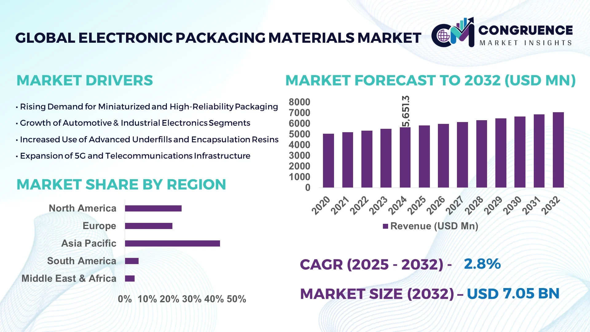
The Global Electronic Packaging Materials Market was valued at USD 5,651.3 Million in 2024 and is anticipated to reach a value of USD 7,048.4 Million by 2032 expanding at a CAGR of 2.8% between 2025 and 2032.
In 2025, Japan leads the global Electronic Packaging Materials Market due to its exceptional manufacturing infrastructure and continuous investment in semiconductor-related innovations. The country boasts advanced production capacity in high-purity materials used in semiconductor and microelectronic packaging, alongside strong support for R&D across photonics and thermal interface technologies.
The Electronic Packaging Materials Market serves several core sectors including consumer electronics, automotive electronics, telecommunications, and industrial automation. Semiconductor packaging continues to represent a major share, driven by the miniaturization of devices and the integration of advanced functionality into compact systems. Recent innovations such as high thermal conductivity substrates, low-loss dielectric laminates, and halogen-free materials are addressing performance and environmental demands. Additionally, the increasing use of 5G devices and IoT-enabled applications is accelerating the consumption of specialized electronic packaging materials. Stringent environmental regulations, particularly in the European Union, are fostering demand for recyclable and lead-free materials. Meanwhile, North America is experiencing strong momentum due to rising investments in chip manufacturing and electric vehicles. Emerging economies in Southeast Asia are showing growing adoption fueled by industrial digitization and OEM manufacturing hubs. Future outlook remains positive with increased focus on hybrid material systems, enhanced power density packaging, and AI-driven material optimization techniques poised to reshape production strategies.
Artificial Intelligence is fundamentally reshaping the Electronic Packaging Materials Market by optimizing production processes, improving material design, and accelerating time-to-market. AI-enabled systems are increasingly used in precision quality inspection, which helps in the detection of micro-defects in laminates and substrates at a rate previously unattainable through manual or optical methods. AI-driven predictive maintenance tools are minimizing equipment downtime across packaging material manufacturing lines, increasing operational uptime by up to 22% based on recent factory automation benchmarks. Moreover, machine learning algorithms are assisting R&D departments in modeling thermal dissipation, electrical insulation, and material performance under dynamic stress conditions—cutting development cycles by over 35% in some leading labs.
Smart factories are integrating AI to adjust packaging material formulations in real-time, enabling greater material customization while maintaining uniformity and compliance with evolving regulatory standards. In supply chain operations, AI is streamlining inventory control and raw material forecasting, significantly reducing excess storage and procurement costs. As demand for high-performance packaging materials rises in electric vehicles and high-frequency telecom devices, AI’s role in ensuring material reliability and sustainability has become indispensable. The Electronic Packaging Materials Market is now transitioning into a data-centric ecosystem where AI delivers tangible, scalable advantages to both manufacturers and end-users.
"In April 2025, a major Japanese electronics manufacturer deployed an AI-powered inline inspection system for epoxy molding compounds used in semiconductor packaging, achieving a 38% reduction in defect rates and improving production throughput by 27% within six months of implementation."
The Electronic Packaging Materials Market is undergoing a significant transformation driven by technological advancements, increased electronics consumption, and evolving regulatory frameworks. Rapid innovation in chip design and device miniaturization is spurring demand for thermally stable, high-insulation materials. The market is influenced by global trade dynamics, environmental compliance requirements, and the emergence of next-generation applications such as AI processors and quantum computing. With the proliferation of consumer electronics, electric vehicles, and smart infrastructure, manufacturers are investing in materials that offer superior performance and sustainability. In parallel, global initiatives aimed at reducing electronic waste are further shaping material innovation and lifecycle management in the Electronic Packaging Materials Market.
The rapid evolution of semiconductor devices, particularly in high-performance computing and power electronics, is significantly boosting the demand for advanced packaging materials. New chip architectures such as 3D-ICs, chiplets, and fan-out wafer-level packaging require high-purity materials with enhanced thermal and dielectric properties. These advancements necessitate the use of novel substrates, adhesives, and encapsulants that can support greater integration and functionality without compromising reliability. For example, low-k dielectrics and lead-free solder balls are being widely adopted to enhance signal speed and reduce power consumption. This technological push is reinforcing the need for consistent innovation across the Electronic Packaging Materials Market, especially among R&D-intensive manufacturers.
The Electronic Packaging Materials Market is facing increasing pressure from stringent environmental regulations, especially in developed markets such as the EU, Japan, and California. Compliance with directives like RoHS (Restriction of Hazardous Substances) and REACH (Registration, Evaluation, Authorisation and Restriction of Chemicals) is limiting the use of certain flame retardants and lead-based components. As manufacturers seek alternatives, the cost and time associated with reformulating materials and securing regulatory approvals have surged. This often delays product rollouts and complicates global supply chains. Additionally, testing and certifying new eco-friendly materials to meet both performance and environmental standards remains a significant operational challenge for industry stakeholders.
The accelerating growth of electric vehicles and advanced driver-assistance systems (ADAS) is creating new opportunities within the Electronic Packaging Materials Market. As automotive electronics evolve to support higher thermal loads and complex circuitry, demand is surging for heat-dissipating substrates, high-reliability encapsulants, and EMI shielding materials. For instance, EV battery management systems and onboard computing units require packaging materials capable of operating across wide temperature ranges and maintaining mechanical stability under vibration. In response, manufacturers are exploring ceramic-based materials and hybrid composites tailored for automotive applications. With countries tightening emission norms and promoting EV adoption, this sector is poised to become a critical growth engine.
Fluctuating prices and unpredictable availability of essential raw materials such as copper, silver, epoxy resins, and polyimides are posing significant challenges to the Electronic Packaging Materials Market. Geopolitical uncertainties, logistical disruptions, and export restrictions have further aggravated material procurement cycles. These supply chain bottlenecks result in inconsistent production schedules, higher input costs, and strained profit margins. Additionally, limited availability of high-purity materials hampers the scaling of advanced packaging technologies, particularly in regions lacking domestic sources. Manufacturers are increasingly pressured to diversify supply chains and invest in sustainable material alternatives to maintain competitiveness in this dynamic landscape.
Surge in Use of Lead-Free Solder Materials: Regulatory restrictions and environmental sustainability goals have accelerated the transition toward lead-free solder materials in the Electronic Packaging Materials Market. Tin-silver-copper (SAC) alloys are now preferred for their improved reliability and thermal performance. Major OEMs have reported a 45% year-over-year increase in lead-free solder consumption, particularly across telecom and computing sectors that demand long-term stability and compliance with international safety standards.
Integration of High-Performance Liquid Crystal Polymers (LCPs): Liquid crystal polymers are increasingly used in high-frequency electronic devices for their low dielectric constant and moisture resistance. In 2025, LCP usage in 5G modules and wearables rose significantly, with some manufacturers achieving a 28% improvement in device signal integrity. Their adoption is particularly prominent in Asia-Pacific where compact design and performance optimization are top priorities.
Rise in Modular and Prefabricated Construction: The adoption of modular construction is reshaping demand dynamics in the Electronic Packaging Materials Market. Pre-bent and cut elements are prefabricated off-site using automated machines, reducing labor needs and speeding project timelines. Demand for high-precision machines is rising, especially in Europe and North America, where construction efficiency is critical.
Adoption of AI-Optimized Material Formulations: AI-based tools are now guiding the selection and synthesis of electronic packaging materials based on application-specific performance criteria. In 2025, several major suppliers reported a 32% reduction in R&D time by leveraging AI simulation platforms to predict thermal conductivity, adhesion behavior, and dielectric properties. This trend is helping manufacturers tailor materials with unprecedented precision for high-growth sectors like autonomous vehicles and industrial automation.
The Electronic Packaging Materials Market is segmented into three major categories: by type, by application, and by end-user. Each of these segments contributes uniquely to the evolving structure of the market, driven by technological innovation and industry-specific demands. On the basis of type, materials such as substrate, encapsulation resin, bonding wire, and lead frame form the core components of the market. By application, segments include consumer electronics, automotive, industrial electronics, and telecommunications, among others. The market is also analyzed based on end-users such as OEMs, semiconductor manufacturers, and contract manufacturers. With rapid shifts in microelectronics, automotive electrification, and smart device proliferation, certain subsegments are emerging as innovation hotspots. Industry decision-makers are closely monitoring how advanced packaging types and emerging applications in high-frequency electronics are reshaping demand dynamics and supply chain strategies.
In the Electronic Packaging Materials Market, substrates represent the leading product type due to their critical role in providing mechanical support and electrical interconnectivity within electronic assemblies. High thermal conductivity and dimensional stability make substrates essential in both high-performance computing and power electronics. This dominance is driven by widespread adoption in multilayer PCBs and semiconductor packages used across consumer electronics and automotive systems.
The fastest-growing type is encapsulation resin, propelled by rising demand for durable and thermally stable protective materials in electric vehicles and 5G infrastructure. These resins offer superior moisture resistance and thermal insulation, which are vital for enhancing device reliability under harsh operating conditions. Advancements in low-halogen and halogen-free resin technologies are further accelerating their adoption across regulatory-sensitive regions.
Other types such as bonding wires and lead frames hold niche yet critical importance. Bonding wires—especially gold and copper variants—are widely used in IC interconnections, while lead frames continue to find applications in legacy packages and cost-sensitive markets, contributing to market diversity and resilience.
Consumer electronics remain the dominant application segment in the Electronic Packaging Materials Market, owing to high product turnover and consistent innovation in smartphones, wearables, laptops, and tablets. The miniaturization of components and demand for advanced features like high-resolution imaging, biometric sensors, and wireless connectivity have increased the need for high-performance packaging materials that ensure device efficiency and longevity.
Automotive electronics are currently the fastest-growing application, driven by the electrification of vehicles and the integration of safety, navigation, and infotainment systems. Materials used in these applications must withstand high thermal loads, vibration, and exposure to harsh environments. As EVs and hybrid vehicles expand globally, demand for thermally conductive and vibration-resistant packaging materials is rising significantly.
Other applications such as industrial electronics and telecommunications are gaining relevance as automation and high-speed communication technologies expand. These segments demand customized materials tailored for energy efficiency, signal integrity, and long-term durability, thereby supporting consistent innovation in packaging solutions.
Original Equipment Manufacturers (OEMs) lead the Electronic Packaging Materials Market in terms of end-user contribution. Their in-house production capabilities and focus on proprietary design and quality control make them the largest consumers of packaging materials. OEMs in sectors such as smartphones, automotive systems, and industrial controls require highly tailored solutions to meet performance, reliability, and regulatory standards.
The fastest-growing end-user segment is semiconductor manufacturers, particularly those investing in advanced chip packaging technologies like system-in-package (SiP), fan-out wafer-level packaging, and 3D stacking. As semiconductor companies expand their capabilities to meet next-generation computing and AI workloads, they demand innovative materials that can accommodate higher power densities and complex integration schemes.
Contract manufacturers, while smaller in scale, play a vital role in supporting rapid prototyping and high-volume production for global brands. Their ability to scale operations quickly and align with diverse client requirements ensures their continued relevance in shaping the supply landscape of the Electronic Packaging Materials Market.
Asia-Pacific accounted for the largest market share at 42.7% in 2024, however, North America is expected to register the fastest growth, expanding at a CAGR of 3.6% between 2025 and 2032.
The dominance of Asia-Pacific is attributed to its robust manufacturing infrastructure, high electronics output, and extensive presence of key semiconductor fabrication plants, especially in China, Japan, South Korea, and Taiwan. Meanwhile, North America's rapid growth is fueled by government-backed chip manufacturing investments, increased demand for electric vehicles, and rapid advancements in AI and industrial automation. Across all regions, electronic packaging materials are being reshaped by increasing demand for miniaturization, thermal management, and material sustainability, as global end-users seek performance-driven, cost-effective solutions in consumer electronics, automotive systems, and telecom infrastructure.
North America accounted for approximately 25.5% of the global Electronic Packaging Materials Market in 2024, supported primarily by the U.S. and Canada. Key industries such as automotive electronics, consumer electronics, and aerospace & defense continue to drive demand for advanced packaging materials, especially with the rising complexity of electronic components. U.S. government incentives under the CHIPS Act are fostering a resurgence in domestic semiconductor manufacturing, increasing demand for localized material sourcing. Additionally, smart manufacturing practices and AI integration are contributing to faster material design cycles and more efficient packaging processes. Regulatory emphasis on environmentally compliant materials is pushing adoption of halogen-free laminates and lead-free solder compounds, aligning with evolving EPA standards. The region is also witnessing significant growth in EV-related applications, where thermal conductivity and reliability of packaging materials are key to performance.
Europe captured around 21.3% of the global Electronic Packaging Materials Market in 2024, with Germany, France, and the UK emerging as the top contributors. The market is strongly supported by demand from the automotive and telecommunications sectors, as well as industrial automation. The region's push toward sustainability and stricter compliance with RoHS and REACH regulations have accelerated the shift to eco-friendly materials. Germany’s focus on electric mobility and the UK’s investments in green telecom networks have boosted regional consumption. Advanced material testing facilities and R&D programs funded by the European Commission are facilitating adoption of cutting-edge packaging solutions, particularly for low-loss and high-frequency electronic applications. Emerging technologies such as 5G infrastructure and AI chipsets are further shaping material innovation trends across the region.
The Asia-Pacific region commanded a leading 42.7% share of the global Electronic Packaging Materials Market in 2024, led by powerhouses such as China, Japan, South Korea, and Taiwan. These countries collectively account for the majority of global electronics and semiconductor production. China's rapid expansion of 5G infrastructure and India's increasing focus on domestic electronics manufacturing under national production-linked incentive schemes are driving demand for diverse packaging materials. Japan and South Korea continue to lead in the development and export of high-purity substrates and bonding materials. Regional innovation hubs like Shenzhen and Hsinchu are instrumental in facilitating new product development in AI processors, memory modules, and automotive microelectronics. Investments in advanced packaging technologies such as fan-out wafer-level packaging and 3D integration are accelerating material adoption across industries.
South America accounted for an estimated 6.2% of the global Electronic Packaging Materials Market in 2024, with Brazil and Argentina serving as the key regional contributors. Brazil’s growing domestic electronics manufacturing and expansion of the automotive electronics sector are driving material demand, particularly for encapsulants and heat-resistant substrates. In Argentina, infrastructure growth and smart grid deployments are fostering use of advanced electronics in the energy sector. Trade liberalization efforts and government-backed digital transformation initiatives are promoting cross-border investments in semiconductor packaging and related materials. While regulatory frameworks are still evolving, several countries in the region are offering tax incentives for local electronics production, supporting broader material procurement and development.
The Middle East & Africa region contributed approximately 4.3% to the global Electronic Packaging Materials Market in 2024. Countries such as the UAE and South Africa are at the forefront of adopting smart infrastructure and digital transformation strategies, which are propelling demand for electronic packaging components. In the UAE, national projects focused on AI-enabled systems and smart city deployments are creating demand for high-performance and thermally stable packaging materials. South Africa’s industrial electronics and construction sectors also contribute significantly, particularly through procurement of insulated and moisture-resistant substrates. Local governments are increasingly forming trade partnerships and technology transfer agreements to improve supply chain resilience. As these economies diversify beyond oil, investments in electronics and telecom infrastructure are expected to elevate regional demand further.
China – 31.2% Market Share
High production capacity and integrated semiconductor supply chains position China as the global leader in the Electronic Packaging Materials Market.
Japan – 14.5% Market Share
Strong end-user demand from consumer electronics and advanced material innovation ecosystems sustain Japan’s leadership in high-performance packaging materials.
The Electronic Packaging Materials Market features a competitive and fragmented landscape with over 80 active global and regional manufacturers. These players vary in size and specialization, ranging from established material science corporations to niche players focused on thermal interface materials or advanced encapsulants. The competition is largely shaped by innovation, strategic collaborations, and supply chain integration. Companies are investing heavily in research and development to advance material properties such as thermal conductivity, dielectric performance, and environmental compliance.
Strategic initiatives such as joint ventures, technology licensing agreements, and localized production units are being employed to improve regional reach and market responsiveness. Recent years have seen an uptick in mergers and acquisitions, particularly in Asia-Pacific and North America, as companies look to consolidate expertise and expand product portfolios. Many firms are adopting AI-driven material testing and digital twins to speed up product design and reduce development cycles. Additionally, supply chain resilience and compliance with evolving environmental regulations are emerging as key competitive differentiators.
Henkel AG & Co. KGaA
Hitachi Chemical Co., Ltd.
DuPont
Toray Industries, Inc.
BASF SE
Sumitomo Bakelite Co., Ltd.
Panasonic Holdings Corporation
Showa Denko Materials Co., Ltd.
Kyocera Corporation
Mitsui Chemicals, Inc.
NAMICS Corporation
Shin-Etsu Chemical Co., Ltd.
Technological innovation is a central driver in the evolution of the Electronic Packaging Materials Market. Advanced substrate technologies, such as low-loss, high-frequency compatible laminates, are now critical for 5G and high-speed computing applications. Liquid crystal polymers (LCPs) and modified polyimides are seeing rising usage due to their high thermal resistance and excellent electrical insulation properties. Encapsulation technologies have evolved with the introduction of low-halogen and halogen-free resins, meeting environmental regulations while ensuring mechanical durability.
One major area of advancement is AI-powered material optimization, where machine learning algorithms are used to simulate thermal and mechanical behavior under various operating conditions. This allows manufacturers to tailor materials with superior heat dissipation and lower dielectric constants. Flip-chip and wafer-level packaging techniques are driving demand for underfill materials and high-reliability solder pastes that can support ultra-miniaturized designs.
Nano-fillers and hybrid material systems are also gaining traction, improving thermal conductivity without compromising electrical performance. Furthermore, 3D printing and additive manufacturing of micro-packaging components are emerging, particularly for rapid prototyping in R&D labs. As electronics become more compact and powerful, the integration of smart materials with adaptive performance characteristics will define the next generation of packaging technologies.
• In March 2023, Sumitomo Bakelite announced the development of a new epoxy molding compound for high-power semiconductors with improved thermal cycling resistance, enabling extended performance for power modules used in electric vehicles.
• In September 2023, Henkel launched a low-void, high thermal conductivity die attach adhesive optimized for SiC devices, addressing the growing demand for efficient thermal management in EV powertrains and industrial inverters.
• In February 2024, Kyocera Corporation introduced an advanced ceramic substrate with improved thermal conductivity for use in 5G infrastructure, supporting higher operating frequencies and better signal performance.
• In June 2024, Toray Industries unveiled a next-generation flexible substrate material designed for foldable and wearable devices, featuring enhanced bending endurance and high-speed transmission performance.
The scope of the Electronic Packaging Materials Market Report encompasses a comprehensive analysis of the global landscape, covering key material types, diverse application domains, and regional performance metrics. The report segments the market into substrates, bonding wires, encapsulants, lead frames, underfills, and other specialized materials essential for electronic component packaging. It addresses their adoption across various applications including consumer electronics, automotive systems, industrial automation, telecommunications, and emerging 5G and AI applications.
Geographically, the report spans North America, Europe, Asia-Pacific, South America, and the Middle East & Africa, providing granular insights into production trends, consumption patterns, and regional innovations. Additionally, the report focuses on advanced manufacturing practices, including smart factory initiatives, digital twins, and the use of AI in material design. Emerging areas such as eco-friendly packaging, recyclable materials, and hybrid polymer-ceramic systems are covered to highlight sustainability-driven growth.
The competitive section highlights key global players, technological differentiators, and strategic developments shaping market positioning. Decision-makers will find in-depth analysis of regulatory influences, trade policies, innovation pipelines, and market entry strategies. This makes the report highly actionable for stakeholders planning product expansion, investment, or technology licensing in this dynamic industry.
| Report Attribute / Metric | Details |
|---|---|
| Market Revenue (2024) | USD 5,651.3 Million |
| Market Revenue (2032) | USD 7,048.4 Million |
| CAGR (2025–2032) | 2.8 % |
| Base Year | 2024 |
| Forecast Period | 2025–2032 |
| Historic Period | 2020–2024 |
| Segments Covered | |
| Key Report Deliverables | Revenue Forecast, Growth Drivers & Restraints, Technology Insights, Market Dynamics, Segmentation Analysis, Regional Insights, Competitive Landscape, Recent Developments |
| Regions Covered | North America, Europe, Asia‑Pacific, South America, Middle East & Africa |
| Key Players Analyzed | Henkel AG & Co. KGaA, Hitachi Chemical Co., Ltd., DuPont, Toray Industries, Inc., BASF SE, Sumitomo Bakelite Co., Ltd., Panasonic Holdings Corporation, Showa Denko Materials Co., Ltd., Kyocera Corporation, Mitsui Chemicals, Inc., NAMICS Corporation, Shin-Etsu Chemical Co., Ltd. |
| Customization & Pricing | Available on Request (10 % Customization is Free) |


