
Reports
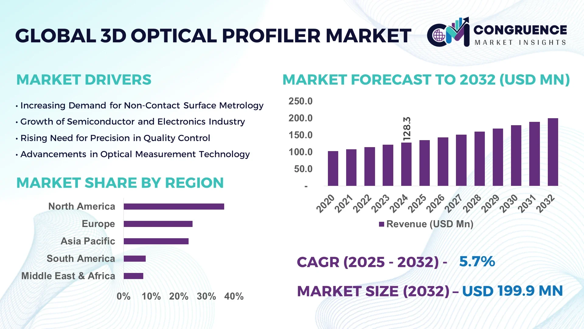
The Global 3D Optical Profiler Market was valued at USD 128.3 Million in 2024 and is anticipated to reach a value of USD 199.9 Million by 2032 expanding at a CAGR of 5.7% between 2025 and 2032.
The 3D Optical Profiler Market is gaining substantial traction globally as industries prioritize non-contact surface metrology solutions. These high-resolution measurement instruments are widely used in precision engineering, electronics, and semiconductor manufacturing for characterizing micro- and nano-scale surface features. Unlike traditional tactile methods, 3D optical profilers provide accurate topographic data without physical interaction, making them ideal for fragile materials and high-speed inspection lines. The market growth is further spurred by rising investments in quality control automation, emerging applications in MEMS fabrication, and stringent industrial compliance standards. Integration of software-driven analytics and AI-based image interpretation is also enhancing the measurement efficiency of 3D optical profilers globally.
AI is significantly transforming the 3D Optical Profiler Market by enabling smarter, faster, and more accurate surface inspection. Machine learning algorithms are now integrated with profiling systems to analyze surface topography in real time, identify defects with improved precision, and reduce false positives. AI-enhanced profilers can autonomously calibrate and adjust parameters to accommodate varying surface textures and environmental conditions, minimizing human intervention. In semiconductor and electronics sectors, AI-driven 3D optical profilers accelerate inspection throughput by detecting sub-micron irregularities that traditional techniques often miss. In medical device manufacturing, AI-enabled profilers contribute to verifying surface smoothness and coating thickness—critical to functionality and safety. Additionally, AI is empowering predictive maintenance of the profiler systems themselves, reducing downtime and increasing productivity. The convergence of AI with optical metrology not only enhances the accuracy of profiling but also lowers operational costs, making it a critical differentiator in competitive manufacturing industries.
"In February 2024, Bruker unveiled its AI-enhanced ContourX profiler, integrating real-time defect classification using deep learning, reducing inspection time by 30% across semiconductor lines."
The rising complexity in semiconductor devices has led to increased demand for non-contact metrology tools such as 3D optical profilers. As nodes shrink and wafer layers multiply, precise surface metrology becomes critical for maintaining yield and quality. Optical profilers offer unparalleled resolution and accuracy, essential for evaluating CMP processes, film thickness, and wafer flatness. Major semiconductor fabs across Asia and North America are incorporating these systems in their process lines to maintain nanometric tolerances and meet high-speed production requirements.
One of the significant restraints in the 3D Optical Profiler Market is the high upfront cost of advanced systems. These profilers often require significant capital investment for both hardware and software integration, making it difficult for small and mid-sized manufacturers to adopt. Additionally, training staff to operate and interpret the data from these high-end instruments adds to operational expenses. As the market continues to innovate, affordability remains a barrier, particularly in emerging economies and price-sensitive sectors like education and small-scale R&D labs.
The increasing use of advanced materials in automotive components and medical devices is creating opportunities for 3D optical profiler adoption. These industries require stringent surface quality checks, especially on parts like orthopedic implants, stents, and engine components. The non-destructive, highly detailed analysis provided by 3D optical profilers is ideal for ensuring product consistency and compliance with international standards. With rising investments in healthcare and automotive innovations, the demand for high-resolution, non-contact surface analysis tools is expected to grow significantly.
While 3D optical profilers deliver high-precision results, they also pose challenges related to system calibration and data interpretation. The complexity of analyzing high-resolution 3D images often requires expert-level knowledge and specialized software. Incorrect calibration can lead to inaccurate results, impacting the quality control process. Additionally, interpreting metrology data in multi-layered or highly reflective surfaces remains a technical hurdle, particularly in industries like optics and MEMS, where even minor discrepancies can lead to product failure.
The 3D Optical Profiler Market is witnessing a surge in innovation, particularly in terms of automation, precision, and AI integration. Manufacturers are focusing on developing profilers with faster scanning speeds and sub-nanometer vertical resolution to meet the demands of industries such as semiconductor, aerospace, and biomedical engineering. One major trend is the miniaturization of profiler systems for in-line production use, reducing footprint without sacrificing resolution. There is also a growing preference for white-light interferometry-based systems due to their ability to measure highly reflective and transparent surfaces. Optical profilers are now embedded with AI algorithms for real-time defect classification, enabling quicker decision-making in manufacturing processes. Additionally, cloud connectivity for remote diagnostics and monitoring is becoming common, supporting predictive maintenance and efficient data handling. These trends indicate a strong push toward smart, networked, and fully automated surface metrology systems that align with Industry 4.0 requirements.
The 3D Optical Profiler Market is segmented by type, application, and end-user, each playing a critical role in determining demand and innovation. By type, the market includes White Light Interferometry, Confocal Technology, and Focus Variation, among others, with each offering unique benefits in terms of speed, resolution, and material compatibility. By application, 3D optical profilers are used in Surface Topography, Step Height Measurement, and Roughness Analysis, supporting industries that demand non-destructive testing with sub-nanometer precision. End-user segments such as Semiconductors, Automotive, Aerospace, and Medical Devices are the primary adopters due to their reliance on high-precision surface inspection and quality assurance. The increasing complexity of components and growing emphasis on miniaturization are driving segment-specific advancements and adoption of 3D optical profiler systems globally.
White Light Interferometry: White Light Interferometry (WLI) remains the most widely adopted technology in the 3D optical profiler market. Known for its non-contact, high-resolution measurements, WLI is particularly effective in characterizing smooth surfaces such as silicon wafers and precision optics. It offers nanometer-level vertical resolution, making it ideal for applications that require extreme surface smoothness analysis. In 2024, WLI-based profilers accounted for more than 45% of the global market share, driven by their use in the semiconductor and display industries. These profilers also offer fast scanning speeds and compatibility with transparent or reflective surfaces, giving them a technical edge across several industries.
Confocal Technology: Confocal technology in 3D optical profiling is gaining momentum for its ability to provide sharp depth-of-field and high lateral resolution. Unlike WLI, confocal profilers excel in analyzing rough or uneven surfaces, making them ideal for components with complex geometries. Industries such as biomedical engineering and materials science utilize confocal profilers to study micro-impressions, coatings, and textured surfaces. In 2024, confocal systems captured approximately 30% of the market demand, especially in North America and Europe, where R&D and quality control labs prioritize multi-layered material analysis with precise z-axis data.
Focus Variation: Focus variation is another significant type of 3D optical profiling technology, ideal for analyzing steep slopes and rough surfaces like metal parts and cutting tools. This method combines image contrast data with vertical positioning, allowing fast, full-field topography mapping. In the automotive and tooling industries, focus variation profilers help ensure component uniformity and machining accuracy. In 2024, focus variation systems held around 15% of global market share and saw growing adoption in heavy-duty manufacturing environments. Their robustness and ability to handle large field-of-view samples make them indispensable in industrial production workflows.
Surface Topography: Surface topography analysis remains the most prominent application for 3D optical profilers. This process involves mapping the micro- and nano-scale contours of a material surface to detect irregularities, deformation, and quality inconsistencies. In 2024, this segment represented over 50% of the total application usage, driven by widespread adoption in semiconductor wafer inspections, lens manufacturing, and metal finishing. Optical profilers offer rapid, repeatable surface maps that are critical in high-precision engineering, where even microscopic deviations can lead to product failure or performance degradation.
Step Height Measurement: Step height measurement is a critical application in electronics and MEMS device fabrication. 3D optical profilers are extensively used to measure film deposition layers, etched trenches, and coating thickness across wafers and substrates. This application accounted for nearly 25% of market usage in 2024, with strong demand in Asia’s semiconductor industry. Profilers equipped with interferometry or confocal capabilities ensure high-speed and accurate detection of height differences across extremely small feature sizes, which is essential for yield improvement and defect analysis in advanced manufacturing.
Roughness Analysis: Roughness analysis is another crucial application where 3D optical profilers offer clear advantages over contact-based methods. This involves quantifying the average surface deviations and irregularities on parts used in medical implants, aerospace components, and tooling. In 2024, over 20% of profilers sold were used primarily for surface roughness measurements. Optical profilers provide faster, cleaner, and higher-resolution outputs compared to stylus profilometers, helping engineers validate material specifications, coating uniformity, and process consistency. This ensures better component lifespan, lower wear rates, and higher functional performance.
Semiconductors: The semiconductor industry is the dominant end-user of 3D optical profilers, using them extensively for wafer inspection, thin film measurement, and defect detection. As the industry transitions toward 3nm and smaller nodes, the requirement for ultra-precise, non-contact metrology tools has intensified. In 2024, semiconductor manufacturers contributed to nearly 40% of the total 3D optical profiler market. Profilers are embedded within production lines for in-situ quality control, reducing yield loss and ensuring process repeatability. Their role is vital in lithography, etching, and planarization stages, where surface integrity is critical.
Automotive: In the automotive sector, 3D optical profilers are increasingly used for inspecting engine parts, transmission components, and sensor housings. As vehicles become smarter and more electronic, the need for precise component surfaces has increased. In 2024, the automotive industry held around 20% of market demand. Profilers are used to ensure that coatings are applied uniformly, surfaces meet tight tolerance specifications, and tribological properties are maintained. With the shift toward electric vehicles, manufacturers are deploying profilers to validate battery casing surfaces and powertrain parts with nanometer accuracy.
Aerospace: The aerospace industry depends on 3D optical profilers for validating critical surface features in turbine blades, airframes, and composite materials. In 2024, the aerospace sector accounted for approximately 15% of end-user demand. Profilers help in maintaining compliance with airworthiness standards by analyzing fatigue cracks, wear surfaces, and aerodynamic contours. The ability to capture large area scans at high resolution makes these systems ideal for testing composite materials and metal alloys under stringent inspection protocols. This ensures component reliability under extreme flight conditions.
Medical Devices: Medical device manufacturing is a fast-growing end-user of 3D optical profilers, particularly in the production of implants, surgical instruments, and microfluidic devices. In 2024, over 10% of profilers sold were directed to the medical sector. These tools are used to inspect surface coatings, check for burrs or scratches, and ensure precise geometrical conformity. With increasing regulatory scrutiny, medical manufacturers rely on non-contact metrology to validate biocompatibility and functional safety of devices, ensuring compliance with ISO and FDA guidelines.
North America accounted for the largest market share at 36.4% in 2024; however, Asia-Pacific is expected to register the fastest growth, expanding at a CAGR of 7.2% between 2025 and 2032.
The regional performance of the 3D Optical Profiler Market is shaped by technology adoption, industrial output, and government-led manufacturing initiatives. North America's dominance stems from the early incorporation of optical profilers in semiconductor and aerospace sectors, while Asia-Pacific is benefiting from rapid industrialization, electronic exports, and a booming precision engineering sector. Europe remains a mature and innovation-driven market, and the Middle East & Africa is emerging gradually with investments in research hubs and advanced healthcare infrastructure.
Industrial Automation Driving Measurement Precision in North America
North America continues to dominate the global 3D optical profiler market due to robust investments in industrial automation, quality assurance, and microelectronics manufacturing. In 2024, the region held a 36.4% share, led by the U.S. which alone accounted for more than 80% of regional revenues. Semiconductors and aerospace industries remain top consumers of optical profilers, using them for wafer inspection, turbine blade surface analysis, and nanoscale defect detection. The presence of multiple metrology OEMs, tech startups, and advanced R&D centers fuels steady demand. Additionally, the push for onshore manufacturing and tight quality control standards contributes to the regional dominance in high-precision optical metrology tools.
Surface Metrology Gains Traction in European Automotive and Biomedical Sectors
Europe is a highly developed market for 3D optical profilers, driven by strict quality regulations and a strong emphasis on material science and research. In 2024, the region captured approximately 28.6% of the global market. Germany, the UK, and France are leading contributors, with widespread usage in automotive engine testing, aerospace composite inspection, and orthopedic implant manufacturing. European OEMs are investing in hybrid optical profilers that integrate white light interferometry with confocal scanning for complex surface analysis. Furthermore, the EU’s push for advanced manufacturing under “Industry 5.0” and increased medical device certifications have led to higher profiler deployments in production and regulatory environments.
Semiconductor Boom and Precision Manufacturing Propel Asia-Pacific Market
Asia-Pacific is emerging as the fastest-growing regional market for 3D optical profilers, expected to surpass 29.1% market share by 2032. In 2024, countries like China, Japan, South Korea, and Taiwan drove a combined 24.8% market share. The region's massive electronics and semiconductor manufacturing base heavily relies on 3D profilers for wafer-level metrology, MEMS inspection, and packaging validation. Governments across Asia-Pacific are backing domestic chip production, boosting profiler sales. Additionally, a strong automotive supply chain in Japan and precision equipment demand in South Korea support market expansion. The presence of local optical profiler manufacturers is also lowering hardware costs and increasing accessibility for mid-sized businesses.
Emerging Applications in Research and Medical Diagnostics Fuel Demand in MEA
The Middle East & Africa (MEA) region is still a niche market for 3D optical profilers, accounting for around 3.4% of global share in 2024. However, increasing funding for scientific research, nanotechnology, and modern healthcare is gradually elevating the market potential. Countries such as the UAE and South Africa are investing in advanced lab instrumentation for academic institutions, hospitals, and biomedical startups. Optical profilers are increasingly used in dental prosthetics, surface finishing of surgical tools, and microelectronics inspection. Collaborations with European and North American firms are also enhancing regional expertise and driving localized manufacturing of precision equipment.
The global 3D Optical Profiler market is characterized by intense competition among key players striving to enhance their technological capabilities and expand their market presence. Companies are focusing on strategic collaborations, product innovations, and regional expansions to gain a competitive edge. The market is witnessing a surge in demand for high-precision measurement tools across various industries, including automotive, aerospace, electronics, and healthcare. This demand is driving companies to invest in research and development to introduce advanced 3D optical profilers with improved accuracy and efficiency. Additionally, the integration of artificial intelligence and machine learning algorithms into these profilers is becoming a significant trend, enabling automated data analysis and enhancing measurement precision. The competitive landscape is further intensified by the entry of new players offering cost-effective solutions, compelling established companies to innovate continuously and maintain their market positions.
Zygo Corporation
Sensofar
KLA Corporation
Bruker Nano Surfaces
Taylor Hobson
Alicona Imaging GmbH
4D Technology
Cyber Technologies
Nanovea
Mahr GmbH
Zeta Instruments
AEP Technology
The 3D Optical Profiler market is undergoing significant technological advancements, driven by the need for precise and non-contact surface measurement solutions. One of the prominent technologies in this market is White Light Interference (WLI), which held a dominant position in 2023, capturing over 68.5% of the market share. WLI is favored for its versatility and ability to provide high-resolution, accurate measurements across a wide range of surface types. This technology is highly efficient in dealing with surface discontinuities and provides reliable data critical for quality control in manufacturing environments.
Another significant technology is Confocal Microscopy, which offers high-resolution imaging and depth selectivity, making it suitable for measuring complex surface structures. The integration of artificial intelligence (AI) and machine learning (ML) algorithms into 3D optical profilers is enhancing their capabilities, enabling automated data analysis, pattern recognition, and surface defect classification. These advancements are improving the accuracy and speed of surface measurements, expanding the application scope of 3D optical profilers across various industries.
Furthermore, the adoption of portable and handheld 3D optical profilers is on the rise, driven by the need for on-site surface inspection and field measurements. These devices offer flexibility and convenience, allowing for real-time quality control in various industrial settings. The focus on sustainability and green manufacturing practices is also influencing the development of eco-friendly 3D optical profilers with lower energy consumption and reduced environmental impact.
In February 2024, Zygo Corporation expanded its operations in India by hiring a dedicated sales and marketing team, aiming to provide enhanced support to local customers in the rapidly growing Indian manufacturing market.
In April 2022, Keyence Corporation announced the release of the VR-6000 3D Optical Profilometer, designed with a built-in motorized rotational unit, allowing users to take 3D measurements around their part's circumference without worrying about blind spots.
In 2021, Bruker Corporation launched light sheet microscopes, gaining popularity for their use in cancer diagnosis, assisting researchers in visualizing cancerous cells and tissues effectively.
ZYGO introduced the Nexview 650 system, providing 2D and 3D measurements with lateral sub-micron precision and vertical sub-nanometer accuracy, enhancing measurement capabilities for various applications.
The integration of AI and ML algorithms into 3D profiling systems has enhanced their capabilities, making them more efficient and user-friendly, leading to increased adoption across industries.
The 3D Optical Profiler market encompasses a wide range of applications across various industries, including automotive, aerospace, electronics, healthcare, and research. The market is driven by the increasing demand for high-precision, non-contact surface measurement solutions that offer accurate and reliable data for quality control and inspection processes. Technological advancements, such as the integration of AI and ML algorithms, are enhancing the capabilities of 3D optical profilers, enabling automated data analysis and improving measurement accuracy.
The market is segmented based on technology, application, end-user, and geography. Key technologies include White Light Interference and Confocal Microscopy, each offering unique advantages for different measurement requirements. Applications span across electronics and semiconductors, MEMS industry, automotive and aerospace, life sciences, and others. End-users range from large manufacturing enterprises to research institutions and healthcare facilities.
Geographically, the market is analyzed across North America, Europe, Asia-Pacific, Latin America, and the Middle East & Africa. North America holds a significant market share, driven by the presence of key players and advanced manufacturing industries. Asia-Pacific is anticipated to witness the highest growth rate, attributed to rapid industrialization and increasing adoption of advanced manufacturing technologies in countries like China and India.
The report provides an in-depth analysis of market trends, growth drivers, challenges, and opportunities, offering valuable insights for stakeholders to make informed decisions and strategize for future growth.
| Report Attribute/Metric | Report Details |
|---|---|
|
Market Revenue in 2024 |
USD 128.3 Million |
|
Market Revenue in 2032 |
USD 199.9 Million |
|
CAGR (2025 - 2032) |
5.7% |
|
Base Year |
2024 |
|
Forecast Period |
2025 - 2032 |
|
Historic Period |
2020 - 2024 |
|
Segments Covered |
By Type
By Application
By End-User
|
|
Key Report Deliverable |
Revenue Forecast, Growth Trends, Market Dynamics, Segmental Overview, Regional and Country-wise Analysis, Competition Landscape |
|
Region Covered |
North America, Europe, Asia-Pacific, South America, Middle East, Africa |
|
Key Players Analyzed |
Zygo Corporation, Sensofar, KLA Corporation, Bruker Nano Surfaces, Taylor Hobson, Alicona Imaging GmbH, 4D Technology, Cyber Technologies, Nanovea, Mahr GmbH, Zeta Instruments, AEP Technology |
|
Customization & Pricing |
Available on Request (10% Customization is Free) |


