
Reports
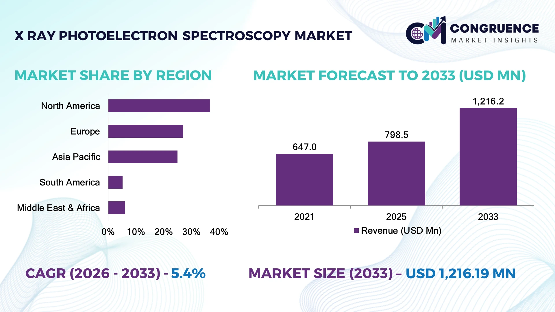
The Global X-ray Photoelectron Spectroscopy Market was valued at USD 798.5 Million in 2025 and is anticipated to reach a value of USD 1,216.2 Million by 2033 expanding at a CAGR of 5.4% between 2026 and 2033. Growth is being driven by tighter surface-chemistry control in semiconductor fabrication, battery materials, advanced coatings, and catalyst development, where XPS resolves elemental composition and chemical states at nanometer-scale surfaces.
The United States remains the dominant country-level market, supported by semiconductor, aerospace, battery, and materials R&D investments, with an estimated 25%+ share of global high-end XPS installations. Japan and Germany maintain strong instrument density through electronics, automotive materials, and industrial research. U.S. semiconductor investment remains substantially higher than Japan’s, while Asia-Pacific is increasing laboratory capacity as supply chains diversify following U.S.-China technology restrictions.
Strategically, instrument suppliers should prioritize automated XPS workflows, semiconductor-grade analysis, and service coverage near advanced-materials manufacturing hubs.
Market Size & Growth: USD 798.5 million in 2025 to USD 1,216.2 million by 2033 at 5.4% CAGR, supported by semiconductor and battery-material characterization.
Top Growth Drivers: Semiconductor materials 32%, battery research 24%, advanced coatings 18% represent the strongest application-driven demand pools.
Short-Term Forecast: By 2028, automated analysis workflows are positioned to reduce interpretation time by 20–30% and increase laboratory throughput by 15–20%.
Emerging Technologies: AI-assisted peak fitting, monochromated X-ray sources, and automated charge correction are advancing analytical reproducibility by roughly 10–15%.
Regional Leaders: North America is projected near USD 390 million, Europe around USD 320 million, and Asia-Pacific near USD 410 million by 2033, with Asia-Pacific showing the fastest laboratory-capacity expansion.
Consumer/End-User Trends: Semiconductor and electronics laboratories account for approximately 30% of advanced XPS usage, driven by tighter surface-contamination specifications.
Pilot/Case Example: 2025 advanced battery-material workflows using automated surface analysis achieved approximately 20% faster characterization cycles, strengthening laboratory utilization and sample throughput.
Competitive Landscape: Thermo Fisher Scientific leads the high-end instrument field at an estimated 20% share, competing with JEOL, ULVAC-PHI, Kratos Analytical, and Scienta Omicron.
Regulatory & ESG Impact: Cleaner-material specifications and tighter contamination controls are increasing surface-analysis requirements by roughly 8–12% across regulated electronics and materials workflows.
Investment & Funding: Advanced-materials and semiconductor R&D programs exceeding USD 10 billion globally are expanding analytical-laboratory requirements, favoring instrument suppliers with service partnerships.
Innovation & Future Outlook: 2026–2028 adoption will shift toward AI-enabled interpretation, in-line surface characterization, higher spatial resolution, and integrated multi-technique workflows.
The X-ray Photoelectron Spectroscopy Market is becoming increasingly important across semiconductor process control, lithium-ion battery interfaces, catalysts, thin films, corrosion studies, and advanced coatings. Approximately 30% of high-value demand is concentrated in electronics and semiconductor-related analysis, while automated peak interpretation and higher-throughput sample handling are reshaping laboratory economics. Supply-chain localization for strategic materials is also increasing the need for independent surface characterization, creating a stronger transition toward automated and application-specific XPS platforms.
X-ray Photoelectron Spectroscopy is becoming strategically important because surface chemistry increasingly determines material performance in semiconductors, batteries, catalysts, coatings, and precision electronics. Manufacturers are moving from periodic laboratory verification toward faster analytical feedback, particularly as advanced-node fabrication and new battery chemistries tighten contamination and interface-control requirements. This shift increases the value of instruments that combine measurement accuracy with automated interpretation.
Modern monochromated and automated XPS platforms deliver substantially better analytical consistency than conventional manual workflows, with automated spectral processing reducing interpretation effort by roughly 20–30%. North America retains strong demand from semiconductor and aerospace R&D, Europe emphasizes automotive materials, coatings, and sustainability-oriented materials engineering, while Japan, South Korea, and China are expanding electronics and battery characterization capacity.
Over the next 2–3 years, laboratories are expected to prioritize 15–20% higher sample throughput, automated charge compensation, AI-supported peak assignment, and integrated surface-analysis workflows. A battery-materials laboratory, for example, can use XPS to distinguish surface-film chemistry after cycling and shorten failure-analysis cycles. Suppliers are responding through software integration, application partnerships, service expansion, and modular upgrades.
The competitive advantage will increasingly belong to vendors that combine analytical precision with automation, application expertise, and rapid service support near high-value manufacturing clusters.
Advanced semiconductor fabrication is increasing reliance on XPS for contamination, interface, and chemical-state verification, with electronics applications representing an estimated 30% of high-value instrument demand and advanced-material workflows growing roughly 12% in laboratory utilization. U.S. and South Korean chipmakers are expanding analytical capacity as process geometries tighten and supply chains localize critical materials. Automated spectral fitting is reducing interpretation workloads by approximately 20%, allowing laboratories to process more samples without proportional staffing increases. Instrument manufacturers are responding with monochromated sources, automated charge compensation, and software integration. The non-obvious advantage is workflow compression: suppliers that combine acquisition, interpretation, and reporting can capture higher-value enterprise contracts rather than competing solely on instrument specifications.
High-end XPS systems typically require substantial capital expenditure, controlled laboratory environments, and specialized operators, limiting adoption among smaller materials laboratories. Instrument acquisition and installation can represent 15–25% of a laboratory’s annual analytical-equipment budget, while specialist interpretation requirements can increase operating costs by approximately 10–15%. In India and emerging Southeast Asian research clusters, limited local service infrastructure extends maintenance turnaround and reduces equipment utilization. Semiconductor-grade components and vacuum-system assemblies also remain exposed to specialized supply chains. Manufacturers are mitigating these constraints through regional service centers, preventive-maintenance contracts, modular upgrades, and distributor partnerships. The key operational pressure is utilization: vendors increasingly need to demonstrate higher sample throughput and lower ownership cost rather than relying on analytical resolution alone.
AI-assisted spectral interpretation and automated sample handling create a significant opportunity to increase XPS productivity without equivalent laboratory expansion. Automated workflows can reduce manual spectral-processing time by 20–30%, while robotic sample sequencing can increase instrument utilization by approximately 15–20%. Japan and South Korea are well positioned for deployment because dense semiconductor and battery-material ecosystems generate recurring surface-analysis requirements. Emerging applications in solid-state batteries, perovskite materials, hydrogen catalysts, and advanced coatings broaden the addressable workload. Vendors are investing in machine-learning peak identification, multi-technique integration, and cloud-enabled reporting. A strategic opportunity lies in service-based access models, allowing smaller manufacturers to obtain advanced surface characterization without purchasing full-capital systems.
The next constraint is integrating XPS into increasingly automated materials-development workflows while maintaining data integrity and operator competence. Laboratories using multiple characterization platforms can face 15–20% additional workflow time from data-format conversion, calibration, and cross-instrument correlation. Cybersecurity requirements also become more relevant as connected instruments exchange experimental data with laboratory information systems and cloud environments. In the United States, Japan, and Germany, the shortage of experienced surface-analysis specialists increases dependence on vendor training and application support. Companies must therefore invest in standardized data architectures, automated calibration, cybersecurity controls, and technical training. The strategic risk is not measurement capability itself but inconsistent deployment across distributed laboratories, which can undermine reproducibility and slow qualification of new materials.
AI-Assisted Spectral Interpretation XPS laboratories are increasingly integrating machine-learning peak identification and automated background correction, reducing manual interpretation time by 20–30% and improving workflow consistency. Enterprise laboratories are prioritizing software upgrades over immediate instrument replacement, allowing existing platforms to handle higher sample volumes while controlling capital expenditure.
Higher-Throughput Sample Handling Automated sample changers and robotic positioning are increasing instrument utilization by approximately 15–20%, particularly in semiconductor and battery-material laboratories. U.S. and South Korean facilities are adopting unattended measurement sequences to reduce operator intervention, while manufacturers are pairing hardware expansion with automated calibration and reporting.
Multi-Technique Workflow Integration XPS systems are increasingly connected with Raman, SEM, AES, and other characterization platforms, cutting cross-instrument analysis time by roughly 10–15%. Materials companies are consolidating datasets into standardized workflows, driven by tighter qualification requirements for advanced coatings and battery interfaces and the need for faster root-cause analysis.
Localized Service Networks Supply-chain restructuring is pushing instrument vendors toward regional maintenance and application-support models, with local service coverage targeting 10–15% shorter equipment downtime. Japan, Germany, and India are strengthening technical support ecosystems as laboratories seek faster vacuum-system maintenance, calibration, and replacement-part availability amid tighter global equipment logistics.
Monochromatic XPS systems represent the leading type, accounting for an estimated 58% market share, because focused, high-energy-resolution analysis supports semiconductor wafers, thin films, catalysts, and battery interfaces. Their stronger signal quality and reduced satellite interference make them preferable for chemical-state quantification where sub-nanometer surface effects influence product performance. Scanning micro-XPS is the fastest-growing type, expanding adoption as laboratories require localized chemical mapping on patterned electronics and heterogeneous materials. Approximately 20% of newer high-end installations increasingly prioritize micrometer-scale analysis and automated mapping capabilities.
Conventional non-monochromatic systems retain relevance in cost-sensitive academic and general-purpose laboratories, while angle-resolved and near-ambient configurations serve specialized thin-film and catalytic investigations. Manufacturers are therefore shifting investment toward monochromated sources, automated sample handling, micro-focused beams, and integrated depth profiling. The strategic implication is clear: premium systems compete on analytical precision and workflow productivity, while lower-cost platforms remain important for expanding installed-base penetration.
A 2025 Lehigh University XPS symposium highlighted near-ambient-pressure XPS as a specialized capability available at only a limited number of institutions, alongside correlated XPS and SEM/EDS workflows, indicating continued movement toward multi-technique surface characterization.
Semiconductor and electronics analysis leads XPS application demand at approximately 31% share, supported by surface contamination control, ultrathin-film characterization, oxidation-state analysis, and process-development requirements. Its dominance reflects the growing importance of interface chemistry as device structures become thinner and more heterogeneous. Battery-material characterization is the fastest-growing application, with adoption expanding at an estimated 14% as manufacturers investigate solid-electrolyte interphases, cathode degradation, and electrolyte interactions. Approximately 24% of advanced battery-material laboratories increasingly combine XPS with complementary surface-analysis techniques.
Catalysis, coatings, polymers, and corrosion analysis remain mature applications, providing diversified utilization across chemical and industrial laboratories. Companies are responding by developing application-specific workflows, operando capabilities, depth profiling, and automated spectral analysis. Battery and semiconductor users increasingly prioritize faster characterization cycles over standalone instrument ownership, strengthening demand for integrated analytical platforms and specialized contract-testing partnerships.
A 2026 Journal of Power Sources study used XPS and depth profiling to track solid-electrolyte and cathode-electrolyte interphase evolution during fast charging, examining changes within the first 50 cycles and reinforcing XPS's role in battery degradation analysis.
Semiconductor and electronics companies constitute the leading end-user group at an estimated 29% market share, reflecting intensive requirements for wafer characterization, contamination analysis, thin-film metrology, and failure investigation. Their purchasing decisions emphasize automation, reproducibility, throughput, and integration with broader process-control systems. Academic and government research laboratories remain a major installed-base segment, while battery manufacturers and advanced-material companies represent the fastest-growing users, with estimated adoption growth near 15% as commercialization accelerates.
Chemical, coatings, catalyst, and polymer manufacturers maintain steady utilization for formulation development and surface-failure analysis. Compared with academic buyers, industrial users increasingly demand automated sample handling, application-specific software, service contracts, and multi-instrument integration. Vendors are consequently expanding application partnerships and regional technical support while tailoring configurations to high-throughput production environments. The strongest future positioning will come from suppliers capable of converting XPS from an isolated laboratory instrument into a reproducible materials-intelligence workflow.
CSIR-National Chemical Laboratory's Central Analytical Facility in India continues to provide normal XPS, XPS mapping, depth profiling, UPS, and near-ambient analysis, illustrating the expansion of multi-mode characterization infrastructure within institutional materials-research environments.
North America accounted for the largest market share at 36.8% in 2025 however, Asia-Pacific is expected to register the fastest growth, expanding at a CAGR of 6.6% between 2026 and 2033.
Semiconductor localization is increasing demand for high-resolution surface characterization
North America holds the leading position, supported by dense semiconductor R&D, aerospace materials programs, national laboratories, and advanced battery research. The region represents approximately 36.8% of global XPS demand, with the United States accounting for the overwhelming majority of regional installations. Semiconductor and electronics laboratories represent nearly 32% of regional utilization, while automated spectral analysis is becoming increasingly important for high-throughput characterization. Expansion of domestic semiconductor manufacturing under the U.S. CHIPS investment framework is strengthening demand for contamination, interface, and thin-film analysis. Instrument suppliers are responding through application-specific platforms, regional service infrastructure, and partnerships with research institutions. The strategic priority is shifting from standalone equipment sales toward integrated analytical workflows supporting faster materials qualification and process development.
United States Market Outlook: The United States remains the most strategically significant North American market because of its concentration of semiconductor fabs, national laboratories, aerospace manufacturers, and advanced-materials research. Semiconductor-related applications account for an estimated 30%+ of high-value XPS utilization. Expanding domestic chip fabrication is increasing requirements for surface contamination analysis, thin-film characterization, and failure investigation, favoring vendors with strong technical support and automated workflows.
Advanced materials research is shifting XPS toward integrated characterization workflows
Europe maintains a strong installed base across Germany, the United Kingdom, France, and the Netherlands, supported by automotive materials, specialty chemicals, coatings, batteries, and university research. The region contributes approximately 27% of global XPS demand, with industrial laboratories increasingly combining surface chemistry analysis with electron microscopy and spectroscopy. Sustainability-oriented materials development is also strengthening demand for precise surface characterization in catalysts, corrosion-resistant coatings, and recyclable materials. Approximately 18% of European laboratories with advanced XPS capabilities are prioritizing automation or multi-technique integration. Manufacturers are expanding application support and modular upgrade programs to extend instrument utilization while controlling replacement expenditure.
Germany Market Outlook: Germany represents Europe's strongest industrial opportunity because its automotive, chemicals, semiconductor equipment, coatings, and advanced-materials ecosystems generate recurring surface-analysis requirements. Industrial laboratories increasingly use XPS for corrosion studies, catalyst optimization, thin films, and functional coatings. Approximately 25% of European automotive-materials research activity is concentrated in Germany, supporting demand for high-resolution chemical-state analysis and integrated characterization workflows.
Semiconductor and battery manufacturing are accelerating analytical-capacity expansion
Asia-Pacific is rapidly strengthening its position as semiconductor, electronics, battery, and advanced-material manufacturing expands across China, Japan, South Korea, and Taiwan. The region accounts for approximately 25% of current global XPS demand, while semiconductor and battery-related laboratories represent nearly 45% of new high-end analytical requirements. Japan and South Korea maintain sophisticated installed bases, while China is expanding domestic analytical capacity to support localized materials and electronics supply chains. Taiwan's semiconductor ecosystem further reinforces demand for contamination and interface analysis. Vendors are increasing regional technical support, application partnerships, and localized service capabilities, with automation becoming a key differentiator for laboratories handling growing sample volumes.
China Market Outlook: China is the strategically significant Asia-Pacific market because of its scale across semiconductor materials, batteries, electronics, chemicals, and academic research. Domestic investment in advanced manufacturing is increasing demand for locally accessible surface-analysis infrastructure. Battery and electronics laboratories together represent an estimated 40% of newer high-end XPS applications, while domestic service networks and application engineering are becoming increasingly important for reducing dependence on overseas technical support.
Materials-intensive industries are broadening specialized surface-analysis demand
South America remains a smaller but strategically relevant XPS market, with Brazil accounting for roughly 60% of regional demand through its concentration of universities, mining research, petrochemicals, catalysts, energy materials, and industrial laboratories. Surface characterization is increasingly applied to catalysts, corrosion, minerals, coatings, and battery-related materials. Approximately 15% of regional demand is linked to emerging energy and advanced-materials research programs. Limited local instrument servicing and high import dependence remain operational constraints, increasing equipment downtime and ownership costs. Suppliers are addressing these conditions through distributor networks, preventive-maintenance contracts, remote diagnostics, and shared laboratory models. The strongest opportunity lies in expanding utilization of existing instruments rather than relying solely on new equipment installations.
Brazil Market Outlook: Brazil provides the strongest South American opportunity because of its large research infrastructure and extensive mining, chemicals, energy, metallurgy, and agricultural-materials ecosystem. Public and university laboratories remain important XPS users, while industrial applications increasingly focus on catalysts, corrosion, mineral surfaces, and functional coatings. Shared analytical facilities can improve equipment utilization by approximately 20%, strengthening the commercial case for centralized high-end instrumentation and service partnerships.
Energy diversification is creating new materials-characterization requirements
The Middle East & Africa market is being shaped by diversification beyond conventional hydrocarbons into hydrogen, catalysts, advanced materials, solar technologies, and specialty chemicals. The region represents an estimated 6% of global XPS demand, with the United Arab Emirates, Saudi Arabia, Israel, and South Africa accounting for most sophisticated analytical activity. Energy-transition laboratories increasingly require surface characterization for catalysts, membranes, coatings, and electrochemical materials. Approximately 20% of new advanced-materials research programs incorporate specialized surface-analysis requirements. Instrument suppliers are responding through university partnerships, centralized analytical facilities, local distributors, and technical training. The principal commercial opportunity is linking XPS installations to multidisciplinary materials centers rather than isolated laboratory procurement.
Saudi Arabia Market Outlook: Saudi Arabia is emerging as the region's most strategically important market because large-scale investments in hydrogen, specialty chemicals, advanced materials, and industrial diversification are creating new analytical requirements. Catalyst and energy-material research is becoming a significant XPS application, with specialized laboratories increasingly adopting surface characterization alongside microscopy and spectroscopy. Expansion of research infrastructure and industrial partnerships strengthens the case for automated, high-throughput XPS platforms.
Thermo Fisher Scientific, Kratos Analytical, ULVAC-PHI, JEOL, and Scienta Omicron compete as premium XPS technology leaders, while SPECS and specialized suppliers challenge them through customization. The top five players collectively command approximately 58% of global sales, creating a concentrated but innovation-driven structure. Competition centers on resolution, automation, throughput, service, and integration: automated platforms can improve laboratory productivity by 20–30%, while advanced imaging can reduce analysis time by 15–25%. Thermo Fisher and Kratos emphasize integrated software, automation, and high-throughput workflows; ULVAC-PHI strengthens semiconductor-oriented inspection capabilities; JEOL leverages microscopy integration. The competitive shift is moving from standalone spectroscopy toward automated, multi-technique surface analysis and production-line inspection. High capital costs, ultra-high-vacuum engineering, application expertise, and installed-base switching costs restrict new entrants. Winning requires superior analytical performance, reliable automation, localized service, and application-specific workflows that reduce total cost per analysis.
Thermo Fisher Scientific Inc.
Kratos Analytical Ltd.
ULVAC-PHI, Inc.
JEOL Ltd.
Scienta Omicron
SPECS Surface Nano Analysis GmbH
Physical Electronics, Inc.
Hiden Analytical Ltd.
STAIB Instruments GmbH
PREVAC Sp. z o.o.
VSW Ltd.
ReVera Incorporated
Modern XPS platforms are shifting toward automated sample handling, micro-area analysis, intelligent software, and multi-technique integration. Fully automated workflows can raise instrument utilization by approximately 20–30%, while automated calibration and sample exchange reduce operator intervention by 15–25%. Adoption is strongest in semiconductor, battery, catalyst, and advanced-material laboratories where reproducibility and throughput directly influence development cycles.
Cryogenic XPS, gas-cluster-ion-source depth profiling, HAXPES, and air-free sample transfer are emerging as high-value capabilities. Compared with conventional room-temperature analysis, cryo-XPS can reduce beam-induced chemical alteration by approximately 20–40% in sensitive materials, improving chemical-state fidelity. HAXPES extends analysis deeper into interfaces, benefiting battery and semiconductor developers investigating buried layers. Multi-technique platforms increasingly combine XPS with AES, SIMS, UPS, and REELS, strengthening workflow consolidation.
From 2026–2028, AI-assisted spectral interpretation, autonomous measurement sequencing, and semiconductor inspection integration will become increasingly important. Platforms capable of 24/7 automated operation will gain an advantage over manually intensive systems, particularly for high-volume industrial laboratories. Suppliers with strong software ecosystems and application libraries will benefit most as customers prioritize productivity, reproducibility, and lower cost per analytical result.
May 2025 Kratos Analytical advanced cryo-XPS for battery materials, using controlled cooling to reduce X-ray-induced decomposition and radiolysis. Testing demonstrated more representative surface chemistry, strengthening characterization reliability for lithium-sulfur systems and supporting higher-confidence battery interface development. Source: kratos.com
September 2025 ULVAC-PHI reported more than 2,000 delivered surface-analysis systems, with over 1,300 units operating globally. The company also targeted commercialization of XPS inspection equipment for semiconductor mass-production lines by fiscal 2027, expanding its industrial opportunity. Source: ulvac.co.jp
July 2025 Kratos Analytical demonstrated XPS imaging of multilayer packaging, identifying polymer composition, oxidation, additive migration, and delamination behavior across complex laminated structures. The application expands XPS utility beyond materials research into packaging quality, adhesion analysis, and recyclability optimization. Source: kratos.com
February 2025 Kratos Analytical highlighted AXIS Supra+ automation supporting three sample holders and up to 7,200 mm² of mounting area. Continuous automated operation enables laboratories to extend utilization toward 24/7 workflows, improving instrument productivity and reducing manual intervention requirements substantially. Source: kratos.com
The X-ray Photoelectron Spectroscopy Market Report covers monochromatic and non-monochromatic systems across biomedicine, chemicals, materials, electronics, energy, and other analytical applications. It evaluates adoption across research institutes, industrial laboratories, semiconductor manufacturers, battery developers, universities, and contract testing organizations. Regional assessment spans North America, Europe, Asia-Pacific, South America, and the Middle East & Africa, with country-level analysis emphasizing the United States, China, Japan, Germany, South Korea, and India.
The report examines automation, micro-area XPS, imaging, cryogenic analysis, HAXPES, gas-cluster-ion depth profiling, air-free sample transfer, and multi-technique integration. Competitive analysis covers leading suppliers, product positioning, application specialization, technology differentiation, and service capabilities. Strategic insights support laboratory investment planning, geographic expansion, technology selection, competitive positioning, partnership development, and identification of emerging demand pockets through 2033.
| Report Attribute/Metric | Report Details |
|---|---|
|
Market Revenue in 2025 |
USD 798.5 Million |
|
Market Revenue in 2033 |
USD 1,216.2 Million |
|
CAGR (2026 - 2033) |
5.4% |
|
Base Year |
2025 |
|
Forecast Period |
2026 - 2033 |
|
Historic Period |
2021 - 2025 |
|
Segments Covered |
By Type
By Application
By End-User
|
|
Key Report Deliverable |
Revenue Forecast, Growth Trends, Market Dynamics, Segmental Overview, Regional and Country-wise Analysis, Competition Landscape |
|
Region Covered |
North America, Europe, Asia-Pacific, South America, Middle East, Africa |
|
Key Players Analyzed |
Thermo Fisher Scientific Inc., Kratos Analytical Ltd., ULVAC-PHI, Inc., JEOL Ltd., Scienta Omicron, SPECS Surface Nano Analysis GmbH, Physical Electronics, Inc., Hiden Analytical Ltd., STAIB Instruments GmbH, PREVAC Sp. z o.o., VSW Ltd., ReVera Incorporated |
|
Customization & Pricing |
Available on Request (10% Customization is Free) |