
Reports
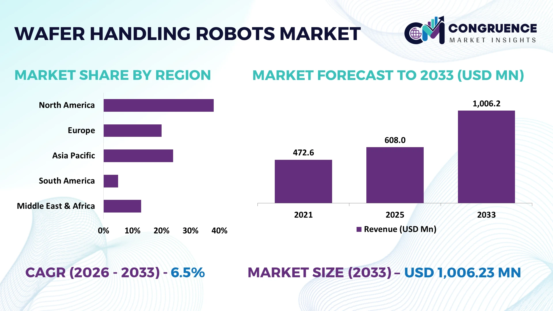
The Global Wafer Handling Robots Market was valued at USD 608 Million in 2025 and is anticipated to reach a value of USD 1006.23 Million by 2033 expanding at a CAGR of 6.5% between 2026 and 2033. Growth is driven by advanced semiconductor fabrication, 300 mm wafer automation, contamination-controlled robotic transfer, and expanding investments in AI processor and high-bandwidth memory manufacturing.
Taiwan represents a dominant country-level demand center for advanced wafer handling robots, supported by TSMC's semiconductor fabrication network and extensive advanced-node manufacturing capacity. TSMC accounted for approximately 70% of global pure-play foundry revenue in 2025, while advanced technologies at 7 nm and below represented 74% of its wafer revenue. South Korea provides a complementary demand base through Samsung Electronics and SK hynix, particularly in memory fabrication. US semiconductor export restrictions and fabrication localization initiatives are accelerating procurement diversification across major semiconductor manufacturing economies.
Robotics suppliers integrating vacuum-compatible transfer systems, precision motion control, and semiconductor equipment interfaces are positioned to secure long-term automation contracts with advanced fabrication facilities.
Market Size & Growth: USD 608 million in 2025, reaching USD 1,006.23 million by 2033 at 6.5% CAGR, driven by advanced semiconductor automation.
Top Growth Drivers: Advanced-node adoption reached 74% of TSMC wafer sales; global 300 mm equipment spending is projected to rise 31% in 2026; memory equipment spending increases 32%.
Short-Term Forecast: By 2028, installed 300 mm fabrication capacity is projected to expand approximately 8% annually, increasing robotic transfer requirements.
Emerging Technologies: AI motion optimization, dual-arm vacuum robots, and automated wafer alignment target 3 operational priorities: transfer precision, throughput, and contamination control.
Regional Leaders: Asia-Pacific dominates fabrication automation; North America expands advanced-node production; Europe strengthens semiconductor equipment engineering, supported by 3 distinct localization strategies.
Consumer/End-User Trends: Brooks Automation reports over 70,000 robots in active wafer production, demonstrating industrial-scale adoption of automated substrate handling.
Pilot/Case Example: TSMC's 2025 advanced-node production increased its 7 nm-and-below contribution by 5 percentage points, intensifying precision handling requirements.
Competitive Landscape: RORZE, Brooks Automation, DAIHEN, Yaskawa Electric, and Kawasaki Heavy Industries compete across 200 mm and 300 mm robotic platforms.
Regulatory & ESG Impact: ISO Class 1 cleanroom requirements influence robotic particle-control engineering; SEMI equipment standards strengthen operational compatibility.
Investment & Funding: Global 300 mm fabrication equipment spending is projected at USD 149 billion in 2026, supporting automation procurement.
Innovation & Future Outlook: Sub-2 nm fabrication, predictive maintenance, and integrated equipment front-end modules reshape robotic handling requirements through 2033.
The Wafer Handling Robots Market is increasingly shaped by semiconductor manufacturers prioritizing contamination-free transfer, precision alignment, and continuous fabrication equipment utilization. Vacuum-compatible robots, atmospheric transfer systems, and automated equipment front-end modules support lithography, deposition, etching, and metrology workflows. Brooks Automation reports more than 10,000 vacuum systems operating globally, demonstrating the established scale of automated wafer transportation. Emerging demand centers include advanced packaging facilities and compound semiconductor manufacturing, where substrate dimensions and handling requirements differ from conventional silicon fabrication. Semiconductor supply-chain localization is consequently reshaping robotics qualification, supplier partnerships, and equipment integration strategies across major manufacturing economies.
Wafer handling robots are becoming strategically important as semiconductor manufacturers increase automation intensity to support advanced logic, high-bandwidth memory, and contamination-sensitive fabrication processes. Semiconductor production is shifting toward geographically diversified manufacturing, supported by US CHIPS Act incentives and semiconductor investments in Japan. Taiwan maintains leadership in advanced foundry manufacturing, while South Korea concentrates on memory fabrication and the United States expands domestic leading-edge production. These developments strengthen demand for qualified robotic transfer systems, particularly across 300 mm wafer processing environments.
Technology differentiation increasingly depends on transfer precision, throughput, and particle control. Dual-arm wafer handling robots can theoretically improve transfer throughput by up to 100% over single-arm configurations under balanced operating conditions, although actual gains depend on equipment cycle times. Automated wafer alignment and vacuum-compatible motion control reduce handling variability during lithography, deposition, and etching operations. Manufacturers are integrating robotics with equipment front-end modules and standardized communication interfaces to simplify semiconductor tool qualification.
Between 2026 and 2028, semiconductor manufacturers will prioritize robotic platforms supporting 2 nm-class processing, predictive maintenance, and integrated equipment diagnostics. TSMC's Arizona fabrication expansion demonstrates how geographically distributed manufacturing creates opportunities for standardized automation platforms. Robotics suppliers investing in local technical support, precision engineering, and semiconductor equipment partnerships will strengthen customer retention and qualification advantages.
Increasing semiconductor process complexity is strengthening demand for precision wafer transfer automation. TSMC's advanced technologies, including 7 nm and below, accounted for 74% of wafer revenue in 2025, reflecting the concentration of production activity in sophisticated fabrication environments. Global semiconductor manufacturing equipment sales increased approximately 10% in 2024, while worldwide semiconductor sales expanded 19.1% during the same year. These developments increase requirements for contamination-controlled robotic handling, repeatable wafer positioning, and equipment uptime. US semiconductor manufacturing incentives are encouraging equipment suppliers to establish domestic engineering and technical support operations. RORZE, Brooks Automation, and DAIHEN are positioned to benefit through advanced motion-control platforms, vacuum robotics, and closer integration with semiconductor processing equipment manufacturers.
Wafer handling robot manufacturers face substantial cost pressure from specialized motion-control components, cleanroom-compatible materials, and semiconductor equipment qualification requirements. Global industrial robot installations declined approximately 3% in 2024, demonstrating uneven automation investment across manufacturing industries. Japan accounted for approximately 38% of worldwide industrial robot production, highlighting concentrated manufacturing capabilities and specialized component ecosystems. Semiconductor robots additionally require particle-controlled assemblies, vacuum-compatible bearings, and precision calibration, increasing production complexity compared with conventional industrial automation. US export controls on advanced semiconductor manufacturing equipment complicate cross-border technology procurement and customer qualification. Manufacturers are diversifying component suppliers, expanding local engineering operations, and standardizing robotic modules to reduce customization costs and protect delivery schedules.
Advanced semiconductor packaging creates opportunities for robotic systems capable of handling thinner wafers, temporary carriers, and increasingly complex substrate configurations. TSMC's advanced packaging capacity expansion supports chiplet integration and high-bandwidth memory assembly, while global semiconductor sales increased 19.1% in 2024. Advanced logic technologies accounted for 74% of TSMC's wafer revenue in 2025, strengthening the need for compatible handling systems across fabrication and packaging workflows. Robotic suppliers are developing low-vibration transfer mechanisms, adaptive end effectors, and machine-vision alignment for fragile substrates. Singapore and Malaysia provide additional manufacturing opportunities through established semiconductor assembly ecosystems. Suppliers combining wafer transfer robotics with advanced packaging equipment integration gain access to specialized applications beyond conventional front-end fabrication.
Advanced semiconductor manufacturing imposes increasingly demanding requirements for robotic positioning accuracy, contamination control, and equipment interoperability. Standard 300 mm silicon wafers provide approximately 125% more surface area than 200 mm wafers, increasing the potential production impact of handling defects. TSMC's advanced technologies represented 74% of wafer revenue in 2025, demonstrating the importance of reliable transfer systems in high-value processing environments. Integrating robots with equipment front-end modules, vacuum chambers, and factory automation software requires coordinated control protocols and extensive validation. South Korean memory manufacturers additionally face complex handling requirements across multilayer processing workflows. Robotics suppliers must invest in precision calibration, cybersecurity-compatible communication interfaces, and predictive diagnostics to maintain production consistency and reduce equipment qualification delays.
Dual-Arm Transfer Architectures Gain Preference: Semiconductor equipment manufacturers are integrating dual-arm wafer robots to improve chamber utilization and reduce transfer-related idle periods. A 300 mm wafer provides 125% more surface area than a 200 mm wafer, increasing the production value of each handling cycle. Dual-arm configurations enable 2 coordinated transfer paths, while independent blade control supports simultaneous wafer exchange. RORZE and Brooks Automation are refining motion sequences and end-effector designs to improve equipment throughput without expanding cleanroom footprints.
Vacuum Robotics Prioritize Particle Suppression: Advanced semiconductor processing increasingly requires robotic handling compatible with high-vacuum environments and contamination-sensitive surfaces. ISO Class 1 cleanroom conditions permit only 10 particles of 0.1 micrometers or larger per cubic meter. Vacuum transfer systems increasingly incorporate low-outgassing materials, magnetic coupling, and specialized bearings. DAIHEN and other automation suppliers are improving chamber-compatible robotic assemblies, helping equipment manufacturers control particle generation and reduce wafer contamination exposure during critical processing stages.
Modular Equipment Interfaces Simplify Qualification: Semiconductor equipment manufacturers are standardizing robotic communication, wafer mapping, and automated transfer interfaces across multiple fabrication platforms. SEMI E84 supports carrier handoff coordination, while SEMI E87 defines carrier management functions. Equipment front-end modules commonly accommodate 300 mm wafers within standardized handling environments. Robotics suppliers are developing modular controllers and interchangeable transfer assemblies, reducing integration complexity and supporting faster equipment configuration across geographically distributed semiconductor manufacturing facilities.
Predictive Diagnostics Reshape Robot Maintenance: Semiconductor fabs increasingly integrate motor-current monitoring, vibration analysis, and encoder feedback into robotic maintenance workflows. Advanced systems track 3 critical indicators: positioning deviation, drive-system condition, and transfer-cycle consistency. Taiwan's advanced fabrication facilities operate around continuous production schedules, making unscheduled handling interruptions particularly costly. Automation manufacturers are integrating diagnostic software with equipment controllers, allowing maintenance teams to identify developing mechanical faults before they disrupt wafer movement.
Atmospheric Wafer Robots represent a leading equipment category because they operate across equipment front-end modules, wafer loading stations, and cleanroom transfer interfaces. Their compatibility with standardized 200 mm and 300 mm wafer handling environments supports extensive deployment across semiconductor fabrication facilities. SCARA Robots remain widely applicable where compact installation footprints and repeatable horizontal movement are required, while Cartesian Robots support linear positioning tasks and specialized equipment layouts. Single-Arm Robots offer comparatively straightforward control architectures and lower mechanical complexity, making them suitable for equipment with moderate transfer frequency. Manufacturers are strengthening modular controller integration and automated wafer alignment to improve compatibility across processing platforms.
Vacuum Wafer Robots represent a strategically important high-performance category, particularly for etching, deposition, and other chamber-based semiconductor processes. Dual-Arm Robots are gaining attention where coordinated wafer exchange improves chamber utilization. A 300 mm wafer provides 125% more surface area than a 200 mm wafer, increasing the economic importance of contamination-free transfer. Suppliers including RORZE and DAIHEN are investing in low-particle mechanisms, compact robotic architectures, and application-specific motion control to strengthen equipment integration capabilities.
Wafer Transfer represents the central application for semiconductor handling robots because wafers repeatedly move between processing chambers, load locks, and equipment interfaces throughout fabrication. Standard 300 mm wafer platforms dominate advanced semiconductor manufacturing, supporting automated transfer systems with high positioning repeatability and contamination control. Wafer Loading and Unloading remains closely associated with equipment front-end modules and standardized carrier handling, while Wafer Sorting supports substrate classification, identification, and production routing. Inspection and Metrology requires controlled wafer positioning to protect measurement accuracy and minimize handling-induced defects. Equipment manufacturers are integrating robotic controllers with wafer mapping, alignment, and factory automation systems to improve processing consistency.
Etching and Deposition represent increasingly demanding robotic applications because vacuum chamber integration requires specialized materials, controlled motion, and reliable substrate exchange. Lithography similarly depends on precise wafer placement and contamination-sensitive transfer workflows. Advanced semiconductor technologies at 7 nm and below accounted for 74% of TSMC's wafer revenue in 2025, indicating substantial activity within highly sophisticated fabrication environments. Robotics suppliers are responding with vacuum-compatible platforms, improved motion calibration, and standardized chamber interfaces to support equipment reliability.
Semiconductor Foundries represent a leading end-user category because high-volume contract manufacturing requires extensive robotic integration across processing equipment and automated wafer transportation systems. Taiwan's manufacturing concentration, supported by TSMC and its supplier ecosystem, creates substantial demand for contamination-controlled handling technologies. Integrated Device Manufacturers maintain significant procurement requirements through vertically integrated semiconductor production, while Memory Manufacturers prioritize rapid wafer movement across repetitive deposition, etching, and inspection processes. Semiconductor Equipment Manufacturers represent another critical purchasing group because robotic subsystems are frequently integrated directly into processing tools before installation. Suppliers are strengthening engineering partnerships, qualification support, and standardized equipment interfaces to secure long-term integration agreements.
Advanced Packaging Facilities represent an emerging high-value customer category as heterogeneous integration introduces thinner substrates, temporary carriers, and specialized handling requirements. Research Laboratories require flexible robotic platforms for experimental processing, prototype development, and smaller production volumes. A 300 mm wafer offers approximately 2.25 times the surface area of a 200 mm wafer, increasing the value of reliable handling across advanced manufacturing environments. Robotics suppliers are developing interchangeable end effectors, configurable controllers, and specialized substrate handling systems to address increasingly differentiated customer requirements.
The Semiconductor Industry Association reported that worldwide semiconductor sales increased 19.1% in 2024, while its 2025 industry outlook emphasized continued investment in advanced manufacturing. These developments support sustained automation requirements among foundries, memory producers, and semiconductor equipment manufacturers.
Asia-Pacific accounted for the largest market share at approximately 65% in 2025 however, North America is expected to register the fastest growth, expanding at a CAGR of approximately 8.2% between 2026 and 2033.
Domestic Semiconductor Fabrication and Automation Localization
North America's wafer handling robots market is undergoing structural transformation through semiconductor manufacturing localization, advanced fabrication investments, and equipment supply-chain diversification. The United States dominates regional demand through semiconductor equipment manufacturers, integrated device manufacturers, and expanding foundry operations. The US CHIPS and Science Act provides approximately USD 52.7 billion for semiconductor manufacturing, research, and workforce development, strengthening the industrial foundation for precision automation. Arizona, Texas, and New York are emerging as important semiconductor manufacturing clusters requiring atmospheric wafer transfer, vacuum robotics, and automated equipment front-end modules. Canada contributes specialized semiconductor research, equipment engineering, and photonics manufacturing capabilities. Robotics suppliers are strengthening domestic technical support, equipment qualification services, and partnerships with fabrication equipment manufacturers. Regional competitiveness increasingly depends on contamination-control performance, rapid commissioning, and compatibility with advanced semiconductor manufacturing platforms.
United States Market Outlook: The United States is strengthening its semiconductor manufacturing position through TSMC's Arizona operations, Intel's domestic fabrication network, and Micron's memory manufacturing investments. TSMC's Arizona facility began commercial production using 4 nm technology in 2024. These advanced manufacturing capabilities require high-precision wafer transfer, automated substrate alignment, and vacuum-compatible robotic handling systems. Equipment suppliers are expanding local integration capabilities to support semiconductor production continuity.
Semiconductor Equipment Engineering and Precision Automation Integration
Europe's wafer handling robots market benefits from established semiconductor equipment engineering, precision motion-control technologies, and specialized industrial automation capabilities. Germany, the Netherlands, France, and Italy represent important centers for semiconductor equipment development and advanced manufacturing. The European Chips Act aims to strengthen the European Union's global semiconductor market position toward 20% by 2030, encouraging manufacturing investment and equipment localization. ASML's semiconductor equipment ecosystem in the Netherlands supports sophisticated wafer positioning and automated substrate handling requirements, while German semiconductor manufacturers emphasize industrial, automotive, and power semiconductor production. European robotics suppliers focus on equipment interoperability, particle-controlled motion systems, and specialized handling architectures. Investment priorities increasingly favor advanced equipment integration, cleanroom-compatible components, and standardized automation interfaces that support manufacturing flexibility across semiconductor technology platforms.
Germany Market Outlook: Germany represents a strategic European semiconductor manufacturing center through Dresden's established fabrication ecosystem and automotive semiconductor specialization. Infineon Technologies is developing its Smart Power Fab in Dresden, supported by an investment of approximately EUR 5 billion. The facility strengthens demand for automated wafer handling, advanced substrate positioning, and integrated manufacturing equipment. German precision engineering capabilities support robotic component development and specialized equipment qualification.
Semiconductor Manufacturing Concentration and Robotics Production Leadership
Asia-Pacific dominates the wafer handling robots market through extensive semiconductor fabrication capacity, established robotics manufacturing ecosystems, and concentrated equipment procurement. Taiwan, South Korea, Japan, and China form the region's principal semiconductor automation centers. Taiwan specializes in advanced foundry manufacturing, South Korea emphasizes memory fabrication, and Japan maintains strong capabilities in precision robotics and semiconductor production equipment. China continues expanding domestic fabrication capacity and semiconductor equipment localization. The region accounted for more than 70% of global semiconductor manufacturing capacity in recent industry assessments, supporting substantial deployment of atmospheric and vacuum wafer handling robots. RORZE, DAIHEN, and other Japanese equipment suppliers benefit from proximity to semiconductor manufacturing customers and specialized component networks. Regional manufacturers are strengthening dual-arm robotic platforms, wafer alignment capabilities, and automated transfer systems to support increasingly complex production workflows.
Taiwan Market Outlook: Taiwan represents a leading demand center for advanced wafer handling automation through TSMC's fabrication network and its semiconductor equipment supplier ecosystem. TSMC's advanced technologies at 7 nm and below accounted for approximately 74% of wafer revenue in 2025. The concentration of sophisticated fabrication processes strengthens requirements for contamination-controlled transfer systems, high-precision positioning, and continuous equipment operation. Local engineering partnerships support faster robotic qualification and maintenance response.
Semiconductor Assembly Development and Research Automation Expansion
South America's wafer handling robots market remains concentrated in specialized semiconductor activities, research institutions, and limited domestic manufacturing operations. Brazil represents the principal regional semiconductor ecosystem, supported by electronics manufacturing, microelectronics research, and semiconductor design capabilities. The country's Nova Indústria Brasil industrial policy includes initiatives to strengthen domestic technological manufacturing and reduce dependence on imported electronic components. Argentina contributes university research and specialized electronics development, while Chile's technology ecosystem supports semiconductor-related research initiatives. Regional demand primarily involves laboratory-scale wafer transfer, equipment prototyping, and selected semiconductor production activities rather than extensive advanced-node fabrication. Imported robotic platforms face integration costs, specialized maintenance requirements, and limited local technical support availability. Suppliers are addressing these limitations through distribution partnerships, modular equipment configurations, and technical training arrangements.
Brazil Market Outlook: Brazil maintains the region's most developed semiconductor policy framework through the Brasil Semicon initiative, introduced in 2024 to strengthen domestic chip production and technology capabilities. The program supports investment incentives and semiconductor industrial development. Research organizations and specialized manufacturers represent important customers for wafer handling automation, particularly where equipment flexibility, localized maintenance, and compatibility with smaller production environments influence purchasing decisions.
Semiconductor Ecosystem Investment and Research Infrastructure Development
The Middle East & Africa wafer handling robots market is emerging through semiconductor research investment, electronics manufacturing diversification, and advanced technology infrastructure development. Israel maintains an established semiconductor ecosystem involving Intel, Tower Semiconductor, and specialized equipment technology companies. The United Arab Emirates is strengthening advanced technology research and industrial diversification, while Saudi Arabia is developing semiconductor-related capabilities through national technology initiatives. Israel's semiconductor manufacturing infrastructure includes Intel's Kiryat Gat fabrication operations, supporting requirements for precision equipment and automated substrate handling. Regional demand remains concentrated in established fabrication facilities and specialized research environments rather than widespread high-volume manufacturing. Equipment suppliers prioritize technical partnerships, application engineering, and specialized robotic integration. Long-term competitiveness depends on expanding semiconductor engineering expertise, qualified equipment maintenance networks, and access to advanced manufacturing technologies.
Israel Market Outlook: Israel represents the region's most established semiconductor manufacturing and engineering center, supported by Intel's fabrication operations and Tower Semiconductor's specialty foundry activities. Intel's Fab 28 in Kiryat Gat operates advanced semiconductor manufacturing infrastructure, creating demand for precision wafer handling and automated process integration. The country's semiconductor engineering workforce and equipment technology ecosystem strengthen opportunities for specialized robotic platforms and advanced manufacturing support services.
RORZE, Brooks Automation, DAIHEN, Yaskawa Electric, and Kawasaki Heavy Industries anchor the wafer handling robots market, with the top five suppliers collectively commanding an estimated 55% of industry activity through concentrated technical capabilities and established equipment qualifications. Competition bifurcates between Japanese precision automation specialists competing on vacuum robotics and chamber compatibility, and semiconductor automation integrators competing on equipment front-end module integration and contamination-controlled handling expertise. The basis of competition centers on positioning accuracy and particle-control performance rather than unit price: dual-arm systems deliver theoretical throughput improvements approaching 100% under balanced transfer conditions, while 300 mm platforms provide 125% greater processing surface area than 200 mm alternatives. Players compete through engineering partnerships with fabrication equipment manufacturers, modular controller development, and regional technical support expansion. Qualification complexity and precision component sourcing restrict new market entry.
RORZE Corporation
Brooks Automation
DAIHEN Corporation
Yaskawa Electric Corporation
Kawasaki Heavy Industries, Ltd.
JEL Corporation
Hirata Corporation
Genmark Automation
Robostar Co., Ltd.
Sanwa Engineering Corporation
Moog Inc.
Milara Inc.
Persimmon Technologies Corporation
Nidec Corporation
Current wafer handling technologies combine atmospheric SCARA robots, vacuum transfer mechanisms, precision encoders, and automated wafer alignment. Dual-arm configurations support simultaneous loading and unloading, offering up to 100% higher theoretical transfer capacity than single-arm systems when equipment cycles permit parallel operation. Advanced fabrication facilities predominantly process 300 mm wafers, requiring repeatable positioning, low particle generation, and reliable carrier interfaces. Manufacturers are integrating compact motion controllers with equipment front-end modules to improve throughput without increasing cleanroom floor space.
Emerging systems incorporate machine vision, predictive diagnostics, and adaptive trajectory planning. Optical wafer mapping identifies missing or misaligned substrates before transfer, while encoder feedback detects positioning deviations during operation. Automated monitoring replaces periodic manual inspection with continuous assessment of motor current, vibration, and transfer consistency. Robotics specialists supplying configurable controllers and diagnostic interfaces gain competitive advantages through shorter equipment qualification cycles and reduced maintenance intervention.
Between 2026 and 2028, intelligent robotics will increasingly support advanced packaging, thin-wafer handling, and digitally connected semiconductor production. Specialized end effectors accommodate fragile substrates, while vacuum-compatible materials reduce contamination risks. Suppliers investing in interoperable software, modular robot architectures, and localized technical support will strengthen customer retention as semiconductor manufacturers standardize automation across geographically distributed fabrication facilities.
December 2025: RORZE Corporation introduced its Flap Wrist technology at SEMICON Japan, featuring adjustable vacuum gripping for warped and thin wafers. The mechanism supports both conventional and advanced packaging substrates, including 3D chiplet integration, improving robotic handling flexibility. Source: rorze.com.
November 2025: AlixLabs installed Brooks Automation's Marathon 2 LEAP platform and MagnaTran vacuum robot for its 300 mm APS beta system. The integration doubles demonstration capacity and enables continuous automated wafer processing, strengthening commercial equipment qualification. Source: alixlabs.com.
October 2026: JEL Corporation opened its Onomichi factory, establishing its fifth manufacturing site in Japan. The expansion strengthens domestic production infrastructure for semiconductor wafer transfer robotics and supports manufacturing capacity diversification, equipment supply continuity, and customer servicing capabilities. Source: jel-robot.com.
June 2025: SEMI reported that advanced semiconductor fabrication capacity at 7 nm and below is projected to increase 69% by 2028. This expansion strengthens equipment manufacturers' requirements for precision wafer handling, automated transfer, and contamination-controlled robotics. Source: semi.org.
The Wafer Handling Robots Market Report evaluates semiconductor automation technologies, equipment configurations, and deployment requirements from 2026 through 2033. Type segmentation covers atmospheric, vacuum, single-arm, dual-arm, SCARA, and Cartesian robots. Application analysis examines wafer loading and unloading, transfer, sorting, lithography, etching, deposition, inspection, and metrology. End-user coverage includes semiconductor foundries, integrated device manufacturers, memory producers, equipment manufacturers, research laboratories, and advanced packaging facilities.
Regional assessment examines North America, Europe, Asia-Pacific, South America, and Middle East & Africa, emphasizing fabrication concentration, manufacturing localization, and equipment qualification. Technology analysis addresses 300 mm handling platforms, vacuum-compatible robotics, adaptive gripping, and predictive diagnostics. Competitive evaluation supports supplier selection, production investment, geographic expansion, and strategic positioning as semiconductor manufacturing becomes increasingly automated and technically specialized.
| Report Attribute/Metric | Report Details |
|---|---|
Market Revenue in 2025 | USD 608 Million |
Market Revenue in 2033 | USD 1006.23 Million |
CAGR (2026 - 2033) | 6.5% |
Base Year | 2025 |
Forecast Period | 2026 - 2033 |
Historic Period | 2021 - 2025 |
Segments Covered | By Type
By Application
By End-User
|
Key Report Deliverable | Revenue Forecast, Growth Trends, Market Dynamics, Segmental Overview, Regional and Country-wise Analysis, Competition Landscape |
Region Covered | North America, Europe, Asia-Pacific, South America, Middle East, Africa |
Key Players Analyzed | RORZE Corporation, Brooks Automation, DAIHEN Corporation, Yaskawa Electric Corporation, Kawasaki Heavy Industries, Ltd., JEL Corporation, Hirata Corporation, Genmark Automation, Robostar Co., Ltd., Sanwa Engineering Corporation, Moog Inc., Milara Inc., Persimmon Technologies Corporation, Nidec Corporation |
Customization & Pricing | Available on Request (10% Customization is Free) |