Reports
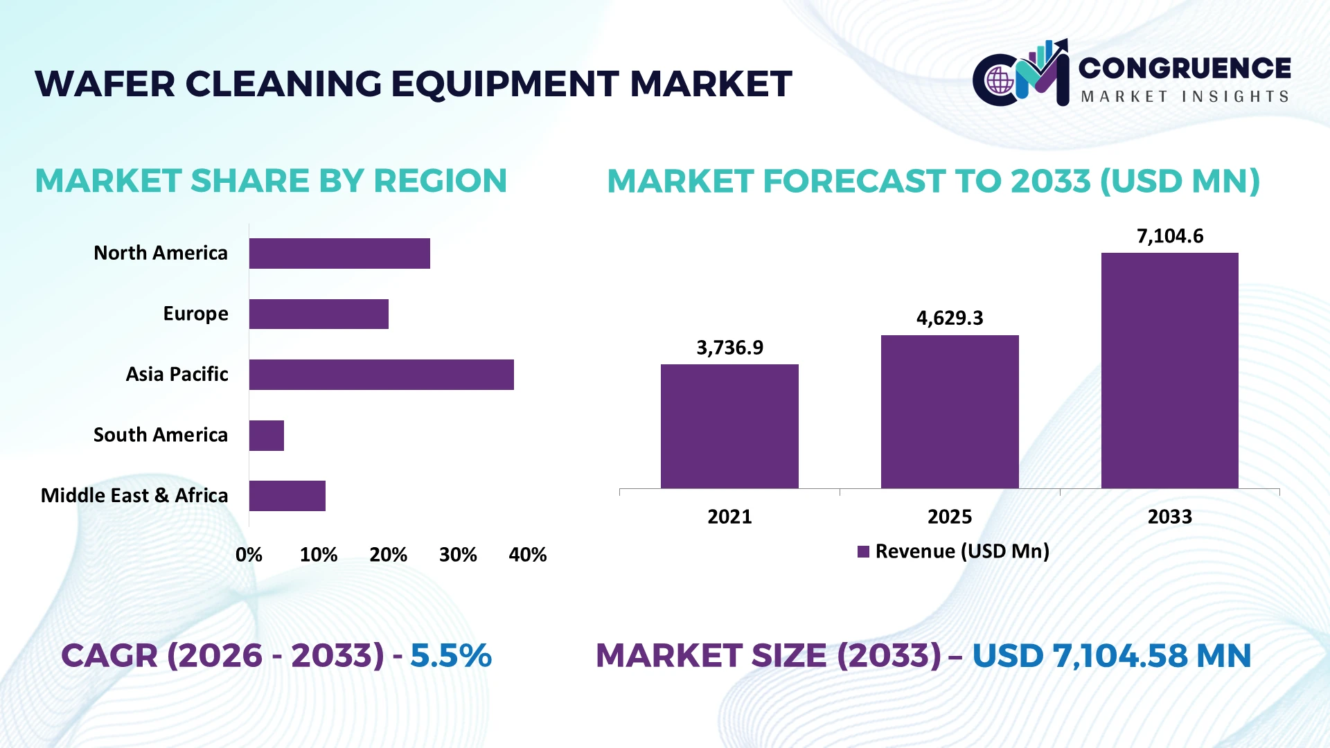
The Global Wafer Cleaning Equipment Market was valued at USD 4629.34 Million in 2025 and is anticipated to reach a value of USD 7104.58 Million by 2033 expanding at a CAGR of 5.5% between 2026 and 2033. Growing semiconductor fabrication capacity, advanced node production below 5 nm, rising demand for compound semiconductors, and tighter contamination control standards are accelerating investment in advanced wafer cleaning equipment across global chip manufacturing facilities.
Taiwan leads the global Wafer Cleaning Equipment Market with approximately 24% of worldwide semiconductor fabrication capacity, supported by continued investments in advanced foundries and high-volume logic manufacturing, while South Korea accounts for nearly 19% through memory chip expansion and next-generation process upgrades. The ongoing global semiconductor supply chain diversification following U.S.-China technology restrictions has increased localized equipment adoption, with automated wet cleaning utilization exceeding 70% in leading fabs, reinforcing competitive manufacturing resilience.
Strategic investment should prioritize regions expanding advanced semiconductor fabrication, where higher process complexity directly increases demand for precision wafer cleaning technologies.
Market Size & Growth: USD 4629.34 Million in 2025, projected to reach USD 7104.58 Million by 2033 at a CAGR of 5.5%, supported by advanced semiconductor fabrication expansion and stricter contamination control.
Top Growth Drivers: Advanced node production increased over 18%, silicon carbide wafer demand rose around 22%, and fab automation adoption exceeded 65%, strengthening equipment deployment.
Short-Term Forecast: By 2028, automated cleaning systems are expected to reduce chemical consumption by approximately 15% while improving process efficiency by nearly 12%.
Emerging Technologies: AI-enabled process monitoring, robotic wafer handling, and single-wafer cleaning technologies improve defect detection by about 20% and increase production consistency.
Regional Leaders: Asia Pacific exceeds USD 3800 Million, North America approaches USD 1500 Million, and Europe surpasses USD 900 Million by 2033, driven by domestic semiconductor expansion and supply chain localization.
Consumer/End-User Trends: More than 72% of advanced semiconductor fabs prioritize high-precision wet cleaning systems to improve yield and reduce particle contamination.
Pilot/Case Example: A 2026 advanced semiconductor manufacturing project achieved approximately 16% lower defect rates after integrating AI-assisted wafer cleaning optimization.
Competitive Landscape: Leading suppliers collectively control nearly 58% of the global market, with Tokyo Electron, SCREEN Semiconductor Solutions, Lam Research, Applied Materials, and SEMES maintaining strong competitive positions.
Regulatory & ESG Impact: New environmental compliance initiatives reduced ultrapure water consumption by nearly 14% through recycling technologies while supporting sustainable semiconductor manufacturing.
Investment & Funding: More than USD 12 Billion in semiconductor manufacturing expansion continues to support advanced wafer cleaning equipment through strategic partnerships and regional capacity additions.
Innovation & Future Outlook: Next-generation hybrid cleaning platforms, digital process control, and chemical optimization strengthen high-growth semiconductor manufacturing while supporting resilient global supply chain expansion.
Wafer Cleaning Equipment remains essential for maintaining high semiconductor yield as manufacturers transition toward smaller process nodes, compound semiconductor production, and automated fabrication environments. Recent innovations in AI-assisted process control and single-wafer cleaning have improved contamination removal efficiency by approximately 20%, while regional supply-chain localization and tighter environmental compliance continue influencing equipment procurement strategies, setting the foundation for broader strategic market evaluation.
Wafer cleaning equipment has become a strategic investment priority as semiconductor manufacturers pursue higher yields, advanced packaging, and localized fabrication capacity. Ongoing supply-chain restructuring driven by geopolitical technology restrictions is accelerating domestic fab development in the United States, Japan, and India, increasing demand for precision cleaning systems capable of supporting sub-5 nm production. Investment decisions increasingly favor platforms that improve process stability while reducing chemical and water consumption, strengthening both operational resilience and manufacturing competitiveness.
Single-wafer cleaning systems deliver approximately 18% lower chemical usage and nearly 15% higher particle removal efficiency than conventional batch cleaning technologies, making them increasingly attractive for advanced semiconductor nodes. Taiwan continues to lead high-volume deployment through mature foundry ecosystems, while the United States is expanding equipment adoption through new fabrication facilities focused on logic and specialty semiconductor production. Over the next two to three years, automated cleaning integration is expected to exceed 75% across newly commissioned advanced fabs, supported by digital process monitoring and predictive maintenance capabilities.
A recent fab modernization program integrating AI-assisted cleaning optimization reduced defect density by approximately 16% while shortening maintenance intervals. Equipment manufacturers are strengthening partnerships with semiconductor foundries, chemical suppliers, and automation specialists to deliver integrated process solutions. Companies establishing scalable, digitally connected cleaning platforms with sustainability-focused process optimization will secure stronger competitive positioning as semiconductor manufacturing complexity continues to increase.
Expansion of advanced semiconductor fabrication is reinforcing demand for high-precision wafer cleaning equipment as manufacturers target smaller process nodes and higher production yields. More than 70% of leading-edge fabs now utilize automated wet cleaning technologies, while contamination control requirements have tightened by nearly 20% for advanced logic production. Japan continues expanding specialty chemical manufacturing, strengthening equipment compatibility with next-generation cleaning processes. This combination of process complexity and localized semiconductor investment is prompting equipment suppliers to increase production capacity, establish technology partnerships, and introduce AI-enabled process control platforms. The strategic outcome is higher manufacturing consistency, lower defect density, and stronger long-term customer retention through integrated equipment ecosystems rather than standalone hardware sales.
The market continues to face structural pressure from rising costs of ultrapure chemicals, specialized components, and precision fluid management systems. Equipment manufacturing costs have increased by approximately 12%, while delivery timelines for critical semiconductor-grade components remain nearly 25% longer than historical averages. Dependence on highly specialized suppliers in Japan and South Korea creates procurement complexity for expanding fabrication projects. These constraints increase deployment costs and delay production schedules, particularly for emerging semiconductor manufacturers. Companies are responding through supplier diversification, localized component sourcing, long-term procurement agreements, and standardized equipment architectures that reduce dependence on single-source technologies while improving operational resilience and supply continuity.
Growing production of silicon carbide and gallium nitride devices is creating high-value opportunities for specialized wafer cleaning technologies optimized for advanced materials. Automated process optimization has improved cleaning cycle efficiency by approximately 17%, while AI-assisted inspection systems reduce contamination-related process variation by nearly 20%. India is expanding semiconductor manufacturing infrastructure through national electronics initiatives, opening opportunities for equipment suppliers entering new fabrication ecosystems. Leading manufacturers are increasing R&D investment, forming partnerships with specialty chemical providers, and developing modular cleaning platforms capable of supporting diverse wafer materials. This shift creates competitive differentiation through process flexibility rather than equipment scale alone, expanding opportunities across both advanced logic and power semiconductor manufacturing.
Integrating wafer cleaning equipment into highly automated semiconductor production environments remains a significant execution challenge. More than 60% of newly installed advanced manufacturing lines require customized software interfaces, while engineering integration can extend commissioning timelines by approximately 18%. Workforce shortages in semiconductor process engineering further slow deployment of intelligent cleaning platforms, particularly within new fabrication facilities. These operational complexities reduce implementation consistency and increase lifecycle support requirements. Equipment manufacturers must strengthen software interoperability, expand technical training partnerships, and invest in standardized digital communication protocols. Companies that simplify integration while maintaining high process precision will achieve stronger operational performance and sustain long-term competitiveness in increasingly automated semiconductor manufacturing environments.
AI-Driven Process Optimization Advanced fabs are embedding AI into wafer cleaning workflows, with automated parameter optimization improving particle detection accuracy by approximately 22% and reducing unplanned maintenance by nearly 18%. Taiwan and the United States are accelerating deployment as labor shortages and process complexity increase. Equipment suppliers are expanding software partnerships and integrating predictive analytics directly into cleaning platforms, enabling higher yield consistency and shorter qualification cycles.
Localized Equipment Manufacturing Expansion Semiconductor supply-chain restructuring is driving equipment localization, with domestic sourcing initiatives increasing by nearly 28% and localized component procurement improving by around 20% across new manufacturing projects. Japan and India are strengthening regional equipment ecosystems through supplier collaboration and manufacturing incentives. Companies are restructuring procurement networks, expanding regional service centers, and qualifying multiple component suppliers to improve delivery reliability and reduce operational disruption.
Resource-Efficient Cleaning Technologies Environmental compliance is accelerating adoption of low-chemical and water-efficient cleaning systems. Advanced recycling modules reduce ultrapure water consumption by approximately 16%, while optimized chemical dosing lowers process waste by nearly 14%. Semiconductor manufacturers are replacing legacy process modules with integrated sustainability-focused equipment. Equipment vendors are prioritizing closed-loop process designs and collaborative development with specialty chemical providers to improve compliance without sacrificing production throughput.
Hybrid Platform Standardization Multi-process cleaning platforms combining wet, dry, and plasma-assisted technologies are becoming standard across advanced manufacturing lines, reducing equipment footprint by approximately 15% and improving production flexibility by nearly 19%. South Korean memory manufacturers are adopting standardized modular architectures to accelerate product transitions. Suppliers are responding through modular platform development, interoperable software, and long-term integration partnerships that simplify fab upgrades while reducing lifecycle operating costs.
Single-Wafer cleaning represents the leading segment with approximately 42% of the market, supported by superior contamination control, compatibility with advanced process nodes, and seamless integration into highly automated fabrication lines. Individual wafer processing improves yield consistency and minimizes cross-contamination, making it the preferred solution for advanced logic and memory manufacturing. Wet Cleaning remains the largest process technology due to its effectiveness in removing particles and chemical residues, supporting more than 70% of mainstream semiconductor cleaning operations. Batch systems continue serving mature, high-volume production where lower processing costs remain a priority.
Dry Cleaning is the fastest-growing segment as manufacturers increase adoption for advanced materials, sensitive device architectures, and reduced chemical usage. Deployment has expanded by approximately 19% in advanced packaging and compound semiconductor production. Equipment suppliers are strengthening portfolios through modular platform development, plasma-assisted cleaning innovation, and collaborative technology programs that combine wet and dry capabilities. Investment priorities increasingly favor flexible systems capable of processing multiple wafer types while reducing operational complexity and supporting future semiconductor technology transitions.
Wafer Fabrication accounts for approximately 56% of total demand because every semiconductor production stage depends on high-purity surface preparation before deposition, lithography, and etching. Rising manufacturing complexity has increased cleaning frequency by nearly 18% in advanced production environments, making precision cleaning an essential operational requirement. MEMS Manufacturing maintains stable demand through sensor production, while Power Semiconductors continue expanding alongside electric vehicle, industrial automation, and renewable energy applications requiring specialized cleaning processes for silicon carbide and gallium nitride wafers.
Advanced Packaging is the fastest-growing application, with adoption increasing by approximately 21% as heterogeneous integration, chiplet architectures, and 3D packaging become mainstream manufacturing approaches. Equipment manufacturers are expanding automated cleaning capabilities, integrating advanced inspection technologies, and customizing systems for packaging-specific contamination control. Semiconductor producers are scaling dedicated packaging facilities and strengthening equipment partnerships, shifting investment toward cleaning platforms capable of supporting increasingly complex interconnect structures and high-density device assembly with consistent production quality.
Semiconductor Foundries represent approximately 48% of equipment demand due to continuous investment in high-volume production, advanced process nodes, and large-scale fabrication infrastructure. Their manufacturing intensity requires frequent equipment upgrades to maintain yield performance and contamination control. Integrated Device Manufacturers remain major purchasers through vertically integrated production strategies, while Research Institutes support pilot-scale innovation, process validation, and next-generation material development. Procurement decisions increasingly emphasize automation, interoperability, and long-term equipment service capability.
OSAT Companies are the fastest-growing end-user segment as advanced packaging expands across AI accelerators, high-performance computing, and automotive electronics. Equipment deployment has increased by approximately 20%, supported by growing packaging complexity and tighter cleanliness specifications. Vendors are responding through customized platform configurations, application-specific service agreements, and collaborative engineering programs with packaging providers. Competitive positioning increasingly depends on delivering scalable cleaning technologies optimized for both front-end fabrication and back-end semiconductor assembly, allowing suppliers to broaden customer relationships across the semiconductor value chain.
Asia-Pacific accounted for the largest market share at 61% in 2025 however, North America is expected to register the fastest growth, expanding at a 6.2% between 2026 and 2033.
Advanced Fab Expansion Accelerates Equipment Modernization
North America continues strengthening its position through rapid semiconductor manufacturing expansion, advanced fabrication investments, and increasing domestic equipment deployment. The region contributes approximately 20% of global wafer cleaning equipment demand, supported by new logic and memory fabrication facilities adopting automated contamination-control systems. More than 78% of newly installed production lines incorporate AI-enabled process monitoring integrated with precision cleaning platforms. Federal semiconductor manufacturing incentives and enterprise investments are accelerating equipment localization and supplier collaboration. Equipment vendors are expanding engineering support, digital service capabilities, and process optimization solutions to improve manufacturing yield while reducing production interruptions. Strategic partnerships between semiconductor manufacturers and equipment suppliers are shortening equipment qualification cycles and increasing operational resilience across advanced manufacturing facilities.
United States Market Outlook: The United States leads the regional market through extensive semiconductor fabrication expansion, advanced research infrastructure, and domestic equipment manufacturing capabilities. More than 80% of recently announced advanced fabrication projects include next-generation automated wafer cleaning technologies as part of integrated production planning. Companies continue investing in localized supply networks, digital manufacturing platforms, and long-term equipment partnerships, strengthening domestic semiconductor competitiveness while improving production flexibility for advanced logic, AI, and high-performance computing devices.
Sustainable Manufacturing Drives Process Innovation
Europe maintains a strong position through specialty semiconductor production, industrial automation, automotive electronics, and environmentally efficient manufacturing practices. The region accounts for approximately 15% of global equipment deployment, with increasing emphasis on chemical optimization and ultrapure water recycling. More than 65% of advanced semiconductor process upgrades now include resource-efficient cleaning technologies aligned with environmental compliance objectives. Collaborative research programs between equipment suppliers, semiconductor manufacturers, and research institutions continue accelerating precision process development. Companies are expanding modular equipment portfolios capable of meeting both sustainability requirements and advanced manufacturing performance targets while strengthening supply-chain resilience across industrial semiconductor production.
Germany Market Outlook: Germany remains the regional leader through its strong industrial electronics ecosystem, automotive semiconductor production, and advanced engineering capabilities. Semiconductor manufacturers continue modernizing fabrication facilities with intelligent cleaning systems capable of supporting increasingly complex production requirements. Automated process integration has expanded by approximately 18% across upgraded manufacturing lines, while collaboration between equipment developers and industrial technology companies strengthens domestic innovation and high-value manufacturing competitiveness.
Manufacturing Scale Reinforces Global Leadership
Asia-Pacific dominates global wafer cleaning equipment deployment through its concentration of semiconductor fabrication capacity, mature supply chains, and continuous investment in advanced manufacturing technologies. The region represents approximately 61% of global market demand, supported by extensive foundry, memory, and specialty semiconductor production. More than 75% of leading-edge semiconductor fabrication facilities operate highly automated precision cleaning platforms to maintain yield performance and contamination control. Strong manufacturing ecosystems across Taiwan, South Korea, Japan, China, and emerging semiconductor hubs continue driving equipment upgrades. Companies are expanding manufacturing capacity, strengthening regional supplier partnerships, and increasing localized engineering support to accelerate equipment deployment and reduce production lead times.
Taiwan Market Outlook: Taiwan remains the most strategically important national market due to its concentration of advanced semiconductor foundries and high-volume production infrastructure. Approximately one-quarter of global semiconductor fabrication capacity is located within the country, requiring continuous investment in precision wafer cleaning technologies. Equipment suppliers maintain dedicated engineering teams, application laboratories, and collaborative development programs with leading foundries to improve manufacturing efficiency, shorten process qualification, and support next-generation semiconductor production.
Industrial Electronics Support Emerging Demand
South America represents a developing market where semiconductor-related investments are primarily supported by industrial electronics, automotive manufacturing, and research-oriented semiconductor activities. The region contributes approximately 3% of global equipment demand while gradually expanding localized electronics manufacturing capabilities. Modernization initiatives have increased automation deployment by nearly 14% within selected manufacturing facilities. Infrastructure limitations and dependence on imported semiconductor equipment continue affecting implementation speed. Equipment providers are responding through regional distribution partnerships, technical support expansion, and localized maintenance capabilities that improve equipment availability while reducing operational downtime for industrial customers.
Brazil Market Outlook: Brazil leads regional demand through its industrial manufacturing base, electronics assembly operations, and expanding technology ecosystem. Manufacturers continue investing in automation upgrades supporting semiconductor-related production processes, particularly within industrial electronics applications. Equipment suppliers are strengthening local service capabilities and technical partnerships, enabling improved equipment utilization while supporting the country's gradual transition toward higher-value semiconductor manufacturing and research activities.
Technology Investment Supports Industrial Diversification
The Middle East & Africa market is advancing through industrial diversification strategies, technology infrastructure investments, and semiconductor ecosystem development initiatives. The region accounts for approximately 1% of global deployment while increasing investment in electronics manufacturing capabilities and research infrastructure. Smart manufacturing projects have expanded by nearly 16% across selected industrial zones, encouraging adoption of advanced process equipment. Governments and private enterprises are establishing technology partnerships to strengthen engineering capabilities, while equipment suppliers focus on training, technical services, and long-term industrial collaboration to support emerging semiconductor manufacturing ecosystems.
Saudi Arabia Market Outlook: Saudi Arabia is becoming the region's primary investment destination through industrial diversification programs, technology partnerships, and advanced manufacturing initiatives. Electronics manufacturing infrastructure continues expanding alongside national innovation strategies, creating opportunities for precision semiconductor equipment deployment. Equipment providers are establishing regional partnerships, workforce development programs, and engineering support capabilities to position themselves for long-term participation as semiconductor manufacturing capacity gradually develops.
The Wafer Cleaning Equipment Market is led by Applied Materials, Tokyo Electron, SCREEN Semiconductor Solutions, Lam Research, and SEMES, competing against specialized equipment innovators and regional process-equipment manufacturers. The top five companies collectively control approximately 58% of the market through broad product portfolios, integrated process technologies, and global customer support networks. Competition centers on contamination removal efficiency, automation capability, process uniformity, and lifecycle service rather than pricing alone. AI-enabled optimization improves equipment productivity by nearly 18%, while advanced chemical management reduces operating costs by approximately 15%, creating measurable competitive differentiation. Leading suppliers strengthen market positions through fabrication partnerships, localized manufacturing, vertical integration, and continuous platform innovation. Regional equipment providers compete by offering application-specific customization and faster engineering support for domestic semiconductor projects. High qualification requirements, process validation complexity, and customer switching costs remain significant entry barriers. Sustainable competitive advantage depends on precision engineering, digital integration, application expertise, responsive service infrastructure, and long-term collaboration with semiconductor manufacturers.
Applied Materials
Tokyo Electron Limited
Lam Research Corporation
SCREEN Semiconductor Solutions
SEMES
ACM Research
Shibaura Mechatronics Corporation
PSK Inc.
Modutek Corporation
Axus Technology
MEI Wet Processing Systems and Services
PVA TePla AG
JST Manufacturing
RENA Technologies GmbH
Advanced wet cleaning systems remain the foundation of semiconductor manufacturing, with single-wafer platforms deployed in nearly 75% of leading-edge fabrication lines. AI-assisted process control improves particle detection accuracy by approximately 18%, while automated chemical dosing reduces reagent consumption by around 15%. Integrated metrology enables real-time contamination monitoring, allowing manufacturers to stabilize yields and reduce rework across advanced logic, memory, and power semiconductor production.
Emerging technologies are shifting toward hybrid wet-dry cleaning, plasma-assisted surface preparation, ozone-based chemistries, and digital twin process optimization. Hybrid platforms improve cleaning uniformity by nearly 20% compared with conventional wet-only systems while lowering process cycle time by approximately 12%. Adoption of predictive maintenance has exceeded 55% across newly commissioned advanced fabs, enabling longer equipment uptime and faster qualification. Equipment suppliers increasingly integrate robotics, AI analytics, and closed-loop chemical management to strengthen process consistency while supporting stricter environmental compliance.
Between 2026 and 2028, autonomous cleaning platforms, machine-learning optimization, and advanced sensor integration will redefine competitive performance. Compared with legacy batch systems, intelligent single-wafer platforms deliver approximately 22% higher contamination removal efficiency while reducing operating costs by nearly 14%. Global technology leaders benefit through stronger customer retention, whereas specialized innovators gain opportunities in compound semiconductor and advanced packaging applications. Companies investing early in intelligent, modular, and sustainable cleaning technologies will secure superior operational flexibility and long-term manufacturing advantage.
May 2024 ACM Research introduced its Frame Wafer Cleaning Tool for advanced packaging with an integrated solvent reclamation system achieving nearly 100% solvent recovery, while completing first customer qualification with a major Chinese manufacturer, improving sustainability and packaging productivity.
November 2024 ACM Research announced a major upgrade to its Ultra C Tahoe cleaning platform, increasing throughput to more than 200 wafers per hour while reducing sulfuric acid consumption by up to 75%, strengthening cost efficiency for advanced-node semiconductor production.
July 2025 ACM Research enhanced its Ultra C wb Wet Bench Cleaning Tool with patent-pending nitrogen bubbling technology, improving wet etching uniformity for advanced-node manufacturing and strengthening process consistency for high-aspect-ratio semiconductor structures. Source: https://ir.acmr.com
May 2026 Applied Materials and SCREEN Semiconductor Solutions expanded their collaboration through the EPIC Center, integrating advanced wafer cleaning technologies into joint process development to accelerate commercialization of next-generation chips and improve manufacturing yield. Source: https://ir.appliedmaterials.com
The report delivers comprehensive analysis across Single-Wafer, Batch, Wet Cleaning, and Dry Cleaning technologies, evaluating their deployment patterns, operational efficiency, and technology adoption across semiconductor manufacturing. It assesses applications including Wafer Fabrication, MEMS Manufacturing, Power Semiconductors, and Advanced Packaging, alongside end-user analysis covering Semiconductor Foundries, Integrated Device Manufacturers, OSAT Companies, and Research Institutes. Regional assessment spans North America, Europe, Asia-Pacific, South America, and the Middle East & Africa, with strategic evaluation of manufacturing concentration, technology deployment, and supply-chain developments.
The study benchmarks more than 10 leading equipment manufacturers while examining automation adoption, AI-enabled process optimization, contamination-control technologies, and sustainability initiatives. It provides business-focused insights supporting investment prioritization, capacity expansion, partnership evaluation, competitive positioning, and product strategy between 2026 and 2033. The report also identifies emerging opportunities across compound semiconductors, advanced packaging, intelligent manufacturing, and digitally integrated wafer cleaning platforms, enabling stakeholders to align operational decisions with evolving semiconductor manufacturing requirements.
| Report Attribute/Metric | Report Details |
|---|---|
Market Revenue in 2025 | USD 4629.34 Million |
Market Revenue in 2033 | USD 7104.58 Million |
CAGR (2026 - 2033) | 5.5% |
Base Year | 2025 |
Forecast Period | 2026 - 2033 |
Historic Period | 2021 - 2025 |
Segments Covered | By Type
By Application
By End-User
|
Key Report Deliverable | Revenue Forecast, Growth Trends, Market Dynamics, Segmental Overview, Regional and Country-wise Analysis, Competition Landscape |
Region Covered | North America, Europe, Asia-Pacific, South America, Middle East, Africa |
Key Players Analyzed | Applied Materials, Tokyo Electron Limited, Lam Research Corporation, SCREEN Semiconductor Solutions, SEMES, ACM Research, Shibaura Mechatronics Corporation, PSK Inc., Modutek Corporation, Axus Technology, MEI Wet Processing Systems and Services, PVA TePla AG, JST Manufacturing, RENA Technologies GmbH |
Customization & Pricing | Available on Request (10% Customization is Free) |