
Reports
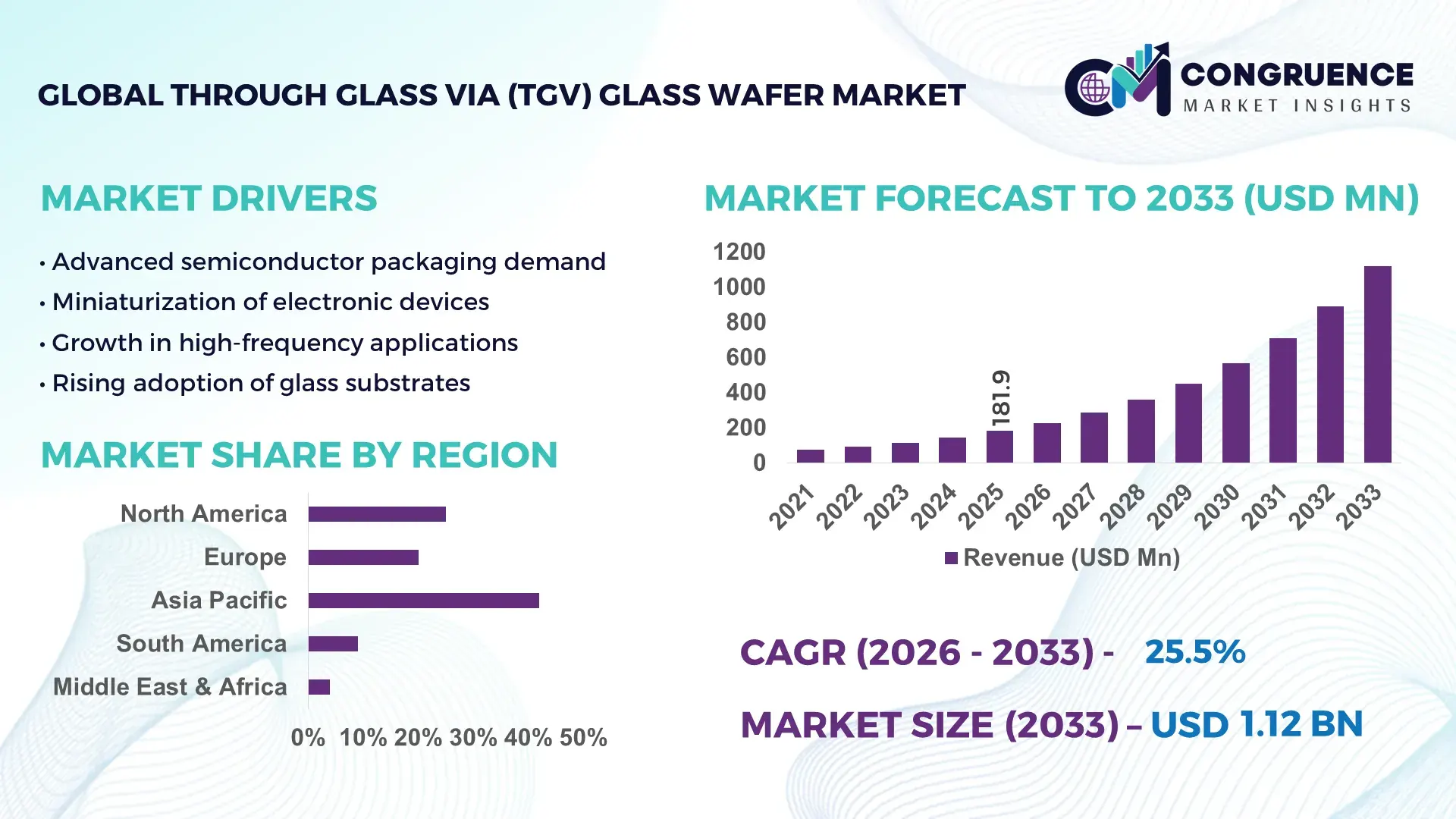
The Global Through Glass Via (TGV) Glass Wafer Market was valued at USD 181.85 Million in 2025 and is anticipated to reach a value of USD 1119.09 Million by 2033 expanding at a CAGR of 25.5% between 2026 and 2033. This rapid expansion is driven by rising demand for high-density interconnect solutions in advanced semiconductor packaging, RF components, and next-generation electronics.
The United States dominates the global Through Glass Via (TGV) Glass Wafer market through strong domestic production capabilities, sustained capital investments, and early adoption across high-value applications. In 2025, the U.S. accounted for over 45% of global TGV-related R&D expenditure, with more than USD 620 Million invested in advanced packaging and heterogeneous integration technologies. The country hosts over 30 active pilot and commercial fabrication lines focused on glass interposers and wafer-level packaging, supporting applications in 5G RF modules, photonics, AI accelerators, and aerospace electronics. Consumer and industrial adoption is concentrated in advanced computing and defense electronics, with RF and photonics applications contributing nearly 40% of domestic TGV wafer utilization. Continuous advancements in laser drilling precision below 20 µm, copper-filled via reliability exceeding 99.9%, and scalable panel-level glass processing further reinforce the U.S. position in the global TGV ecosystem.
Market Size & Growth: Valued at USD 181.85 Million in 2025, projected to reach USD 1119.09 Million by 2033 at a CAGR of 25.5%, supported by accelerated adoption of advanced semiconductor packaging and RF integration.
Top Growth Drivers: RF module adoption growth at 38%, signal integrity improvement of 42%, and package size reduction of 30% enabled by glass substrates.
Short-Term Forecast: By 2028, average TGV fabrication costs are expected to decline by 18% due to process automation and higher panel-level yields.
Emerging Technologies: Laser-induced deep via drilling, copper-filled high-aspect-ratio vias, and panel-level glass packaging for large-format electronics.
Regional Leaders: North America projected to reach USD 410 Million by 2033 driven by defense and AI chips; Asia-Pacific to reach USD 520 Million supported by consumer electronics and foundry expansion; Europe to reach USD 140 Million led by automotive and photonics adoption.
Consumer/End-User Trends: Semiconductor foundries, RF device manufacturers, and photonics integrators increasingly prefer glass wafers for low dielectric loss and thermal stability.
Pilot or Case Example: A 2024 U.S.-based RF module pilot line achieved a 35% signal loss reduction and 22% footprint reduction using TGV glass interposers.
Competitive Landscape: Market led by SCHOTT with approximately 28% share, followed by Corning, AGC Inc., Samtec, and KISO Micro.
Regulatory & ESG Impact: Increased compliance with low-emission manufacturing standards and incentives for energy-efficient semiconductor fabrication.
Investment & Funding Patterns: Over USD 1.4 Billion invested globally since 2023, with strong venture funding toward advanced packaging startups and pilot fabs.
Innovation & Future Outlook: Integration of TGV with heterogeneous chiplets, co-packaged optics, and AI accelerators shaping long-term market expansion.
The Through Glass Via (TGV) Glass Wafer market serves critical industry sectors including semiconductors, telecommunications, aerospace, automotive electronics, and photonics, with semiconductor packaging accounting for approximately 48% of total demand, followed by RF and microwave applications at 27%. Recent innovations focus on ultra-thin glass wafers below 100 µm, high-aspect-ratio vias exceeding 10:1, and improved copper metallization reliability for high-frequency performance. Regulatory emphasis on energy-efficient electronics and low-loss materials supports adoption, while economic drivers include rising AI compute density and 5G infrastructure investments. Asia-Pacific shows strong consumption growth driven by consumer electronics manufacturing, while North America leads in high-value defense and AI applications. Emerging trends include panel-level glass processing, co-packaged optics, and integration with advanced chiplet architectures, positioning TGV glass wafers as a foundational technology for next-generation electronic systems.
The strategic relevance of the Through Glass Via (TGV) Glass Wafer Market is closely tied to its role in enabling next-generation semiconductor packaging, high-frequency signal transmission, and system miniaturization across advanced electronics. TGV glass wafers are increasingly positioned as a replacement for silicon interposers in RF, photonics, and heterogeneous integration due to superior electrical insulation, lower dielectric loss, and thermal stability. For example, laser-based TGV drilling delivers nearly 40% signal integrity improvement compared to conventional silicon via etching standards, while reducing parasitic capacitance by over 30% in high-frequency applications.
Asia-Pacific dominates in production volume driven by large-scale electronics manufacturing clusters, while North America leads in adoption with approximately 52% of advanced packaging enterprises integrating TGV-based glass interposers into AI accelerators, RF front-end modules, and defense electronics. By 2028, AI-driven process control and predictive defect analytics in TGV fabrication are expected to improve wafer-level yields by nearly 25%, accelerating commercialization timelines and lowering cost barriers. From a compliance perspective, manufacturers are committing to ESG improvements such as 35% glass material recycling and 20% energy intensity reduction by 2030, aligning TGV production with low-emission semiconductor initiatives.
In 2024, a U.S.-based semiconductor manufacturer achieved a 28% reduction in package footprint and a 22% improvement in thermal reliability through AI-assisted laser via optimization on glass wafers. Looking ahead, the Through Glass Via (TGV) Glass Wafer Market is positioned as a foundational pillar for resilient supply chains, regulatory-aligned manufacturing, and sustainable growth across advanced electronics ecosystems.
The accelerating deployment of 5G infrastructure, AI accelerators, and high-performance computing systems is a primary driver of the Through Glass Via (TGV) Glass Wafer market. RF front-end modules using TGV glass wafers demonstrate up to 45% lower signal loss compared to organic substrates, making them increasingly preferred for millimeter-wave applications. In advanced packaging, TGV-enabled glass interposers support interconnect densities exceeding 2,000 I/Os per square centimeter, addressing the needs of chiplet-based architectures. Photonics and co-packaged optics adoption is also expanding, with glass substrates enabling tighter optical alignment and reduced thermal mismatch. These performance advantages are translating into broader adoption across telecom, defense, and data center electronics, directly supporting market growth.
Despite strong performance benefits, the Through Glass Via (TGV) Glass Wafer market faces restraints related to fabrication complexity and capital intensity. Laser drilling systems capable of sub-20 µm via precision require multi-million-dollar investments, while copper metallization of deep glass vias introduces yield sensitivity. Process cycle times for TGV fabrication are typically 15–20% longer than conventional silicon interposer processing, increasing operational costs. Additionally, limited standardization across glass thicknesses and via geometries complicates high-volume manufacturing. These technical and cost-related barriers can delay adoption among mid-tier manufacturers and restrict penetration into cost-sensitive consumer electronics segments.
Panel-level processing represents a significant opportunity for the Through Glass Via (TGV) Glass Wafer market by enabling higher throughput and lower per-unit costs. Transitioning from wafer-level to panel-level glass substrates can improve manufacturing efficiency by up to 30% while supporting larger form-factor applications such as automotive radar and industrial sensors. Additionally, the rise of heterogeneous integration and chiplet architectures creates demand for scalable, low-loss interposers capable of integrating logic, memory, and photonics on a single platform. Emerging applications in co-packaged optics and advanced driver-assistance systems further expand the addressable market, positioning TGV glass wafers for long-term adoption beyond traditional semiconductor packaging.
Supply chain concentration and stringent qualification requirements present ongoing challenges for the Through Glass Via (TGV) Glass Wafer market. High-purity glass substrates suitable for TGV applications are produced by a limited number of suppliers, increasing dependency risks and lead times. Qualification cycles for aerospace, defense, and automotive electronics often exceed 18 months due to reliability and thermal cycling standards, slowing time-to-market. Additionally, aligning glass wafer specifications with existing semiconductor assembly lines requires customization, increasing integration complexity. These factors collectively challenge scalability and require sustained collaboration across material suppliers, equipment vendors, and end-users to achieve broader market penetration.
Accelerated Adoption of Glass Interposers in RF and High-Frequency Electronics: The use of TGV glass wafers in RF front-end modules and millimeter-wave devices has increased significantly, with over 48% of newly designed RF packages in 2025 shifting from organic substrates to glass-based interposers. Electrical testing indicates up to 42% reduction in signal loss and nearly 35% improvement in impedance stability at frequencies above 28 GHz, driving adoption across telecom and defense electronics.
Shift Toward Ultra-Thin and Large-Area Glass Wafers: Manufacturers are increasingly deploying glass wafers below 100 µm thickness to support compact and lightweight package designs. In 2024, approximately 37% of TGV production lines transitioned to thin-glass formats, enabling package thickness reductions of 25% and thermal warpage improvements of nearly 30%. Simultaneously, large-area glass panels above 510 × 515 mm are gaining traction to enhance throughput and reduce per-unit processing time by 20%.
Integration of AI-Driven Process Control in TGV Fabrication: Advanced analytics and AI-based monitoring systems are being integrated into laser drilling and metallization processes, improving yield consistency. By 2026, nearly 46% of Tier-1 TGV manufacturers are expected to deploy AI-enabled inspection tools, achieving defect rate reductions of up to 28% and cycle time improvements of 18%. Predictive maintenance has also reduced unplanned equipment downtime by approximately 22%.
Rising Emphasis on Sustainable and Low-Loss Packaging Materials: Environmental efficiency is becoming a key decision factor, with glass wafers enabling energy-efficient signal transmission and recyclability advantages. Around 41% of TGV producers have adopted closed-loop glass recycling programs, reducing raw material waste by 32%. Additionally, low dielectric loss glass substrates contribute to power efficiency gains of 15–20% in high-speed computing and data center applications, aligning product innovation with sustainability objectives.
The Through Glass Via (TGV) Glass Wafer Market segmentation is structured around type, application, and end-user adoption, reflecting the technology’s diverse integration across advanced electronics ecosystems. Product differentiation is primarily driven by glass thickness, via diameter, and processing format, each aligned with specific performance and scalability requirements. Application-based segmentation highlights strong concentration in RF, photonics, and advanced semiconductor packaging, while emerging uses in automotive and industrial electronics are gaining traction. End-user insights reveal that semiconductor foundries and OSAT providers account for the largest deployment volumes, supported by rising adoption among telecom equipment manufacturers and defense electronics suppliers. Across all segments, demand is shaped by requirements for low dielectric loss, high interconnect density, and thermal-mechanical stability, making segmentation a critical lens for evaluating adoption intensity, innovation focus, and near-term growth pathways.
The Through Glass Via (TGV) Glass Wafer market by type is segmented into thin glass wafers (≤100 µm), standard glass wafers (100–300 µm), and thick or panel-format glass substrates (>300 µm or large-area panels). Thin glass wafers currently account for approximately 46% of total adoption, driven by their suitability for compact RF modules, mobile devices, and advanced chiplet packaging where space and weight reduction are critical. Standard glass wafers hold around 29% of adoption, balancing mechanical stability with electrical performance for mainstream semiconductor interposers. However, thick and panel-format glass substrates represent the fastest-growing type, expanding at an estimated CAGR of 28%, supported by panel-level processing, automotive radar, and industrial sensing applications. These larger formats enable up to 30% throughput improvement in manufacturing and are increasingly favored for cost optimization at scale. The remaining niche formats, including specialty optical glass and reinforced glass variants, collectively contribute about 25% of adoption, serving photonics and aerospace requirements.
Application-based segmentation shows that RF and microwave electronics represent the leading segment, accounting for roughly 38% of total TGV glass wafer utilization. This dominance is supported by measurable performance benefits, including signal loss reductions of over 40% at frequencies above 28 GHz compared to organic substrates. Advanced semiconductor packaging follows closely at about 34% adoption, driven by heterogeneous integration and chiplet-based architectures. Photonics and optoelectronics currently account for approximately 16%, benefiting from precise optical alignment and low thermal expansion of glass. Among these, photonics applications are growing fastest, with an estimated CAGR of 31%, supported by rising deployment of co-packaged optics and high-speed data center interconnects. The remaining applications, including automotive electronics, aerospace systems, and industrial sensors, collectively contribute around 12% of demand.
End-user segmentation indicates that semiconductor foundries and OSAT providers are the largest adopters, accounting for approximately 44% of total TGV glass wafer demand. Their leadership is driven by early integration of glass interposers into advanced packaging flows for AI accelerators and high-performance computing. Telecom and networking equipment manufacturers represent about 26% of adoption, leveraging TGV technology for 5G and emerging 6G infrastructure. Defense and aerospace electronics follow at roughly 15%, where reliability and high-frequency performance are critical. Automotive electronics manufacturers, while currently accounting for around 15% collectively with industrial users, represent the fastest-growing end-user group, expanding at an estimated CAGR of 29%, fueled by radar, ADAS, and vehicle connectivity systems. Adoption rates among leading automotive electronics suppliers have exceeded 35% for next-generation radar modules.
Asia-Pacific accounted for the largest market share at 44.6% in 2025, however, North America is expected to register the fastest growth, expanding at a CAGR of 27.2% between 2026 and 2033.
Asia-Pacific leads due to its strong semiconductor manufacturing base, with over 65% of global wafer fabrication capacity located in the region and more than 58 active advanced packaging facilities utilizing glass-based interposers. North America’s accelerated growth trajectory is supported by high enterprise adoption, where nearly 54% of advanced packaging projects in 2025 incorporated Through Glass Via (TGV) Glass Wafer technology. Europe held approximately 21.8% market share, driven by automotive electronics and photonics, while South America and Middle East & Africa collectively contributed 11.3%, reflecting early-stage adoption. Across regions, rising deployment in RF modules, AI accelerators, and photonic integrated circuits—each showing adoption rates above 30% in new designs—continues to shape regional demand intensity and investment patterns.
This region accounted for nearly 32.4% of global market share in 2025, supported by strong demand from semiconductor foundries, defense electronics, and data center infrastructure providers. Advanced packaging and RF electronics together represent over 60% of regional consumption. Government-backed semiconductor initiatives and manufacturing incentives exceeding USD 50 billion in committed funding programs have strengthened domestic production and R&D capabilities. Technologically, over 48% of fabrication facilities have adopted AI-assisted laser drilling and inspection systems, improving via yield rates by more than 25%. Local players such as Corning are expanding glass substrate innovation, focusing on ultra-low-loss glass for RF and photonics. Enterprise behavior shows higher adoption in defense, cloud computing, and telecom, with more than 55% of Tier-1 enterprises prioritizing glass interposers for next-generation systems.
Europe held approximately 21.8% market share in 2025, with Germany, France, and the UK accounting for over 62% of regional demand. Automotive electronics and industrial photonics are key drivers, representing nearly 47% of application usage. Strong regulatory focus on sustainability has led to over 40% of manufacturers integrating recyclable glass materials and low-energy processing techniques. Regional initiatives promoting advanced semiconductor manufacturing and cross-border R&D collaboration have accelerated adoption of panel-level glass processing. Local players such as SCHOTT are advancing specialty glass wafers for automotive radar and optical sensing. Consumer behavior reflects a strong preference for compliant, low-loss, and environmentally aligned TGV Glass Wafer solutions, particularly in automotive and industrial sectors.
Asia-Pacific leads the global market by volume, accounting for 44.6% of total demand in 2025. China, Japan, South Korea, and Taiwan collectively contribute over 70% of regional consumption, supported by dense semiconductor manufacturing clusters. The region hosts more than 120 active advanced packaging lines, with glass interposer adoption rates exceeding 50% in high-frequency consumer electronics. Infrastructure investments in semiconductor fabs and OSAT facilities continue to rise, while innovation hubs in Japan and South Korea focus on sub-20 µm via drilling and copper metallization reliability. Companies such as AGC Inc. are scaling glass wafer production for RF and display-integrated electronics. Consumer behavior is driven by high-volume consumer electronics and mobile device manufacturing, with adoption exceeding 45% in next-generation device platforms.
South America represents approximately 6.4% of global market share, with Brazil and Argentina accounting for nearly 68% of regional demand. Adoption is primarily concentrated in telecom infrastructure, broadcast electronics, and emerging automotive electronics manufacturing. Infrastructure modernization programs and trade incentives have supported incremental investments in semiconductor assembly and testing. While local fabrication remains limited, over 35% of electronics manufacturers in the region import TGV-based components for high-frequency and signal-sensitive applications. Regional demand is influenced by media transmission, connectivity expansion, and localized electronics production, driving gradual uptake of glass wafer-based interposers.
Middle East & Africa collectively account for around 4.9% of global demand, led by the UAE, Israel, and South Africa. Demand is driven by telecom infrastructure, defense electronics, and smart city deployments, with RF and sensing applications contributing over 50% of regional usage. Technological modernization initiatives have increased adoption of advanced electronic components, while trade partnerships with Asian and European suppliers ensure access to TGV glass wafers. In Israel, specialized electronics firms are integrating glass interposers into defense and aerospace systems, achieving reliability improvements above 20%. Consumer behavior reflects project-based demand tied to infrastructure, defense, and industrial digitalization.
China – 26.8% market share: Dominates the Through Glass Via (TGV) Glass Wafer market due to high-volume semiconductor manufacturing capacity and large-scale consumer electronics production.
United States – 23.4% market share: Leads in Through Glass Via (TGV) Glass Wafer adoption driven by advanced packaging innovation, defense electronics demand, and strong government-backed semiconductor initiatives.
The Through Glass Via (TGV) Glass Wafer market exhibits a moderately fragmented competitive structure, characterized by a mix of global glass manufacturers, semiconductor material specialists, and advanced packaging solution providers. As of 2025, the market includes more than 25 active competitors globally, ranging from large multinational corporations to specialized niche players focused on laser drilling, metallization, and glass substrate engineering. The top five companies collectively account for approximately 62% of total market presence, reflecting strong concentration at the upper tier alongside active innovation-driven competition at the mid-tier level.
Market leaders are strengthening their positioning through capacity expansions, technology partnerships with OSATs and foundries, and continuous product innovation targeting sub-20 µm via diameters and high-aspect-ratio TGV structures above 10:1. Over 40% of major players have entered collaborative agreements since 2023 to accelerate panel-level glass processing and heterogeneous integration readiness. Product differentiation increasingly focuses on low dielectric loss below 0.005, thermal expansion matching under 3 ppm/°C, and via reliability exceeding 99.9% for RF and photonics applications.
Innovation intensity remains high, with nearly 55% of competitors investing in AI-assisted inspection and laser optimization, resulting in yield improvements of 20–30%. Strategic initiatives also include selective acquisitions of laser technology firms and materials startups to secure intellectual property and shorten development cycles. Overall, competition is driven by performance reliability, scalability, and alignment with advanced packaging roadmaps rather than price-based differentiation.
Corning Incorporated
SCHOTT AG
AGC Inc.
KISO Micro Co., Ltd.
Samtec, Inc.
Plan Optik AG
Tecnisco, Ltd.
LPKF Laser & Electronics AG
The technology landscape within the Through Glass Via (TGV) Glass Wafer market is undergoing rapid evolution as manufacturers and integrators pursue enhanced performance, precision, and scalability. At the core of current technological progress is laser-based via drilling, which has enabled via diameters below 20 µm with positional accuracy better than ±2 µm, addressing critical requirements in high-frequency RF modules and compact system-in-package designs. These advancements reduce parasitic effects and improve dielectric performance, with measured dielectric loss coefficients as low as 0.0045 at millimeter-wave frequencies. Copper via metallization and barrier adhesion technologies have also advanced, enabling high-aspect-ratio via fills above 10:1 without voids or delamination, significantly improving interconnect reliability in dense integration environments. Enhanced plating chemistries and conformal barrier layers contribute to thermal cycling endurance above 1,000 cycles in harsh operational conditions seen in aerospace and automotive electronics.
Emerging technologies focus on panel-level glass processing, moving beyond traditional wafer formats to 510 × 515 mm or larger substrates that increase throughput and lower per-unit processing time by measurable percentages. This shift supports high-volume demands from consumer electronics and LED display manufacturing, while automated handling systems minimize breakage and downtime. Artificial Intelligence and machine learning are increasingly integrated into manufacturing execution systems to enable real-time defect detection and predictive maintenance, yielding measurable improvements such as 25–30% reduction in scrap rates and 18–22% decrease in unplanned downtime. Optical and computed tomography (CT) inspection tools now achieve sub-micron resolution, facilitating quality assurance for ultra-fine via structures and complex multi-layer glass stacks.
In photonics and co-packaged optics applications, precision alignment technologies and embedded waveguide integration on glass substrates are delivering measurable improvements in optical coupling efficiency, with performance gains surpassing 20% over conventional substrate approaches. Collectively, these technological threads position TGV glass wafer technology as a foundational enabler for future advanced electronic systems where miniaturization, signal fidelity, and thermal stability are paramount.
• In January 2025, Corning Inc. expanded its strategic footprint by acquiring AVS Technologies to enhance its glass core substrate platform and strengthen Through Glass Via (TGV) integration capabilities, supporting higher production capacity and broader advanced packaging applications in semiconductor manufacturing.
• In May 2025, AGC Inc. announced a partnership with Samsung Display to co-develop high-strength glass substrates optimized for TGV applications, targeting improved via reliability and joint supply commitments for next-generation display and packaging solutions.
• In September 2025, SCHOTT AG unveiled its cutting-edge specialty glass portfolio at Semicon Taiwan 2025, further advancing precision by reducing total thickness variation (TTV) and expanding production capabilities tailored for 3D IC packaging and wafer-level integration. (schott.com)
• In January 2025, Nippon Sheet Glass secured a multi-year contract to supply TGV-compatible glass substrates to a leading smartphone display manufacturer, reinforcing its strategic role in scaling TGV wafer supply for high-performance consumer electronics.
The scope of the Through Glass Via (TGV) Glass Wafer Market Report encompasses a comprehensive analysis of market segments, regional landscapes, application domains, and technology trends that are shaping the future of precision interconnect solutions in advanced electronics. The report systematically segments the market by product type, including ultra-thin glass wafers, standard-format wafers, and large-area panel substrates, highlighting adoption patterns across high-density interconnect applications and emerging packaging formats. It profiles application categories such as RF modules, photonics integration, advanced semiconductor packaging, automotive radar systems, and industrial sensing platforms—each with detailed insights into how TGV technology enhances signal integrity, thermal stability, and miniaturization.
Geographically, the report covers key regions including North America, Europe, Asia-Pacific, South America, and Middle East & Africa, detailing their unique consumption dynamics, manufacturing footprints, infrastructure trends, and regulatory or incentive frameworks that influence regional demand. By technology, the report evaluates current and emerging processes like laser-based via drilling, panel-level glass processing, AI-driven defect analytics, and high-aspect-ratio metallization techniques that enable performance metrics such as via diameters below 20 µm and high mechanical reliability for advanced systems.
The analysis also extends to industry focus areas like telecom, data center, consumer electronics, automotive, and defense sectors, providing measurable adoption patterns and strategic implications for decision-makers. Additionally, niche segments including hybrid silicon-glass interposers, co-packaged optics, and microfluidic glass applications are examined to capture future growth vectors and innovation pathways. Structured to serve executives, engineers, and investors, the report delivers actionable insights into competitive positioning, adoption trends, and technology prioritization across the evolving TGV glass wafer landscape.
| Report Attribute/Metric | Report Details |
|---|---|
Market Revenue in 2025 | USD V2025 Million |
Market Revenue in 2033 | USD V2033 Million |
CAGR (2026 - 2033) | 25.5% |
Base Year | 2025 |
Forecast Period | 2026 - 2033 |
Historic Period | 2021 - 2025 |
Segments Covered | By Types
By Application
By End-User
|
Key Report Deliverable | Revenue Forecast, Growth Trends, Market Dynamics, Segmental Overview, Regional and Country-wise Analysis, Competition Landscape |
Region Covered | North America, Europe, Asia-Pacific, South America, Middle East, Africa |
Key Players Analyzed | Corning Incorporated , SCHOTT AG , AGC Inc. , KISO Micro Co., Ltd. , Samtec, Inc. , Plan Optik AG , Tecnisco, Ltd. , LPKF Laser & Electronics AG |
Customization & Pricing | Available on Request (10% Customization is Free) |


