
Reports
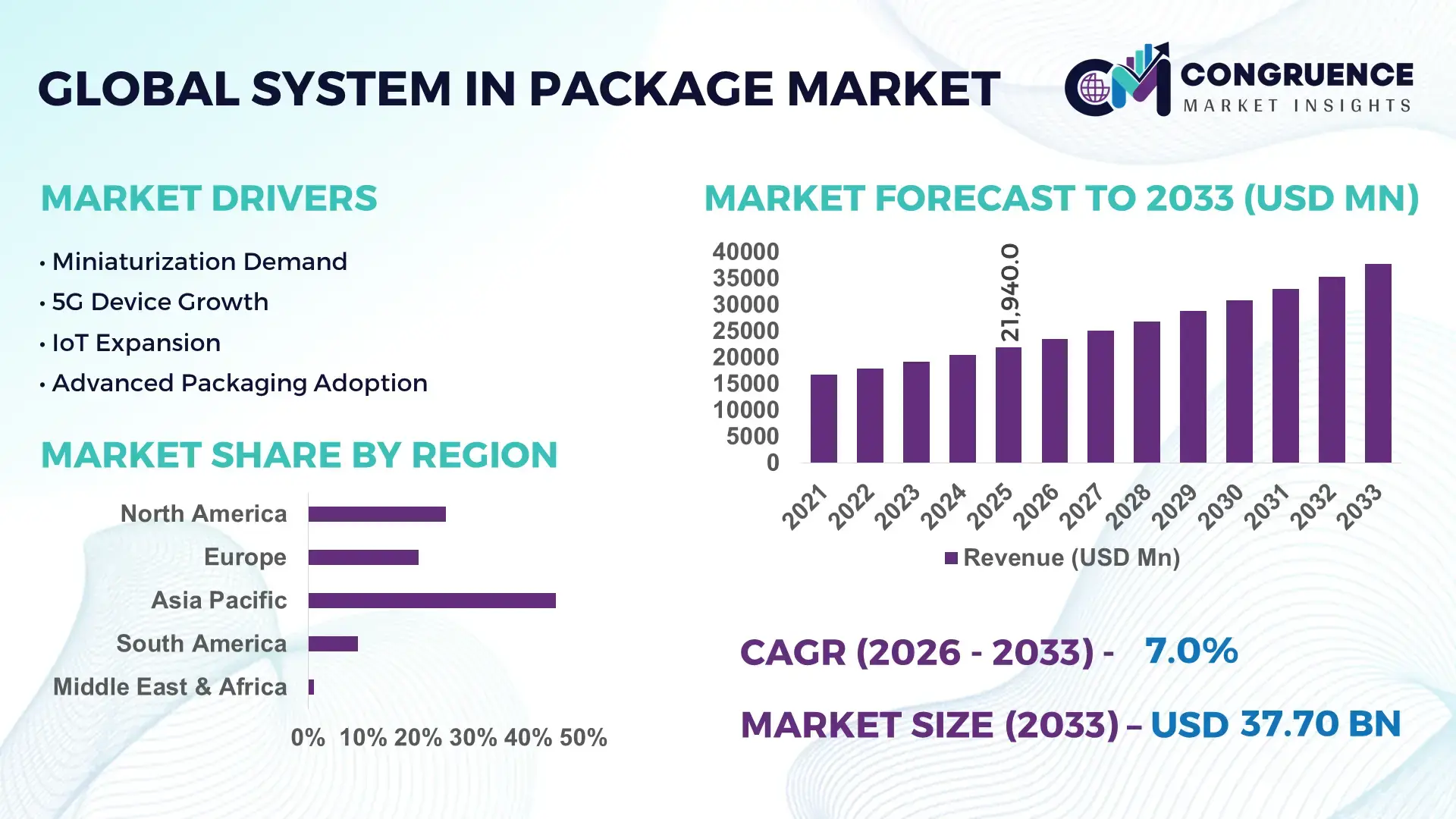
The Global System in Package Market was valued at USD 21940 Million in 2025 and is anticipated to reach a value of USD 37697 Million by 2033 expanding at a CAGR of 7% between 2026 and 2033.
The market is being structurally driven by the shift toward heterogeneous integration, where combining multiple chips in a single package reduces footprint by over 35% and improves performance efficiency by nearly 25% compared to traditional PCB-based designs. Between 2024 and 2026, global semiconductor supply chains have undergone regional diversification due to geopolitical trade realignments and export controls, accelerating localized packaging investments across Asia and North America. This shift has increased backend semiconductor capacity expansion by approximately 18%, directly benefiting advanced packaging technologies such as System in Package.
China remains the dominant country, accounting for nearly 32% of global packaging capacity, supported by over USD 12 billion in recent semiconductor packaging investments and strong demand from consumer electronics and automotive electronics sectors. The country’s OSAT (outsourced semiconductor assembly and test) industry has expanded production efficiency by 20% through automation and AI integration, while Taiwan follows with around 25% share, driven by advanced node packaging for high-performance computing applications. Compared to conventional packaging, SiP adoption in these regions delivers up to 30% higher integration density, enabling competitive differentiation for OEMs.
Strategically, companies prioritizing advanced packaging ecosystems and regional supply resilience will capture higher margins and secure long-term technology leadership.
Market Size & Growth: USD 21,940M (2025) to USD 37,697M (2033) at 7% CAGR, driven by advanced semiconductor miniaturization and high-density integration demand.
Top Growth Drivers: Integration efficiency (+35%), device miniaturization (+28%), and 5G/IoT adoption (+40%).
Short-Term Forecast: By 2027, packaging costs decline by 18% while performance efficiency improves by 22% through automation.
Emerging Technologies: AI-enabled packaging, fan-out wafer-level packaging, and 3D stacking improving performance by 25–30%.
Regional Leaders: Asia-Pacific (~USD 18B) leads with 60% adoption, North America (~USD 9B) focuses on advanced packaging R&D, Europe (~USD 6B) driven by automotive electronics growth.
Consumer/End-User Trends: Over 55% of consumer electronics manufacturers adopt SiP for compact device design and energy efficiency gains.
Pilot/Case Example: In 2025, a leading semiconductor firm achieved 27% power reduction using 3D SiP integration in mobile processors.
Competitive Landscape: Top player holds ~14% share, with key firms including major OSAT and integrated device manufacturers driving innovation.
Regulatory & ESG Impact: Energy-efficient packaging reduces power consumption by 20%, aligning with global semiconductor sustainability mandates.
Investment & Funding: Over USD 15B invested globally in advanced packaging expansion amid supply chain diversification trends.
Innovation & Future Outlook: Next-gen heterogeneous integration and chiplet-based architectures drive 30% higher performance scaling.
The consumer electronics segment contributes approximately 42% of total demand, followed by automotive electronics at 26% and telecommunications at 18%, reflecting strong diversification across high-growth industries. Recent innovations such as chiplet-based SiP architectures and fan-out packaging have improved thermal efficiency by nearly 20%, addressing performance bottlenecks in compact devices. Asia-Pacific dominates with over 60% demand share, supported by manufacturing scale, while North America is advancing design innovation amid supply chain localization efforts. An emerging trend toward AI-integrated packaging is accelerating performance optimization, positioning the market for deeper vertical integration and strategic technology partnerships.
System in Package is rapidly becoming a decisive battleground for semiconductor competitiveness, as device manufacturers prioritize integration density, power efficiency, and form-factor optimization to differentiate in saturated electronics markets. The technology is transforming how performance scaling is achieved, shifting value creation from pure node advancement to packaging-led innovation, where integration efficiency gains of over 30% directly translate into faster product cycles and higher margin potential.
A major structural shift is underway as supply chains move from centralized semiconductor ecosystems toward regionally diversified packaging hubs, driven by geopolitical trade controls and national semiconductor policies. In this context, fan-out wafer-level packaging improves efficiency by 28% while reducing cost by 18% compared to legacy wire-bond packaging systems, making it a commercially superior choice for high-volume applications. Asia-Pacific leads in volume with over 60% of global production capacity, while North America leads in innovation intensity with over 35% of advanced packaging R&D investments focused on chiplet integration and heterogeneous architectures. Over the next 2–3 years, production cycle times are expected to decline by 20%, while yield efficiency improves by approximately 15%, enabling faster commercialization of complex semiconductor designs.
Sustainability is emerging as a competitive advantage, with energy-efficient SiP designs reducing power consumption by up to 22%, allowing companies to meet tightening ESG compliance standards while lowering operational costs. A notable 2025 deployment in automotive control units demonstrated a 25% reduction in thermal losses through advanced SiP integration, directly improving reliability and lifecycle performance. Leading semiconductor firms are accelerating capital allocation toward advanced packaging, with over 40% of new backend investments directed to SiP and chiplet ecosystems, signaling a strategic pivot away from traditional scaling models. Companies that optimize packaging innovation alongside supply chain resilience are positioning themselves to dominate next-generation electronics markets and secure long-term technological leadership.
The accelerating demand for compact, high-performance electronics is forcing a structural transition toward heterogeneous integration, where multiple functional chips are combined into a single package to deliver up to 35% higher performance efficiency and 30% space reduction. This shift is strongly driven by the expansion of 5G infrastructure and AI-enabled devices, where processing density and thermal management are critical. A key global trigger is the ongoing semiconductor supply chain restructuring, which has increased regional backend capacity investments by nearly 18%, reinforcing the role of advanced packaging as a strategic priority. As a result, companies are rapidly expanding OSAT capabilities, forming strategic partnerships with foundries, and increasing capital allocation toward automation-driven packaging lines. This cause-and-effect dynamic is accelerating production scalability while enabling faster time-to-market, directly strengthening competitive positioning in high-growth sectors such as automotive electronics and consumer devices.
Despite strong demand momentum, the System in Package market faces structural constraints linked to material dependency and cost volatility, particularly in advanced substrates and high-density interconnect materials, where price fluctuations have reached 12–15% annually. Additionally, over 70% of critical packaging substrates are concentrated in a limited number of suppliers across Asia, creating supply bottlenecks and increasing lead times by up to 20%. These constraints directly impact production scalability and cost predictability, especially for companies operating in high-volume consumer electronics markets. Regulatory pressures around semiconductor localization further complicate sourcing strategies, forcing firms to invest in redundant supply chains. To mitigate these risks, companies are diversifying supplier networks, entering long-term procurement agreements, and investing in alternative materials and packaging techniques. These actions are critical to stabilizing cost structures and maintaining consistent production output under volatile market conditions.
The transition toward chiplet-based architectures and AI-driven semiconductor applications is unlocking high-value opportunities within the System in Package market, with chiplet integration improving processing efficiency by nearly 25% while reducing development cycles by 20%. Emerging markets in electric vehicles and industrial automation are driving demand for highly integrated, energy-efficient modules, creating new revenue streams for advanced packaging providers. A key innovation shift is the adoption of 3D stacking and fan-out technologies, which enhance thermal performance by over 18%, enabling next-generation computing and edge AI applications. Companies are strategically positioning themselves by expanding R&D capabilities, building ecosystem partnerships across design and manufacturing, and investing in localized production facilities to capture regional demand growth. This forward-looking approach is not only optimizing operational efficiency but also establishing long-term dominance in emerging semiconductor value chains.
The primary challenge in scaling System in Package technologies lies in managing complexity across design, manufacturing, and testing processes, where integration errors can reduce yield rates by up to 15%. Infrastructure limitations, particularly in advanced testing and inspection capabilities, create bottlenecks that extend production timelines by nearly 18%. Additionally, increasing design complexity driven by multi-chip integration is placing pressure on thermal management and reliability standards, especially in automotive and high-performance computing applications. A real-world pressure point is the growing mismatch between rapid design innovation and slower backend manufacturing upgrades, constraining overall ecosystem efficiency. To remain competitive, companies must invest heavily in advanced testing infrastructure, adopt AI-driven quality control systems, and strengthen cross-industry collaborations to align design and manufacturing capabilities. Addressing these execution barriers is essential for sustaining long-term growth and ensuring consistent performance delivery in increasingly complex semiconductor environments.
Over 38% shift toward fan-out packaging is reshaping assembly workflows. Manufacturers are rapidly transitioning from traditional substrate-based packaging to fan-out wafer-level processes, increasing throughput by nearly 22% while reducing package thickness by 30%. This shift is being executed through automation upgrades and reconfigured backend lines, enabling faster cycle times and improved yield consistency. Companies are scaling fan-out capacity and forming equipment partnerships to handle higher wafer volumes, directly lowering unit costs and improving margin stability.
Advanced automation adoption exceeding 45% is optimizing backend efficiency. Packaging facilities are integrating AI-driven inspection and robotics, reducing defect rates by up to 18% and improving operational efficiency by 20%. Labor constraints and rising wage pressures in Asia have acted as real-world triggers, forcing companies to accelerate automation deployment. This operational shift is redefining cost structures, with firms restructuring production lines and investing in smart factories to maintain competitive throughput and quality benchmarks.
Regional demand realignment shows 25% capacity expansion outside traditional hubs. Companies are actively diversifying packaging operations beyond concentrated Asian clusters, with North America and Southeast Asia increasing backend capacity by 25% to mitigate geopolitical risks. This shift is happening through new facility setups and joint ventures, reducing supply chain dependency by approximately 15%. The non-obvious impact is improved supply resilience, allowing faster response to demand fluctuations while stabilizing delivery timelines for high-value semiconductor clients.
Outsourced packaging demand rising by 32% is redefining business models. Semiconductor firms are increasing reliance on OSAT providers to manage complexity and reduce capital intensity, cutting internal infrastructure costs by nearly 20%. This transition is being executed through long-term outsourcing contracts and strategic alliances, enabling faster scalability. Companies are repositioning toward asset-light models while OSAT players are expanding service portfolios, capturing higher-value integration work and strengthening their role in the semiconductor ecosystem.
The System in Package market is structured across technology types, applications, and end-user industries, with demand concentrated in high-performance, space-constrained electronic systems. Consumer-driven segments account for over 55% of total demand, while advanced industrial and automotive applications are rapidly increasing their share due to rising integration complexity. Demand is shifting toward high-density packaging formats as companies prioritize performance optimization and miniaturization. This segmentation highlights a clear transition from traditional packaging toward advanced, multi-functional integration, forcing companies to realign product strategies and invest in scalable, high-efficiency packaging technologies.
2D SiP continues to dominate with approximately 34% share, driven by its cost efficiency and established manufacturing ecosystem, making it the preferred choice for high-volume consumer electronics. However, 3D SiP is emerging as the fastest-growing segment, expanding at over 28% adoption growth due to its superior vertical stacking capability, delivering up to 30% higher performance density and improved power efficiency. The direct comparison highlights a clear shift: while 2D SiP offers scalability and lower cost, 3D SiP is redefining performance benchmarks for advanced computing and automotive applications.
2.5D SiP and Fan-Out SiP together account for nearly 40% share, with fan-out gaining traction due to its ability to reduce package size by over 25% while enhancing thermal performance. Flip-Chip SiP holds a niche yet strategic position with around 12% share, particularly in high-frequency telecom applications. Companies are actively reallocating investments toward 3D and fan-out technologies, expanding production capabilities and accelerating R&D to capture next-generation demand. The business implication is clear: investment focus is shifting toward high-density, performance-driven packaging, while legacy formats face gradual commoditization.
Consumer Electronics leads with nearly 38% share, driven by continuous demand for compact, multifunctional devices where integration efficiency directly impacts product competitiveness. Automotive Electronics is the fastest-growing segment, with adoption increasing by over 26% due to rising demand for advanced driver assistance systems and electric vehicle control units requiring high-reliability packaging solutions. The comparison between these segments shows a transition from volume-driven consumer demand to performance-critical automotive applications.
Mobile Devices and Telecom Equipment together contribute approximately 42% share, supported by 5G deployment and increasing data processing requirements. IoT Devices, though smaller at around 12%, are expanding steadily as edge computing adoption rises. Companies are responding by customizing packaging solutions for specific application needs, scaling production for consumer markets while investing in high-reliability designs for automotive and telecom sectors. This shift signals a move toward application-specific packaging strategies, where differentiation is driven by performance optimization rather than cost alone.
The Electronics Industry dominates with approximately 45% share, reflecting its high dependency on compact and high-performance semiconductor solutions for consumer and computing devices. The Automotive Sector is the fastest-growing end-user, with demand increasing by over 24% as electrification and autonomous systems require advanced packaging for reliability and thermal management. This contrast highlights a shift from volume-centric electronics manufacturing to performance-critical automotive integration.
Telecom and Industrial sectors together account for nearly 35% share, driven by infrastructure expansion and automation trends, while the Healthcare Industry represents around 10% with growing adoption in diagnostic and wearable devices. Companies are increasingly tailoring solutions through customization and strategic partnerships, offering specialized packaging for automotive and healthcare applications while maintaining scale efficiencies for electronics manufacturing. The business implication is clear: future demand is shifting toward high-reliability, application-specific solutions, requiring targeted investment and ecosystem collaboration to capture emerging opportunities.
Asia-Pacific accounted for the largest market share at 62% in 2025 however, North America is expected to register the fastest growth, expanding at a CAGR of 8.5% between 2026 and 2033.
Asia-Pacific leads in production scale and demand concentration, supported by over 70% of global semiconductor packaging capacity and strong electronics manufacturing ecosystems. North America, with nearly 18% share, is accelerating in advanced packaging innovation, driven by chiplet integration and localized semiconductor policies. Europe holds around 12% share, focusing on automotive and industrial applications with high-reliability packaging demand. A key structural shift is the global push for supply chain diversification, increasing backend capacity outside Asia by approximately 25%. Strategically, companies are balancing scale-driven operations in Asia with innovation and resilience investments in North America and Europe.
How is advanced packaging innovation accelerating high-performance semiconductor deployment?
North America holds approximately 18% of the global System in Package market, with demand concentrated in high-performance computing, telecom infrastructure, and defense electronics. The region is being reshaped by semiconductor localization policies, driving over 30% increase in domestic packaging investments. Companies are rapidly adopting chiplet-based SiP and 3D integration, improving performance efficiency by nearly 25%. A notable execution shift includes expansion of advanced packaging facilities, with capacity scaling initiatives increasing output by 20% in key technology hubs. Enterprises prioritize high-reliability and innovation-driven solutions over cost, accelerating adoption of advanced packaging technologies. This positions North America as a strategic center for next-generation semiconductor innovation, attracting sustained investment and technology leadership focus.
What role is compliance-driven innovation playing in advanced semiconductor packaging evolution?
Europe accounts for nearly 12% of the System in Package market, with key demand from Germany, France, and the Netherlands, particularly in automotive and industrial electronics. Strict ESG and energy-efficiency regulations are driving adoption of low-power SiP solutions, reducing energy consumption by up to 20%. Companies are shifting toward environmentally compliant manufacturing processes, increasing investment in sustainable packaging technologies by approximately 18%. Operationally, there is a strong focus on reliability and long lifecycle performance, especially in automotive applications. Enterprises demonstrate compliance-driven purchasing behavior, prioritizing quality and regulatory alignment over cost advantages. This regulatory environment is forcing continuous innovation, making Europe a critical region for advanced, sustainable semiconductor packaging development.
How is large-scale manufacturing transforming semiconductor packaging deployment speed?
Asia-Pacific dominates with over 62% market share, led by China, Taiwan, South Korea, and Japan, benefiting from extensive semiconductor manufacturing infrastructure and cost-efficient production ecosystems. The region handles more than 70% of global packaging output, with rapid adoption of fan-out and 3D SiP technologies improving efficiency by 25%. Execution-level shifts include large-scale automation and localized supply chain integration, increasing production speed by nearly 20%. Companies are aggressively expanding capacity, with several players increasing backend facilities by over 30% to meet global demand. Enterprises prioritize cost efficiency and speed-to-market, reinforcing Asia-Pacific’s dominance as the global hub for semiconductor packaging scale and supply reliability.
How are emerging electronics demands shaping localized semiconductor packaging adoption?
South America represents approximately 4% of the global System in Package market, with Brazil and Argentina leading demand, primarily driven by consumer electronics and telecom infrastructure expansion. The region faces structural limitations such as limited semiconductor manufacturing infrastructure and higher import dependency, increasing costs by nearly 15%. However, adoption is rising steadily, with localized assembly and packaging activities growing by around 12% as companies seek to reduce supply chain delays. Enterprises exhibit strong price sensitivity, favoring cost-effective packaging solutions over advanced integration. Strategic moves include partnerships with global suppliers to enhance local capabilities. This positions South America as a developing market with moderate growth potential but constrained scalability.
What infrastructure investments are enabling semiconductor packaging adoption across developing economies?
The Middle East & Africa region contributes close to 4% of the System in Package market, with demand driven by telecom expansion, smart infrastructure, and industrial automation projects in countries such as UAE and Saudi Arabia. Investment-led transformation is accelerating adoption, with infrastructure spending increasing by over 20% in key markets. Execution-level changes include deployment of advanced telecom systems and localized electronics assembly, boosting demand for efficient packaging solutions. A notable strategic move is the establishment of technology partnerships to support regional semiconductor capabilities. Enterprises prioritize long-term infrastructure performance and reliability, making this region an emerging strategic market with growing relevance for expansion-focused companies.
China – 32% share in the System in Package market, driven by large-scale semiconductor packaging capacity and strong consumer electronics manufacturing demand.
Taiwan – 25% share in the System in Package market, supported by advanced packaging innovation and leadership in high-performance computing applications.
The System in Package market is defined by intense competition between global OSAT leaders, integrated device manufacturers, and advanced packaging innovators, including players such as ASE Technology, Amkor Technology, JCET Group, TSMC, and Samsung Electronics. The top five players collectively control approximately 55% of the market, competing across technology leadership, cost efficiency, and supply chain control. Competition is increasingly technology-driven, with advanced packaging solutions delivering up to 30% higher performance efficiency and reducing system size by 25%, creating a clear differentiation advantage.
Global leaders are competing with regional players through capacity expansion and vertical integration, while technology innovators focus on chiplet architectures and 3D integration. Companies are actively forming strategic partnerships and expanding backend facilities, with capacity investments increasing by over 20% to secure long-term supply contracts. The competitive landscape is shifting toward advanced packaging ecosystems, where control over integration technology and supply chains determines market leadership. High capital requirements and technical complexity act as strong entry barriers, reinforcing the dominance of established players. Winning in this market requires continuous innovation, scale efficiency, and strategic ecosystem alignment.
ASE Technology Holding Co., Ltd.
Amkor Technology, Inc.
JCET Group Co., Ltd.
Taiwan Semiconductor Manufacturing Company (TSMC)
Samsung Electronics Co., Ltd.
Intel Corporation
Powertech Technology Inc.
Tongfu Microelectronics Co., Ltd.
ChipMOS Technologies Inc.
STATS ChipPAC Pte. Ltd.
UTAC Holdings Ltd.
Nepes Corporation
Signetics Corporation
System in Package technology is being reshaped by advanced integration techniques that directly impact performance and manufacturing efficiency. Current technologies such as flip-chip and fan-out wafer-level packaging are improving electrical performance by nearly 22% while reducing package size by up to 30%. Adoption levels have crossed 50% in high-volume consumer electronics, enabling faster assembly cycles and lowering per-unit production costs. This operational efficiency is allowing manufacturers to optimize throughput while maintaining competitive pricing in mass-market applications.
Emerging technologies including 2.5D and 3D SiP architectures are accelerating performance scaling, delivering up to 28% higher processing efficiency and 20% improved thermal management compared to conventional 2D designs. Deployment of these advanced formats has reached approximately 35% in high-performance computing and automotive sectors, where reliability and integration density are critical. Businesses are leveraging these technologies to enhance product differentiation, particularly in AI-enabled devices and electric vehicle systems, where compact design and performance optimization are essential.
Disruptive innovations such as chiplet-based architectures are redefining system design by enabling modular integration, reducing development cycles by nearly 25% while lowering design costs by 18% compared to monolithic systems. Compared to legacy packaging, these modular approaches improve scalability by over 30%, giving early adopters a clear competitive advantage. Leading semiconductor firms are investing heavily in ecosystem partnerships and advanced packaging R&D, positioning themselves to capture high-value segments between 2026 and 2028 as demand for heterogeneous integration continues accelerating.
March 2026 – Intel Corporation: Expanded advanced packaging capacity with a new facility scaling output by 20%, focusing on 3D chiplet integration to enhance high-performance computing efficiency. This strengthens domestic supply resilience and reduces dependency on offshore packaging providers. [Capacity Expansion] Source: https://www.intel.com
November 2025 – ASE Technology Holding: Introduced next-generation fan-out packaging improving thermal efficiency by 18% and reducing form factor by 25%, targeting mobile and AI applications. This innovation enhances product competitiveness and supports high-density integration demand. [Tech Innovation] Source: https://www.aseglobal.com
July 2025 – Amkor Technology: Announced strategic partnership with automotive OEMs to deploy SiP solutions, improving system reliability by 22% in EV control units. This move strengthens its position in the high-growth automotive electronics segment. [Strategic Partnership] Source: https://www.amkor.com
January 2024 – TSMC: Accelerated CoWoS advanced packaging deployment, increasing capacity by 15% to support AI chip demand. This directly improves processing throughput and positions the company as a leader in high-performance packaging ecosystems. [AI Scaling Push] Source: https://www.tsmc.com
The System in Package market report delivers comprehensive coverage across key segments, including types such as 2D, 2.5D, 3D, flip-chip, and fan-out SiP, alongside applications spanning consumer electronics, mobile devices, automotive electronics, telecom equipment, and IoT devices. It further evaluates end-user industries including electronics, automotive, telecom, industrial, and healthcare, while covering major geographic regions such as Asia-Pacific, North America, Europe, South America, and the Middle East & Africa. The report integrates analysis of advanced technologies including chiplet architectures, 3D stacking, and fan-out packaging, with adoption levels exceeding 40% in high-performance applications.
Analytical depth is reinforced through evaluation of over 15 key companies, 5 major regional markets, and multiple technology layers, supported by adoption insights such as over 60% demand concentration in Asia-Pacific and more than 35% deployment of advanced packaging in computing-intensive sectors. The report also captures emerging niches such as AI-integrated packaging and automotive-grade SiP, where efficiency gains exceed 20%.
Strategically, the report provides actionable intelligence for investment prioritization, capacity expansion, and competitive positioning, offering forward-looking coverage from 2026 to 2033. It enables decision-makers to identify high-impact growth areas, optimize technology adoption strategies, and align operations with evolving supply chain and integration trends.
| Report Attribute/Metric | Report Details |
|---|---|
|
Market Revenue in 2025 |
USD 21940 Million |
|
Market Revenue in 2033 |
USD 37697 Million |
|
CAGR (2026 - 2033) |
7% |
|
Base Year |
2025 |
|
Forecast Period |
2026 - 2033 |
|
Historic Period |
2021 - 2025 |
|
Segments Covered |
By Type
By Application
By End-User
|
|
Key Report Deliverable |
Revenue Forecast, Growth Trends, Market Dynamics, Segmental Overview, Regional and Country-wise Analysis, Competition Landscape |
|
Region Covered |
North America, Europe, Asia-Pacific, South America, Middle East, Africa |
|
Key Players Analyzed |
ASE Technology Holding Co., Ltd., Amkor Technology, Inc., JCET Group Co., Ltd., Taiwan Semiconductor Manufacturing Company (TSMC), Samsung Electronics Co., Ltd., Intel Corporation, Powertech Technology Inc., Tongfu Microelectronics Co., Ltd., ChipMOS Technologies Inc., STATS ChipPAC Pte. Ltd., UTAC Holdings Ltd., Nepes Corporation, Signetics Corporation |
|
Customization & Pricing |
Available on Request (10% Customization is Free) |


