
Reports
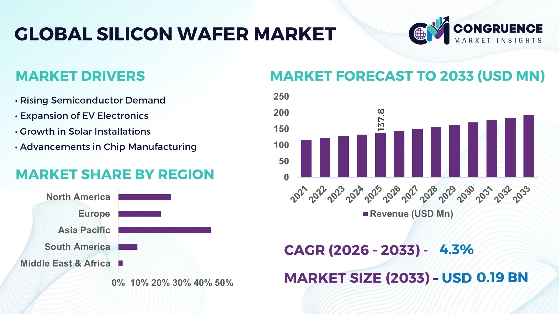
The Global Silicon Wafer Market was valued at USD 137.8 Million in 2025 and is anticipated to reach a value of USD 193.08 Million by 2033 expanding at a CAGR of 4.3% between 2026 and 2033. Rising deployment of AI accelerators, automotive power semiconductors, and advanced 300mm wafer fabrication lines is increasing high-purity silicon wafer consumption, with leading fabs improving wafer utilization efficiency by over 18% through process automation and defect-reduction technologies.
China remains the dominant country in the global silicon wafer ecosystem, accounting for nearly 34% of downstream semiconductor manufacturing demand in 2026, supported by more than USD 40 billion in ongoing chip fabrication investments and aggressive domestic electronics production expansion. South Korea and Taiwan collectively control over 45% of advanced memory and logic chip output, driving strong demand for high-performance silicon substrates. Compared with 2022 levels, 300mm wafer adoption increased by approximately 22% across advanced fabs due to superior throughput and lower per-chip manufacturing costs. Automotive semiconductor production in Asia-Pacific alone expanded by over 16%, reinforcing long-term wafer procurement contracts among integrated device manufacturers.
Market Size & Growth: USD 137.8 Million in 2025 rising to USD 193.08 Million by 2033, driven by AI chip production, automotive semiconductors, and advanced 300mm wafer demand.
Top Growth Drivers: AI semiconductor demand up 28%, EV power chip production up 21%, and domestic semiconductor manufacturing investments rising 19% globally.
Short-Term Forecast: By 2028, advanced wafer defect rates decline 15% while fab production efficiency improves nearly 12% through automation integration.
Emerging Technologies: AI-enabled inspection systems, ultra-thin wafer processing, and advanced SOI wafer technologies improve yield performance by over 14%.
Regional Leaders: Asia-Pacific exceeds USD 92 Million with strong memory chip output, North America crosses USD 38 Million via localization programs, and Europe reaches USD 24 Million through automotive semiconductor expansion.
Consumer/End-User Trends: Over 63% of high-performance computing chipmakers increased procurement of advanced silicon wafers for AI and data center processors.
Pilot/Case Example: In 2025, a leading Asian fab reduced wafer processing downtime by 17% after deploying AI-based defect monitoring systems.
Competitive Landscape: Top manufacturers control nearly 58% market share, with major competition centered around Shin-Etsu, SUMCO, GlobalWafers, Siltronic, and SK Siltron.
Regulatory & ESG Impact: Energy-efficient wafer manufacturing reduced fab electricity consumption by 11% amid stricter semiconductor sustainability compliance policies.
Investment & Funding: Global semiconductor material investments surpassed USD 52 billion between 2024 and 2026, led by regional expansion and strategic fab partnerships.
Innovation & Future Outlook: Advanced 450mm wafer development, smart manufacturing integration, and regional supply-chain diversification are reshaping long-term competitive positioning.
The silicon wafer market is heavily supported by consumer electronics, automotive semiconductors, and industrial automation sectors, contributing approximately 38%, 24%, and 17% of overall demand respectively. Advanced 300mm wafer technologies and AI-based defect inspection systems improved fabrication efficiency by nearly 14% in 2026, while demand for power semiconductors in EV platforms expanded over 20% across Asia-Pacific and Europe. Regional supply chain restructuring and semiconductor localization initiatives accelerated domestic wafer investments, particularly in China, South Korea, and the U.S. Increasing adoption of ultra-thin wafers and next-generation compound semiconductor integration is defining the market’s future strategic direction.
The silicon wafer market is rapidly transforming into a strategic control point for the global semiconductor industry as AI computing, automotive electrification, and advanced data infrastructure accelerate wafer-intensive chip production. Governments and private manufacturers are aggressively reallocating capital toward localized semiconductor ecosystems, with advanced fabs increasing 300mm wafer utilization by over 20% since 2024. Supply chain restructuring and export-control policies are forcing manufacturers to optimize sourcing, production resilience, and long-term material security. Advanced AI-enabled wafer inspection systems improve efficiency by 26% while reducing operational cost by 18% compared to legacy optical inspection platforms, significantly strengthening fabrication throughput and yield consistency.
Asia-Pacific leads in production volume with over 68% of global wafer manufacturing capacity, while North America leads in advanced semiconductor innovation adoption with nearly 31% higher investment intensity in AI-driven fabrication technologies. Over the next three years, automated wafer processing is projected to reduce defect density by 15% and improve fab energy efficiency by 12%. ESG-focused wafer manufacturing is also becoming a competitive advantage, as renewable-powered fabs lower electricity costs by approximately 10% while improving compliance access across regulated semiconductor supply chains. In 2025, a leading memory chip producer improved wafer yield performance by 14% after integrating predictive process analytics into fabrication lines.
Semiconductor manufacturers are accelerating expansion strategies across the U.S., China, Taiwan, and South Korea, with long-term investments increasingly shifting toward advanced node compatibility, localized sourcing networks, and next-generation wafer technologies. Companies prioritizing smart manufacturing integration, supply resilience, and sustainability optimization are securing stronger competitive positioning as semiconductor supply chains become more strategically fragmented and technology-intensive.
Artificial intelligence processors, automotive semiconductors, and high-performance computing infrastructure are forcing rapid expansion in advanced silicon wafer manufacturing capacity worldwide. Demand for 300mm wafers increased nearly 22% between 2024 and 2026 as chipmakers optimized production for AI accelerators and energy-efficient processors. Global semiconductor localization programs across the U.S., China, and Europe accelerated fab construction activity by over 18%, reshaping long-term wafer procurement strategies. Rising electric vehicle production also expanded power semiconductor demand by approximately 20%, strengthening utilization rates for specialty wafers. In response, manufacturers are accelerating capital allocation toward smart fabs, strategic supplier partnerships, and defect-reduction technologies to secure throughput stability, lower operational risk, and strengthen competitive positioning within increasingly fragmented semiconductor supply chains.
Silicon wafer manufacturing remains heavily constrained by concentrated raw material sourcing, rising electricity consumption, and advanced fabrication cost pressures. More than 70% of ultra-pure polysilicon processing capacity remains concentrated within limited regional clusters, increasing exposure to geopolitical trade restrictions and supply disruptions. Energy-intensive wafer production processes raised operational expenses by nearly 16% between 2024 and 2026, while advanced semiconductor equipment lead times extended beyond 12 months across several markets. These constraints are directly delaying fab expansion schedules and limiting short-term production scalability for advanced nodes. To reduce risk exposure, semiconductor manufacturers are diversifying supplier networks, securing long-term polysilicon contracts, and investing in recycling technologies alongside localized production ecosystems to stabilize supply continuity and improve manufacturing resilience.
Next-generation wafer technologies are creating significant competitive opportunities across AI computing, electric mobility, and advanced industrial automation markets. Silicon-on-insulator and ultra-thin wafer adoption improved chip energy efficiency by approximately 17% while reducing thermal management costs by nearly 12% in high-performance applications. Demand for advanced automotive semiconductors expanded over 21% globally as EV platforms integrated higher-density power electronics and autonomous driving systems. The accelerating transition toward 450mm wafer development is also reshaping future production economics by increasing throughput efficiency and lowering per-chip manufacturing costs. Semiconductor companies are aggressively expanding R&D partnerships, regional fabrication ecosystems, and advanced process integration capabilities to secure long-term technological leadership while positioning themselves for emerging AI infrastructure and edge-computing demand cycles across high-growth economies.
The silicon wafer market faces mounting execution risks tied to infrastructure intensity, advanced-node complexity, and global semiconductor supply fragmentation. Building next-generation wafer fabs now requires over 30% higher capital expenditure compared to previous-generation facilities due to rising automation, energy, and cleanroom requirements. At the same time, advanced process nodes are increasing defect sensitivity, with production yield losses exceeding 10% during early-stage scaling cycles. Grid reliability constraints and water-intensive manufacturing operations are also creating operational bottlenecks across key semiconductor hubs in Asia and North America. To maintain long-term competitiveness, manufacturers must accelerate investments in smart manufacturing, renewable-powered fabrication infrastructure, and predictive analytics while strengthening strategic partnerships capable of stabilizing supply continuity and reducing technology commercialization delays.
AI-driven wafer inspection deployment increased 27% across advanced fabs in 2026, reshaping process optimization workflows. Semiconductor manufacturers are replacing legacy optical inspection systems with AI-enabled defect analytics that reduce false defect detection by 19% and improve production throughput by 14%. Companies are integrating predictive monitoring into fabrication lines to optimize yield consistency and reduce downtime exposure. The shift is forcing suppliers to restructure software-hardware partnerships around real-time process intelligence.
300mm wafer utilization surpassed 72% in high-performance chip manufacturing, redefining production economics and fab scalability. Advanced logic and memory manufacturers increased automation integration by nearly 21% to manage higher-volume wafer processing with lower defect density. Rising labor costs and regional supply chain restructuring accelerated investment in fully automated wafer handling systems, cutting material transfer delays by 16%. Companies are prioritizing larger wafer formats to optimize per-chip manufacturing efficiency and stabilize output consistency under growing AI processor demand.
Automotive-grade silicon wafer demand expanded 24% as EV power electronics deployment accelerated across Asia and Europe. Semiconductor suppliers are increasing specialty wafer production for power modules and autonomous driving systems, while automotive chip qualification cycles shortened by approximately 13% through collaborative design partnerships. Demand is shifting toward high-temperature and low-power-loss wafer technologies, forcing manufacturers to optimize material durability rather than only scaling volume production.
Reclaimed wafer adoption rose 18%, shifting operational focus toward cost optimization and sustainability compliance. Semiconductor fabs reduced raw material waste by nearly 15% through reclaimed wafer integration in testing and monitoring operations. Environmental compliance pressure and rising polysilicon costs are accelerating circular manufacturing strategies, particularly among mid-sized fabrication facilities. A non-obvious shift is emerging as reclaimed wafers increasingly support AI testing environments, allowing companies to lower validation costs while preserving advanced polished wafer capacity for premium semiconductor production.
The silicon wafer market is segmented by type, application, and end-user, with demand heavily concentrated in polished wafers, integrated circuits, and semiconductor manufacturing operations. Polished wafers account for nearly 42% of total product demand due to their compatibility with advanced chip fabrication, while integrated circuits contribute over 38% of application usage driven by AI processors and high-performance computing expansion. Demand is rapidly shifting toward SOI wafers and automotive electronics as manufacturers prioritize energy-efficient semiconductors and EV power systems. Semiconductor and electronics manufacturers remain dominant buyers, although telecommunications and solar energy sectors are accelerating procurement to support next-generation infrastructure and localized semiconductor supply chain expansion strategies.
Polished wafers dominate the silicon wafer market with nearly 42% share due to their critical role in advanced semiconductor fabrication, high-volume scalability, and compatibility with AI processors, memory chips, and consumer electronics manufacturing. Their structural dominance is reinforced by lower defect density, superior surface uniformity, and efficient integration into advanced 300mm production lines. However, SOI wafers are emerging as the fastest-growing segment, expanding by approximately 19% as demand accelerates for low-power, high-speed semiconductor applications in automotive electronics and telecommunications infrastructure. Compared with polished wafers, SOI wafers deliver stronger thermal efficiency and reduced power leakage, making them strategically important for next-generation chip architectures.
Epitaxial wafers continue gaining traction in power electronics and automotive applications due to enhanced voltage handling capabilities, while reclaimed and diffused wafers collectively account for nearly 24% of market demand through cost-sensitive manufacturing and testing operations. Reclaimed wafers are increasingly adopted to reduce production waste and optimize operating costs under tightening sustainability requirements. Manufacturers are responding by expanding specialty wafer production capacity, accelerating advanced process R&D, and prioritizing low-defect, high-efficiency wafer technologies. Investment momentum is clearly shifting toward SOI and epitaxial wafer innovation, while reclaimed wafers are redefining cost optimization strategies across semiconductor fabrication ecosystems.
“According to a 2025 report by SEMI, SOI wafer technology was adopted by over 46% of advanced semiconductor fabrication facilities, resulting in nearly 18% improvement in power efficiency and reduced thermal leakage, reinforcing its growing strategic importance.”
Integrated circuits remain the leading application segment, accounting for approximately 38% of silicon wafer demand due to rising deployment of AI accelerators, memory chips, and advanced computing processors across data centers and consumer electronics ecosystems. Usage concentration remains strongest in high-performance semiconductor manufacturing where advanced wafers improve processing speed, energy efficiency, and chip density. Automotive electronics is the fastest-growing application segment, expanding by nearly 22% as electric vehicles, autonomous driving systems, and advanced driver-assistance technologies accelerate demand for high-reliability semiconductors. Compared with mature integrated circuit manufacturing, automotive electronics is shifting toward power-efficient and thermally resilient wafer technologies optimized for harsh operating environments.
Solar cells, MEMS devices, power electronics, and consumer electronics collectively represent nearly 44% of market usage, supported by industrial automation, renewable energy deployment, and connected device expansion. Power electronics applications are increasingly prioritizing epitaxial and SOI wafers to improve voltage performance and reduce energy loss. Semiconductor companies are responding through targeted fab expansion, vertical integration strategies, and collaborative automotive partnerships to secure long-term demand stability. Demand is clearly shifting toward high-efficiency applications where wafer performance directly influences semiconductor reliability, energy optimization, and device miniaturization competitiveness.
“According to a 2025 report by the International Energy Agency, power electronics applications were deployed across over 3,500 advanced manufacturing and EV production facilities, improving energy conversion efficiency by 16%, highlighting its rapid operational adoption.”
The semiconductor industry dominates silicon wafer consumption with approximately 48% share due to its heavy dependency on advanced wafers for logic chips, memory devices, and AI processors. High-volume fabrication intensity, continuous node scaling, and growing data infrastructure investments are reinforcing demand concentration within semiconductor manufacturing ecosystems. Automotive is the fastest-growing end-user segment, expanding by nearly 21% as electric mobility, battery management systems, and autonomous driving platforms increase semiconductor integration per vehicle. Compared with the mature semiconductor industry, automotive demand is more focused on durability, power optimization, and long-term supply continuity.
Electronics manufacturing, telecommunications, solar energy, and industrial equipment collectively contribute nearly 39% of market demand through expanding deployment of connected devices, renewable infrastructure, and industrial automation systems. Telecommunications companies are increasingly prioritizing advanced wafers for 5G infrastructure and low-latency processing applications, while solar energy manufacturers are strengthening procurement amid localized clean-energy manufacturing initiatives. Companies are responding with customized wafer solutions, long-term supply agreements, and region-specific production partnerships to secure strategic accounts. Future demand is clearly shifting toward industries requiring energy-efficient, high-performance semiconductors capable of supporting increasingly data-intensive and electrified operational environments.
“According to a 2025 report by the Semiconductor Industry Association, adoption among automotive manufacturers increased by 23%, with over 1,200 organizations implementing advanced semiconductor integration technologies, leading to nearly 15% improvement in power efficiency and system reliability, indicating a strong shift in demand dynamics.”
Asia-Pacific accounted for the largest market share at 61% in 2025 however, North America is expected to register the fastest growth, expanding at a CAGR of 5.2% between 2026 and 2033.
Asia-Pacific dominates silicon wafer production and semiconductor consumption due to concentrated fabrication infrastructure across China, Taiwan, South Korea, and Japan, contributing over 68% of global advanced wafer manufacturing capacity. North America is accelerating innovation-led expansion through AI semiconductor investments and localized chip production initiatives, while Europe maintains nearly 16% market contribution through automotive electronics and energy-efficient semiconductor applications. Supply chain restructuring and semiconductor sovereignty programs are shifting investment priorities toward regionalized wafer ecosystems and advanced process resilience. Asia-Pacific leads in scale, North America leads in advanced fabrication technology adoption, and Europe leads in sustainability-focused semiconductor manufacturing. Global manufacturers are prioritizing capacity expansion, localized sourcing partnerships, and advanced wafer innovation across strategically critical semiconductor regions.
North America represents approximately 21% of global silicon wafer demand, driven by rapid expansion in AI processors, high-performance computing, and defense-related semiconductor manufacturing. The region is experiencing accelerated supply chain localization as semiconductor independence initiatives increase domestic fabrication investments by nearly 24% between 2024 and 2026. Advanced automation adoption across wafer fabs improved operational throughput by approximately 16%, while AI-enabled inspection systems reduced defect rates by 13%. Semiconductor manufacturers are aggressively expanding advanced-node production facilities and strengthening long-term polysilicon sourcing agreements to reduce geopolitical dependency. Enterprise buyers increasingly prioritize supply security, low-defect performance, and domestic sourcing reliability over purely cost-driven procurement. Companies are intensifying regional expansion because North America now combines innovation leadership, strategic policy backing, and high-value semiconductor demand concentration.
Europe accounts for nearly 16% of global silicon wafer demand, supported by strong automotive electronics, industrial automation, and renewable energy semiconductor applications across Germany, France, and the Netherlands. Strict sustainability regulations and energy-efficiency compliance frameworks are forcing semiconductor manufacturers to optimize fabrication efficiency and reduce carbon-intensive production processes. Renewable-powered wafer manufacturing operations expanded by approximately 18% between 2024 and 2026, while energy-efficient semiconductor adoption increased nearly 20% across automotive supply chains. Companies are integrating low-emission production systems and advanced recycling technologies to improve regulatory alignment and reduce operational waste. Enterprise buyers demonstrate strong preference for quality-certified, compliance-driven semiconductor sourcing with long-term supply transparency. Europe is forcing manufacturers to innovate faster because regulatory alignment increasingly determines market access and competitive differentiation across advanced semiconductor ecosystems.
Asia-Pacific dominates the silicon wafer market with over 61% share, supported by extensive semiconductor manufacturing infrastructure across China, Taiwan, South Korea, and Japan. The region controls more than 68% of global advanced wafer fabrication capacity, creating significant advantages in production scale, supplier integration, and export competitiveness. Advanced 300mm wafer adoption increased by approximately 22% as manufacturers accelerated AI chip and automotive semiconductor production. Regional fabs are optimizing automation deployment and localized supply chains to reduce production delays by nearly 15% amid ongoing geopolitical trade pressures. Semiconductor buyers across Asia-Pacific prioritize scale efficiency, delivery speed, and cost optimization while maintaining advanced-node compatibility. Global companies continue prioritizing this region because it combines manufacturing depth, infrastructure readiness, and the fastest semiconductor production expansion worldwide.
South America contributes approximately 6% of global silicon wafer demand, led primarily by Brazil and Argentina through growing electronics assembly, renewable energy infrastructure, and industrial automation activities. Expanding solar energy deployment increased semiconductor material demand by nearly 14%, while localized electronics manufacturing improved regional procurement activity across consumer and industrial applications. However, infrastructure limitations and dependence on imported semiconductor materials continue constraining large-scale wafer ecosystem development. Operational lead times for advanced semiconductor components remain approximately 12% longer than major global manufacturing regions due to limited domestic fabrication capabilities. Regional enterprises prioritize cost-efficient procurement and flexible supply agreements over premium advanced-node sourcing. The region presents selective growth opportunities for companies capable of balancing localized demand expansion with infrastructure limitations and supply chain execution risks.
The Middle East & Africa region accounts for nearly 5% of global silicon wafer demand, supported by expanding telecommunications infrastructure, industrial modernization, and renewable energy deployment across the UAE, Saudi Arabia, and South Africa. Smart infrastructure and digital transformation initiatives increased semiconductor-intensive project deployment by approximately 17% between 2024 and 2026. Governments and private enterprises are accelerating strategic partnerships focused on data centers, AI infrastructure, and energy-efficient industrial systems. Demand for advanced power semiconductors increased nearly 13% as renewable energy projects and industrial automation investments expanded across key Gulf economies. Enterprise buyers increasingly prioritize durable, energy-efficient semiconductor solutions capable of supporting long-term infrastructure reliability. The region is emerging strategically because infrastructure modernization and technology diversification are accelerating demand for advanced semiconductor materials and localized electronics ecosystems.
China – 34% market share: China dominates the Silicon Wafer Market through large-scale semiconductor manufacturing capacity, aggressive domestic chip investments, and expanding AI and automotive electronics production ecosystems.
Japan – 21% market share: Japan maintains strong Silicon Wafer Market leadership due to advanced wafer technology expertise, high-purity material production, and established semiconductor supply chain integration.
The silicon wafer market is dominated by technology-focused global leaders including Shin-Etsu, SUMCO, GlobalWafers, Siltronic, and SK Siltron, competing aggressively against regional suppliers and cost-optimized manufacturers across Asia-Pacific. The top five players collectively control nearly 58% of global supply, creating high entry pressure through scale, quality consistency, and long-term semiconductor partnerships. Competition is increasingly centered on advanced 300mm wafer production, defect reduction, supply chain control, and energy-efficient manufacturing processes. AI-enabled wafer inspection systems improved production yield by approximately 14%, while automation integration reduced operational downtime by nearly 16%, forcing companies to accelerate smart manufacturing investments. Market leaders are expanding localized production capacity, securing polysilicon supply agreements, and strengthening vertical integration strategies to reduce geopolitical sourcing risks. Advanced-node compatibility and manufacturing precision remain critical barriers, meaning companies must combine scale, technology leadership, and resilient supply ecosystems to outperform established competitors.
Shin-Etsu Chemical Co., Ltd.
SUMCO Corporation
GlobalWafers Co., Ltd.
Siltronic AG
SK Siltron Co., Ltd.
Wafer Works Corporation
Okmetic Oy
Soitec SA
Ferrotec Holdings Corporation
Tokuyama Corporation
LONGi Green Energy Technology Co., Ltd.
MEMC Electronic Materials, Inc.
Nanografi Nano Technology
Mitsubishi Materials Corporation
Advanced 300mm wafer processing technologies currently dominate the silicon wafer market, with adoption exceeding 72% across leading semiconductor fabs due to superior throughput and lower defect density. AI-enabled inspection systems reduced wafer defect detection errors by nearly 19% while improving production efficiency by approximately 14% through predictive analytics and automated monitoring. Compared with legacy optical inspection systems, AI-driven platforms improve yield optimization by 26% while reducing operational costs by 18%, forcing manufacturers to accelerate smart fabrication integration. Leading semiconductor suppliers and high-volume AI chip producers are benefiting most from this shift through faster process control and improved advanced-node scalability.
Emerging technologies including SOI wafers, silicon photonics integration, and ultra-thin wafer architectures are rapidly reshaping high-performance semiconductor manufacturing between 2026 and 2028. SOI wafer deployment increased by approximately 21% across automotive electronics and telecommunications applications due to lower power leakage and improved thermal efficiency. Silicon photonics integration is also optimizing AI data-center interconnect performance by reducing energy consumption nearly 15% in high-bandwidth processing environments. Manufacturers are increasingly combining advanced wafer materials with automated fabrication ecosystems to optimize energy-efficient semiconductor production and improve system-level processing density.
Disruptive innovation is now centered on next-generation 450mm wafer development, gallium nitride integration, and advanced power semiconductor substrates. Early-stage 300mm GaN substrate deployment improved voltage performance beyond 650V in advanced power device testing, while reclaimed wafer integration reduced testing-related material waste by approximately 15%. Semiconductor leaders are strategically reallocating investment toward advanced-node compatibility, photonics integration, and localized smart manufacturing infrastructure. Companies acting now gain competitive advantage through stronger supply resilience, faster AI semiconductor scalability, and improved operational efficiency across increasingly technology-intensive semiconductor ecosystems.
March 2026 – SUMCO Corporation revised its expansion strategy by prioritizing equipment upgrades over new wafer fabs under Japan’s semiconductor supply initiative. The company reduced planned subsidy exposure from JPY 75 billion to JPY 19.3 billion while strengthening advanced 300mm wafer capability for AI-driven semiconductor demand. This shift optimized capital efficiency and accelerated advanced-node competitiveness. [Advanced Fab Shift]
February 2025 – SUMCO Corporation announced the closure of wafer production operations at its Miyazaki facility by 2026, reallocating focus toward advanced semiconductor products and larger-diameter wafers. The restructuring targets declining demand for 150mm wafers while strengthening 300mm production specialization. The move improves operational profitability and aligns manufacturing with AI semiconductor demand growth. [Portfolio Optimization]
November 2025 – Shin-Etsu Chemical Co., Ltd. advanced 300mm QST substrate deployment for gallium nitride power devices, achieving breakdown voltage exceeding 650V in collaboration with a European nanoelectronics research program. The development accelerated next-generation AI data-center and automotive semiconductor applications while strengthening high-efficiency power device scalability. [GaN Power Leap]
May 2026 – Global silicon wafer manufacturers reported a 13.1% year-on-year increase in worldwide wafer shipments, driven primarily by AI data-center semiconductor demand and advanced memory production expansion. The surge highlighted tightening advanced-wafer utilization rates and reinforced long-term capacity optimization strategies across leading semiconductor supply chains. [AI Demand Surge]
This report delivers comprehensive coverage of the silicon wafer market across key wafer types including polished wafers, SOI wafers, epitaxial wafers, reclaimed wafers, and diffused wafers, alongside major applications such as integrated circuits, automotive electronics, power electronics, MEMS devices, solar cells, and consumer electronics. The analysis evaluates demand patterns across semiconductor manufacturing, electronics production, telecommunications, industrial equipment, automotive, and solar energy sectors. Geographic coverage spans North America, Europe, Asia-Pacific, South America, and the Middle East & Africa, with strategic assessment of regional production concentration, supply chain restructuring, and advanced fabrication adoption trends.
The study incorporates detailed analysis of over 10 major industry participants and evaluates operational shifts linked to AI-enabled manufacturing, advanced 300mm wafer deployment, silicon photonics integration, and next-generation semiconductor process technologies. Asia-Pacific accounts for more than 61% of global manufacturing concentration, while SOI wafer adoption increased approximately 21% in advanced low-power semiconductor applications. The report also examines reclaimed wafer integration trends that reduced material waste by nearly 15% across testing operations.
From 2026 to 2033, the report supports strategic decision-making by identifying scaling priorities, technology transition pathways, regional investment focus areas, and competitive positioning strategies shaping the future semiconductor materials ecosystem.
| Report Attribute/Metric | Report Details |
|---|---|
|
Market Revenue in 2025 |
USD 137.8 Million |
|
Market Revenue in 2033 |
USD 193.08 Million |
|
CAGR (2026 - 2033) |
4.3% |
|
Base Year |
2025 |
|
Forecast Period |
2026 - 2033 |
|
Historic Period |
2021 - 2025 |
|
Segments Covered |
By Type
By Application
By End-User
|
|
Key Report Deliverable |
Revenue Forecast, Growth Trends, Market Dynamics, Segmental Overview, Regional and Country-wise Analysis, Competition Landscape |
|
Region Covered |
North America, Europe, Asia-Pacific, South America, Middle East, Africa |
|
Key Players Analyzed |
Shin-Etsu Chemical Co., Ltd., SUMCO Corporation, GlobalWafers Co., Ltd., Siltronic AG, SK Siltron Co., Ltd., Wafer Works Corporation, Okmetic Oy, Soitec SA, Ferrotec Holdings Corporation, Tokuyama Corporation, LONGi Green Energy Technology Co., Ltd., MEMC Electronic Materials, Inc., Nanografi Nano Technology, Mitsubishi Materials Corporation |
|
Customization & Pricing |
Available on Request (10% Customization is Free) |


