
Reports
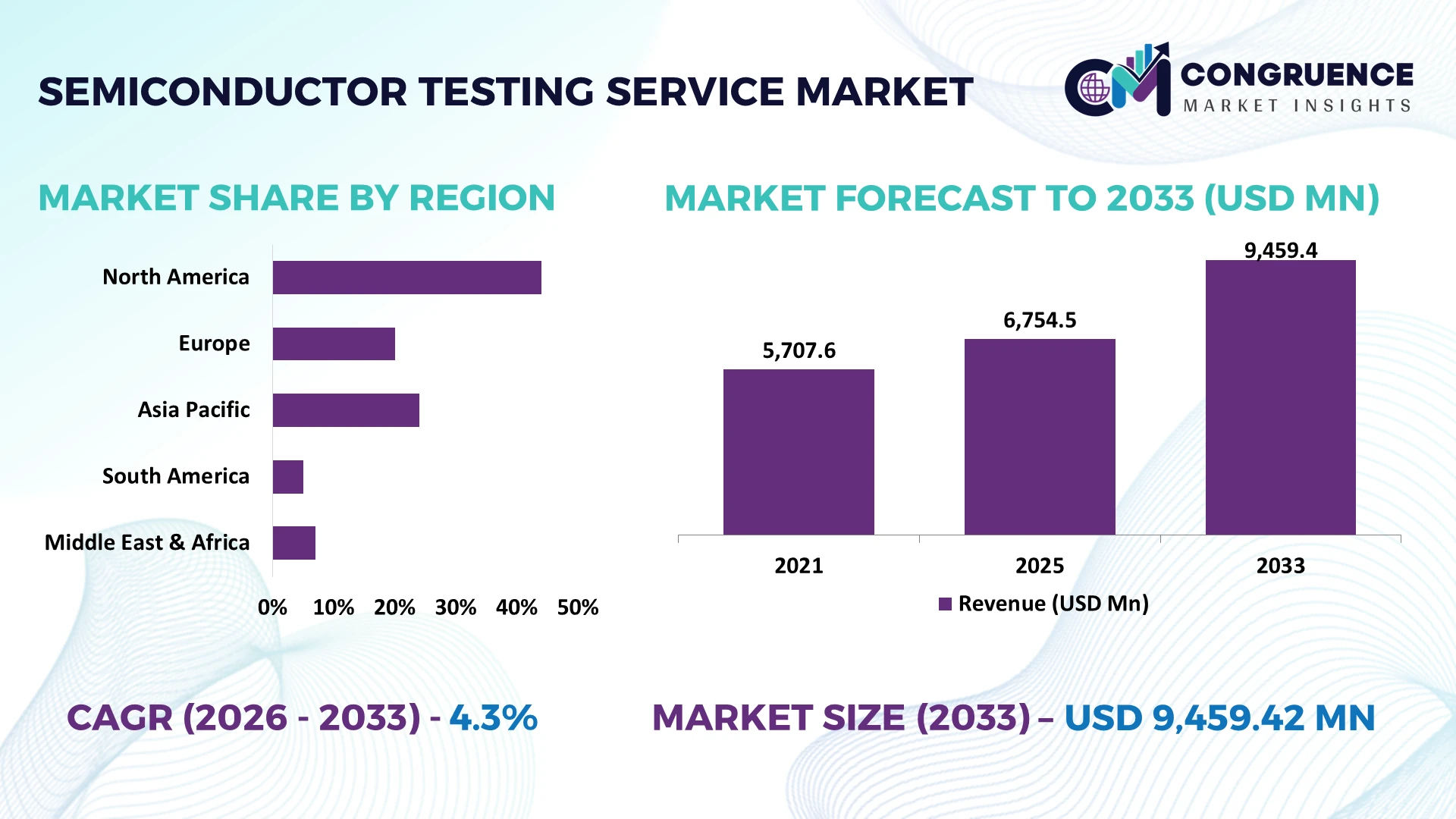
The Global Semiconductor Testing Service Market was valued at USD 6754.45 Million in 2025 and is anticipated to reach a value of USD 9459.42 Million by 2033 expanding at a CAGR of 4.3% between 2026 and 2033. Growth is being driven by rising test insertions for AI accelerators, HBM, chiplets, 2.5D/3D packages, silicon photonics, and automotive power semiconductors as device complexity increases test time and known-good-die requirements.
Taiwan remains the dominant advanced semiconductor testing hub, supported by TSMC’s more than 70% share of global foundry revenue and manufacturing capacity exceeding 17 million 12-inch-equivalent wafers in 2025. ASE is investing NT$108.3 billion in a new Kaohsiung testing cluster. In comparison, Malaysia handles about 13% of global semiconductor testing and packaging, highlighting Taiwan’s deeper concentration in AI, HPC, smartphones, automotive chips, CoWoS, and advanced system validation.
Strategic implication: Testing-service providers positioned close to Taiwan’s advanced packaging ecosystem gain stronger access to high-value AI and HBM workloads, while U.S. CHIPS-backed packaging initiatives accelerate geographic diversification.
Market Size & Growth: USD 6.75 billion in 2025 reaches USD 9.46 billion by 2033 at 4.3%, driven by AI, HBM, and advanced packaging test complexity.
Top Growth Drivers: AI/HPC testing, HBM scaling, and advanced packaging lead demand, while semiconductor test-equipment revenue increased 18% in 2024.
Short-Term Forecast: By 2027, AI-assisted test optimization targets 10–20% lower test time, improving equipment utilization and reducing cost per tested device.
Emerging Technologies: AI-driven adaptive testing, chiplet validation, and silicon-photonics testing are reshaping advanced semiconductor workflows as heterogeneous integration expands.
Regional Leaders: By 2033, modeled demand reaches approximately USD 5.2B in Asia-Pacific, USD 2.1B in North America, and USD 1.2B in Europe, supported by OSAT scale, reshoring, and automotive electronics.
End-User Trends: SoC and memory testers represented roughly 75% of semiconductor test-equipment revenue in 2024 as HPC, custom ASIC, and HBM workloads intensified.
Pilot/Case Example: In 2026, Infineon’s GenAI test-code initiative reduced initial test-module development effort by 20–50%, shifting selected engineering tasks from hours to minutes.
Competitive Landscape: Advantest and Teradyne together controlled over 90% of semiconductor test equipment in 2024, alongside testing ecosystems involving ASE, Amkor, KYEC, and PTI.
Regulatory & ESG Impact: TSMC targets 100% renewable energy by 2040, while U.S. CHIPS programs allocated up to USD 1.6 billion toward advanced-packaging R&D.
Investment & Funding: ASE’s Taiwan Renwu semiconductor testing cluster carries investment exceeding NT$108.3 billion, approximately USD 3.4 billion, strengthening localized AI and advanced-chip testing capacity.
Innovation & Future Outlook: HBM4, 2nm logic, heterogeneous chiplets, and co-packaged optics are shifting testing toward known-good-die validation, high parallelism, and real-time AI analytics.
Semiconductor Testing Service Market demand is concentrating around AI accelerators, HBM memory, advanced logic, automotive electronics, and chiplet-based packages. AI-enabled adaptive testing and automated test-code generation are reducing engineering effort by 20–50%, while U.S.–Asia supply-chain diversification is expanding advanced packaging and validation infrastructure. This shift makes testing capability, automation depth, and proximity to advanced packaging increasingly important strategic differentiators.
Semiconductor testing services are becoming strategically critical as AI accelerators, HBM, chiplets, automotive ICs, and heterogeneous packages increase the cost of shipping defective silicon. Semiconductor test-equipment activity rose 18% in 2024, while SoC and memory testers increased 25%, reflecting higher test insertions for AI/HPC and HBM devices. Supply-chain restructuring is simultaneously pushing testing capacity closer to advanced packaging hubs, reducing dependence on geographically concentrated back-end operations.
AI-assisted test development is changing operating economics. Infineon’s generative-AI test-code implementation reduced initial test-module development effort by roughly 20–50%, compared with conventional engineer-intensive programming. Taiwan combines leading-edge foundry, packaging, and test infrastructure, whereas Malaysia accounts for about 13% of global semiconductor assembly, testing, and packaging activity. This creates distinct strategies: Taiwan concentrates advanced AI/HBM validation, while Malaysia offers scalable outsourced back-end capacity.
Through 2027–2028, higher HBM stack counts, 2nm devices, chiplets, and system-level testing will increase demand for thermal, high-parallelism, and known-good-die validation. ASE’s new Kaohsiung testing cluster, scheduled to start operations in 2027 with over 1,000 jobs, integrates AI inspection and automated guided vehicles. Companies are consequently prioritizing automation, localized ecosystems, and equipment partnerships. Competitive advantage will increasingly depend on test intelligence, yield optimization, and proximity to advanced packaging.
AI computing is structurally increasing semiconductor test intensity as GPUs, custom ASICs, HBM stacks, and advanced packages require additional wafer, memory, thermal, and system-level validation. Semiconductor test-equipment activity increased 18% in 2024, while SoC and memory testers advanced 25% and represented approximately 75% of the segment. Advantest reported that roughly two-thirds of its shipments served computing applications, demonstrating how AI infrastructure is redirecting tester utilization. Higher HBM stack counts and 2.5D/3D integration increase the economic value of identifying defective dies before expensive packaging. Taiwan-based ASE is responding through its Renwu testing cluster, combining wafer and chip testing with AI inspection and factory automation. The strategic shift is clear: test is moving from final quality control toward active yield protection.
Advanced semiconductor testing remains constrained by equipment concentration, high utilization requirements, and dependence on specialized test interfaces. Advantest and Teradyne controlled more than 90% of semiconductor test equipment in 2024, creating procurement exposure for independent OSATs and smaller testing providers. Meanwhile, 97% of Advantest’s first-half FY2024 sales were generated outside Japan, illustrating the cross-border dependency embedded in tester supply chains. Malaysia handles approximately 13% of global assembly, testing, and packaging, but upgrading conventional back-end capacity for HBM and advanced logic requires new handlers, probe cards, thermal control, and engineering expertise. Export controls and semiconductor localization policies further complicate equipment planning. Service providers are mitigating exposure through multi-year procurement, localized component ecosystems, capacity diversification, and partnerships with interface and automation suppliers.
The strongest opportunity lies in converting test data into an active manufacturing optimization layer. AI-assisted programming has already demonstrated 20–50% reductions in initial test-module development effort in Infineon deployments, while SoC and memory test-equipment activity increased 25% in 2024. Malaysia, responsible for approximately 13% of global assembly, testing, and packaging, has an opportunity to move beyond conventional outsourced testing into chiplet, silicon-photonics, and advanced-package validation. Its partnership with Arm also supports a broader transition toward higher-value chip design and engineering capabilities. Through 2027–2028, adaptive test algorithms, predictive yield analytics, and known-good-die screening will become increasingly valuable as HBM4 and heterogeneous packages scale. Testing companies are expanding R&D partnerships and automated facilities, turning accumulated test data into a defensible operational asset rather than a basic service output.
Scaling advanced testing requires engineering capability to keep pace with rapidly changing device architectures. HBM, 2nm logic, chiplets, co-packaged optics, and automotive devices introduce different thermal, signal-integrity, power, and reliability requirements that cannot be addressed through standardized legacy test flows. SoC and memory testers already represent about 75% of semiconductor test-equipment activity, while Teradyne’s semiconductor-test business increased 18.8% in 2025 as AI-compute and system-level demand accelerated. Taiwan’s ASE plans more than 1,000 jobs at its new Renwu testing cluster, underscoring the human-capital requirement even as AI inspection and AGVs automate production. The long-term challenge is therefore not simply equipment availability but scalable test engineering. Providers must invest in workforce development, reusable test software, digital twins, automation, and customer co-development to maintain consistent yield and deployment speed.
System-Level Testing Moves Mainstream: System-level testing is shifting from supplementary screening toward production-critical validation as AI accelerators operate under sustained thermal and power loads. Teradyne’s Titan architecture provides a 30% throughput advantage over conventional batch systems and supports up to 424 parallel test sites. Manufacturers are inserting SLT after wafer and package testing to expose firmware, HBM-interconnect, power-delivery, and thermal faults that conventional ATE can miss, while expanding automated high-density test cells.
Tester Utilization Shifts Toward Compute: Semiconductor test-equipment activity increased 18% in 2024, with SoC and memory testers advancing 25% and representing approximately 75% of activity. Advantest’s computing-related shipments reached roughly two-thirds of its total, reflecting a decisive production shift toward AI accelerators and custom ASICs. Test houses are reallocating engineering resources, floor space, probe capacity, and thermal infrastructure toward high-current compute devices instead of maintaining uniform utilization across legacy applications.
High-Density Automation Reshapes Operations: Automated handlers, machine vision, predictive maintenance, and asynchronous testing are reducing idle time inside high-volume test floors. Teradyne’s Titan supports 320 or 424 sites in the same footprint, provides data rates up to 20 Gbps, and maintains interface reliability beyond 100,000 insertions. Taiwan-based testing operations are increasingly integrating automated material movement and AI inspection, allowing providers to raise equipment utilization without proportionally expanding labor or cleanroom footprints.
Testing Becomes Supply-Chain Insurance: Advanced packaging is changing quality economics because discovering defective chiplets after 2.5D/3D integration destroys substantially more embedded value than rejecting dies earlier. Even 99.5% ATE fault coverage can leave faults undetected in billion-transistor devices, strengthening demand for complementary mission-mode validation. U.S. localization policies and Asian capacity restructuring are prompting OSATs and semiconductor manufacturers to establish geographically diversified qualification flows, dual-site test programs, and closer tester-supplier partnerships.
Package Testing leads with an estimated 35–40% share, supported by its mandatory position between assembly and shipment across logic, memory, analog, RF, and power devices. High-volume parallelism and established ATE infrastructure keep unit economics competitive. Wafer Testing follows as an essential known-good-die screening stage, becoming more valuable as expensive chiplets enter 2.5D/3D packages. Together, wafer and package insertions account for the majority of production testing, while SoC and memory testers represented approximately 75% of test-equipment activity in 2024.
System-Level Testing is the fastest-growing type as AI accelerators, ADAS processors, and heterogeneous devices require validation under realistic software, thermal, and power conditions. Modern SLT platforms deliver around 30% higher throughput than traditional batch architectures and scale to 424 sites. Reliability Testing remains essential for automotive and industrial qualification, while Failure Analysis supports yield learning and root-cause isolation. Providers are consequently shifting investment toward integrated wafer-to-SLT workflows, high-density automation, and advanced thermal management.
Consumer Electronics holds the leading application position at an estimated 28–32% share, reflecting enormous volumes of smartphone, computing, wearable, gaming, and connected-device semiconductors. Mature production flows emphasize parallel testing and low cost per device, while Telecommunications maintains significant demand from RF, networking, 5G, and optical components. Automotive Semiconductors require comparatively intensive reliability screening because ADAS, electrification, and safety-critical electronics impose stringent quality requirements.
Data Centers are the fastest-growing application as GPUs, AI ASICs, HBM, networking silicon, and high-speed interconnect devices raise test complexity. SoC and memory tester activity increased approximately 25% in 2024, while around two-thirds of Advantest shipments served computing applications, illustrating how AI infrastructure is changing equipment allocation. Industrial Electronics remains strategically stable through automation, power electronics, and edge computing. Testing companies are expanding high-current ATE, thermal control, SLT, and high-parallelism capabilities, shifting operational priority from pure device volume toward test intensity and value protected per tested package.
OSAT Providers represent the leading end-user group with an estimated 35–40% share of semiconductor testing service demand because testing is embedded directly within outsourced assembly, packaging, bumping, probing, burn-in, and final-test workflows. Their multi-customer infrastructure generates stronger equipment utilization than captive facilities and supports rapid production scaling. Integrated Device Manufacturers retain substantial internal testing capacity for process control and proprietary devices, while Semiconductor Manufacturers increasingly combine captive test operations with specialist external capacity.
Fabless Companies are the fastest-growing outsourced buyer group as advanced-node AI and custom ASIC developers depend on foundry-OSAT ecosystems rather than owning back-end infrastructure. SoC and memory testers represented roughly 75% of test-equipment activity in 2024, while the two largest ATE suppliers controlled more than 90% of their equipment segment, reinforcing the importance of ecosystem access. Electronics OEMs increasingly influence system-level qualification specifications. Testing providers are responding with customized test programs, engineering co-development, capacity reservations, and integrated package-to-SLT services designed to secure long-duration relationships with high-complexity fabless customers.
Asia-Pacific accounted for the largest market share at approximately 56% in 2025 however, North America is expected to register the fastest growth, expanding at a CAGR of approximately 5.2% between 2026 and 2033.
Advanced Packaging Reshoring Reshapes Testing Capacity
North America represents approximately 22% of semiconductor testing service demand, with the United States concentrating high-value requirements from AI accelerators, data-center processors, automotive electronics, aerospace, and advanced logic. Domestic testing infrastructure is shifting from predominantly captive and offshore-dependent models toward integrated wafer-fabrication, packaging, and final-test ecosystems. Arizona is emerging as the pivotal deployment cluster because TSMC’s manufacturing footprint is being complemented by Amkor’s advanced packaging and test expansion. Amkor’s Peoria campus is planned with more than 750,000 square feet of cleanroom space across two phases and capacity supporting high-volume AI and HPC devices. Apple and NVIDIA-linked production requirements further strengthen utilization prospects. Companies are responding to supply-chain security priorities through local qualification, automated test cells, advanced 2.5D validation, and closer foundry-OSAT coordination.
United States Market Outlook: Arizona is becoming the country’s strongest end-to-end semiconductor manufacturing and test corridor. Amkor’s Peoria operation is designed to process approximately 14,500 wafers and 3.7 million assembled-and-tested units monthly under earlier capacity specifications. Production ramping from 2028 will strengthen domestic testing availability for AI, communications, automotive, and advanced computing devices while reducing reliance on Asian back-end processing.
Automotive Electronics Anchor Testing Modernization
Europe accounts for approximately 14% of semiconductor testing service activity, with demand concentrated around automotive ICs, industrial automation, power semiconductors, sensors, and secure electronics. Germany, France, Italy, and the Netherlands anchor the ecosystem, but Germany carries the strongest production-linked testing intensity through automotive and industrial semiconductor manufacturing. European Chips Act initiatives are encouraging localized production and qualification as manufacturers reduce exposure to external supply disruptions. Infineon opened its Dresden Smart Power Fab in July 2026 following a €5 billion investment, creating approximately 1,000 direct jobs and expanding capacity for analog, mixed-signal, and power devices. This manufacturing expansion creates downstream requirements for wafer probing, reliability qualification, power-device characterization, and failure analysis. Testing providers are aligning capabilities with silicon-carbide, automotive safety, industrial power-management, and energy-efficient data-center applications rather than competing primarily on high-volume consumer-device testing.
Germany Market Outlook: Dresden’s semiconductor cluster gives Germany a differentiated testing position centered on automotive, industrial, and power electronics rather than smartphone-scale volumes. Infineon’s new facility can ramp production capacity at roughly twice the conventional expansion pace when required. Local test engineering increasingly emphasizes high-voltage characterization, thermal reliability, functional safety, and long-lifecycle qualification, strengthening Germany’s role in mission-critical semiconductor validation.
Back-End Scale Meets Advanced AI Testing
Asia-Pacific commands approximately 56% of global semiconductor testing service activity, supported by dense foundry, OSAT, memory, electronics, and substrate ecosystems across Taiwan, China, South Korea, Malaysia, Singapore, Japan, and increasingly India. Taiwan alone historically represented about 42% of leading outsourced IC packaging and testing activity through companies including ASE, PTI, KYEC, ChipMOS, and Chipbond. The operating mix is now moving toward HBM, AI accelerators, chiplets, and 2.5D/3D integration, increasing requirements for wafer sort, known-good-die screening, thermal testing, and system-level validation. Singapore is adding dedicated HBM advanced-packaging capacity, while Micron’s Sanand facility positions India as a new high-volume assembly-and-test node. The Sanand operation expects tens of millions of chips during 2026 and hundreds of millions in 2027, demonstrating how companies are geographically diversifying Asian back-end capacity.
Taiwan Market Outlook: Taiwan remains the strategically strongest testing ecosystem because leading-edge foundry production sits beside mature OSAT, substrate, probe-card, and equipment infrastructure. Five Taiwanese companies historically represented approximately 42% of major outsourced packaging and testing activity. ASE’s continuing capacity expansion reinforces Taiwan’s advantage in AI/HBM validation, where proximity between wafer fabrication, advanced packaging, and testing shortens qualification cycles and protects expensive packaged-device yields.
Localization Targets Electronics Supply Resilience
South America represents approximately 3% of semiconductor testing service demand, with Brazil providing the region’s most developed semiconductor back-end and electronics-manufacturing base. Demand remains concentrated in consumer electronics, telecommunications equipment, automotive systems, payment devices, industrial controls, and connected infrastructure rather than leading-edge AI processors. Brazil’s established packaging and testing capabilities around São Paulo and Rio Grande do Sul provide a foundation for localization, although limited advanced wafer fabrication and dependence on imported equipment restrict deployment scale. HT Micron’s São Leopoldo operations demonstrate the region’s practical capability in memory packaging, multi-chip integration, and semiconductor testing, supported by domestic development institutions. Brazil has also used industrial policy and financing mechanisms to strengthen semiconductor production. Providers are prioritizing localized qualification, memory-device testing, automotive electronics, and partnerships with universities and electronics manufacturers instead of replicating Asia’s capital-intensive advanced-node model.
Brazil Market Outlook: Brazil offers South America’s clearest semiconductor testing pathway through existing electronics demand and domestic back-end capabilities. BNDES previously approved R$99 million for HT Micron to expand production capacity and develop next-generation memory components. The strategic advantage lies in serving locally manufactured smartphones, connected devices, vehicles, and industrial electronics with shorter qualification chains while progressively building higher-value packaging and test engineering expertise.
National Technology Programs Build New Ecosystems
Middle East & Africa accounts for approximately 5% of semiconductor testing service demand, with current activity weighted toward imported devices, telecommunications, defense electronics, data centers, automotive systems, and industrial infrastructure. Saudi Arabia and the UAE are shifting the landscape through sovereign-backed AI infrastructure and semiconductor ecosystem programs, although commercial testing capacity remains considerably below established Asian hubs. Saudi Arabia’s National Semiconductor Hub targets 50 semiconductor design companies and 5,000 trained IC engineers by 2030, creating a future pipeline for prototype validation, characterization, and outsourced testing. Ten international semiconductor companies were preparing Riyadh operations during 2025, demonstrating early ecosystem formation. Instead of immediately pursuing high-volume commodity testing, companies are entering through fabless design, edge-AI devices, research partnerships, and specialized validation. This creates an emerging testing requirement around prototype qualification and low-to-medium-volume advanced devices.
Saudi Arabia Market Outlook: Saudi Arabia holds the strongest strategic momentum through the National Semiconductor Hub, KACST, KAUST, and technology localization programs. The initiative targets 50 chip-design companies, 25 international semiconductor experts, and 5,000 engineers. As local tape-outs and fabless operations increase, demand will shift toward engineering test, characterization, reliability validation, and partner-based overseas production qualification before large-scale domestic back-end infrastructure becomes economically justified.
ASE Technology, Amkor Technology, JCET Group, Tongfu Microelectronics, Powertech Technology and specialist test houses such as KYEC compete across outsourced semiconductor validation, with global OSAT leaders challenging Taiwan- and China-based capacity specialists on advanced packaging integration. The top five outsourced packaging-and-test groups represent approximately 75% of established industry activity, creating meaningful scale barriers. Competition increasingly centers on AI/HBM capability, where high-density automation can improve throughput by around 20–30%, while integrated wafer-to-system-level workflows can shorten qualification cycles by 10–20%. ASE and Amkor are expanding advanced test campuses; JCET and Tongfu leverage Chinese manufacturing ecosystems; KYEC emphasizes high-end logic and AI testing. The competitive shift is moving from low-cost final test toward thermal control, known-good-die screening, system-level validation and data-driven yield optimization. Capital-intensive ATE, engineering talent and customer qualification remain major entry barriers. Winning requires advanced-node expertise, consistently high utilization, rapid engineering turnaround, geographic resilience and tightly integrated customer partnerships across global supply chains.
ASE Technology Holding Co., Ltd.
Amkor Technology, Inc.
JCET Group Co., Ltd.
Tongfu Microelectronics Co., Ltd.
Powertech Technology Inc.
King Yuan Electronics Co., Ltd. (KYEC)
Tianshui Huatian Technology Co., Ltd.
ChipMOS Technologies Inc.
Chipbond Technology Corporation
UTAC Holdings Ltd.
Hana Micron Inc.
Unisem (M) Berhad
Carsem (M) Sdn. Bhd.
Current semiconductor testing is moving from fixed-sequence ATE toward AI-assisted adaptive testing, high-parallelism system-level testing, and real-time analytics. Infineon’s GenAI test engineering has reduced initial test-module development effort by 20–50%, while Teradyne’s asynchronous Titan architecture delivers about 30% higher throughput than traditional batch systems. High-volume deployment is expanding across wafer sort, final test, and SLT, giving OSATs and IDMs faster qualification, higher equipment utilization, and lower cost per device.
Emerging technology centers on chiplet-aware validation, HBM testing, digital twins, active thermal control, and data-driven yield optimization. Modern SLT systems support up to 424 test sites and 20 Gbps data rates, while AI infrastructures increasingly optimize test flows in real time. Compared with legacy batch testing, asynchronous platforms improve throughput by roughly 30%, creating an advantage for providers handling AI accelerators, advanced memory, and heterogeneous packages where test intensity and thermal complexity are highest.
From 2026–2028, disruptive adoption will concentrate on autonomous test decisioning, silicon-photonics validation, predictive maintenance, and virtual test-program development. Providers integrating ATE, analytics, wafer-level data, and system-level results will shorten ramp cycles and protect expensive packaged devices. Companies acting now gain customer lock-in, better yield intelligence, and scalable capacity before advanced packaging makes fragmented testing workflows operationally uncompetitive.
December 2024 — Amkor Technology secured a finalized U.S. CHIPS award supporting its Arizona advanced packaging and test facility, expected to create over 4,000 jobs. The project localizes back-end capability for AI and HPC chips, strengthening supply resilience. Source: commerce.gov
February 2025 — ASE Technology opened its fifth Penang plant, expanding floor space from 1.0 million to 3.4 million square feet. The expansion scales advanced packaging and testing capacity while embedding Industry 4.0 automation for next-generation semiconductor production. Source: aseglobal.com
October 2025 — Advantest integrated NVIDIA machine-learning technology with ACS Real-Time Data Infrastructure for high-volume semiconductor testing. NVIDIA selected the platform for Blackwell devices, shifting workflows from delayed analysis toward adaptive, real-time yield optimization and lower testing latency. Source: advantest.com
March 2026 — Infineon’s GenAI for Test Engineering deployment reduced manual effort for initial test-module creation by 20–50%, with selected modules generated in minutes instead of hours. The workflow improves engineering scalability, code consistency, reuse and development speed. Source: porsche-consulting.com
The Semiconductor Testing Service Market report evaluates testing demand across Wafer Testing, Package Testing, System-Level Testing, Reliability Testing, and Failure Analysis, with application coverage spanning automotive semiconductors, consumer electronics, telecommunications, industrial electronics, and data centers. It also assesses Semiconductor Manufacturers, Fabless Companies, Integrated Device Manufacturers, OSAT Providers, and Electronics OEMs across North America, Europe, Asia-Pacific, South America, and the Middle East & Africa.
The analysis tracks advanced ATE, AI-assisted adaptive testing, HBM validation, chiplet testing, active thermal control, digital twins, and automated system-level testing. With semiconductor test-equipment activity rising sharply as AI and HBM increase test intensity, the report examines capacity localization, outsourced testing models, qualification requirements, and packaging integration. Between 2026 and 2033, these insights support investment planning, expansion, partnership selection, competitive benchmarking, technology prioritization, and identification of emerging testing opportunities linked to AI infrastructure and heterogeneous integration.
| Report Attribute/Metric | Report Details |
|---|---|
Market Revenue in 2025 | USD 6754.45 Million |
Market Revenue in 2033 | USD 9459.42 Million |
CAGR (2026 - 2033) | 4.3% |
Base Year | 2025 |
Forecast Period | 2026 - 2033 |
Historic Period | 2021 - 2025 |
Segments Covered | By Type
By Application
By End-User
|
Key Report Deliverable | Revenue Forecast, Growth Trends, Market Dynamics, Segmental Overview, Regional and Country-wise Analysis, Competition Landscape |
Region Covered | North America, Europe, Asia-Pacific, South America, Middle East, Africa |
Key Players Analyzed | ASE Technology Holding Co., Ltd., Amkor Technology, Inc., JCET Group Co., Ltd., Tongfu Microelectronics Co., Ltd., Powertech Technology Inc., King Yuan Electronics Co., Ltd. (KYEC), Tianshui Huatian Technology Co., Ltd., ChipMOS Technologies Inc., Chipbond Technology Corporation, UTAC Holdings Ltd., Hana Micron Inc., Unisem (M) Berhad, Carsem (M) Sdn. Bhd. |
Customization & Pricing | Available on Request (10% Customization is Free) |