
Reports
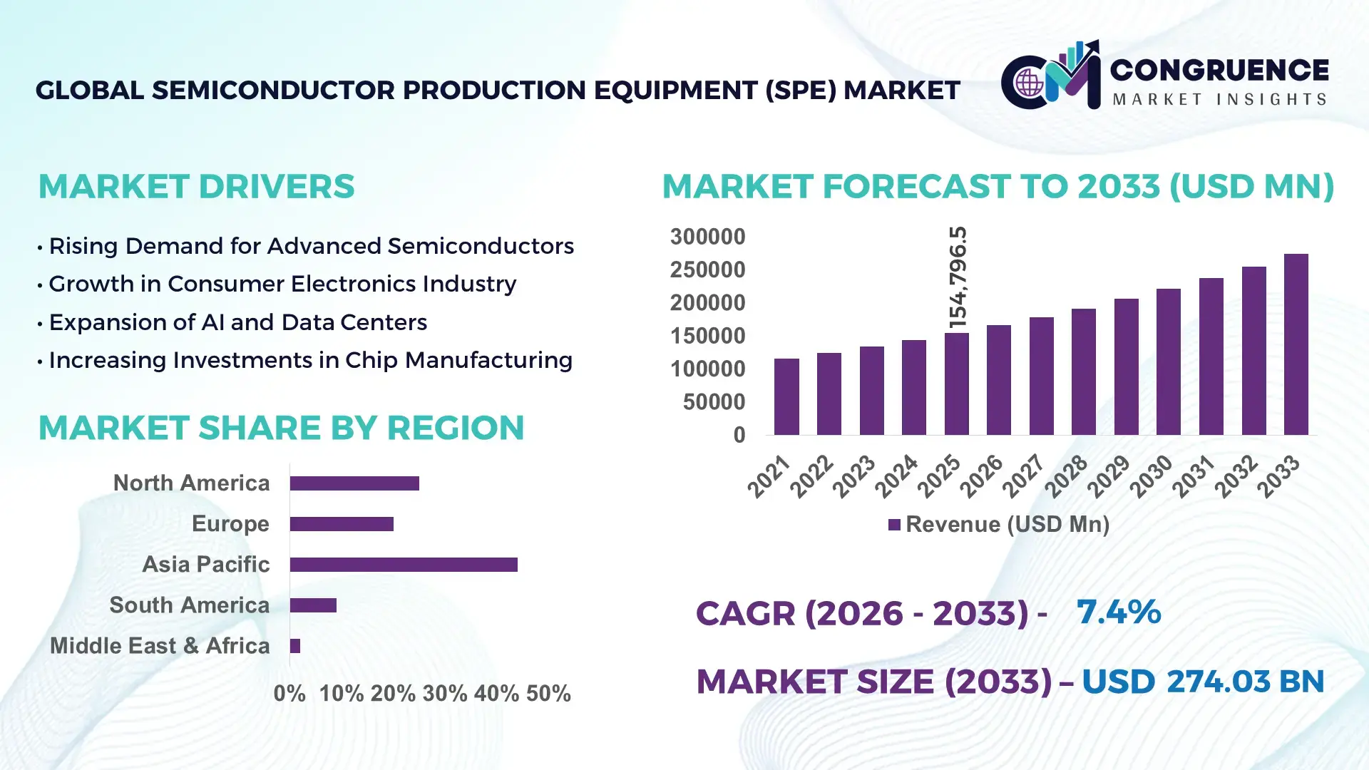
The Global Semiconductor Production Equipment (SPE) Market was valued at USD 154796.47 Million in 2025 and is anticipated to reach a value of USD 274028 Million by 2033 expanding at a CAGR of 7.4% between 2026 and 2033.
Advanced node transitions below 5nm and the rapid expansion of AI-driven chip fabrication are accelerating capital expenditure cycles, with lithography and etching equipment demand rising by over 18% compared to mature-node tools. Between 2024 and 2026, geopolitical realignment of semiconductor supply chains, particularly driven by U.S.–China trade restrictions and incentive programs like the CHIPS Act, has reshaped equipment sourcing and localized manufacturing strategies across Asia and North America.
China dominates capacity expansion with over 32% of global wafer fab investments, supported by aggressive domestic funding exceeding USD 40 billion annually, while Taiwan contributes nearly 20% of advanced-node output, led by sub-5nm production scaling. South Korea accounts for approximately 17% of memory-focused equipment demand, driven by high-bandwidth memory (HBM) deployment for AI servers. Compared to Europe’s sub-10% share, Asia-Pacific’s combined dominance exceeds 70%, reflecting concentrated manufacturing ecosystems and faster technology adoption cycles.
This concentration of capacity and capital signals that strategic partnerships and regional diversification are now critical for equipment vendors aiming to secure long-term contracts and mitigate geopolitical risk exposure.
Market Size & Growth: USD 154,796.47M (2025) to USD 274,028M (2033), 7.4% CAGR, driven by AI chip fabrication and advanced-node scaling.
Top Growth Drivers: EUV adoption +22%, AI chip demand +19%, regional fab investments +25%.
Short-Term Forecast: By 2027, wafer throughput efficiency improves by 15% due to automation integration.
Emerging Technologies: AI-driven process control, EUV lithography, and advanced materials boost yield rates by 12–18%.
Regional Leaders: Asia-Pacific USD 180B+, North America USD 55B+, Europe USD 30B; all driven by localized supply chain expansion.
Consumer/End-User Trends: AI and data center chip demand accounts for over 35% of new equipment deployment.
Pilot/Case Example: 2025 fab automation project improved defect detection accuracy by 28% and reduced downtime by 20%.
Competitive Landscape: Top player holds ~18% share; key players include Applied Materials, ASML, Lam Research, Tokyo Electron.
Regulatory & ESG Impact: Energy-efficient fabs reduce power usage by 14%, aligned with stricter emission norms in 2025.
Investment & Funding: Over USD 120B global fab investments driven by public-private partnerships and national incentives.
Innovation & Future Outlook: Transition to sub-3nm nodes and heterogeneous integration enhances performance efficiency by 20%.
Logic and foundry applications contribute approximately 48% of total equipment demand, followed by memory manufacturing at 32%, while packaging and testing account for 20%, reflecting increasing complexity in chip architectures. Innovations such as high-NA EUV systems and AI-enabled predictive maintenance are improving yield by over 15%. Asia-Pacific continues to dominate with over 70% demand share, supported by localized supply chain strategies amid ongoing geopolitical shifts. The growing focus on heterogeneous integration signals a transition toward more flexible, high-performance semiconductor ecosystems, setting the stage for strategic capacity alignment.
Semiconductor production equipment is rapidly transforming into a strategic control point for global technology leadership, as advanced chip manufacturing defines competitiveness across AI, automotive, and defense sectors. Equipment intensity per wafer has increased by over 25% with sub-5nm scaling, forcing manufacturers to prioritize precision, automation, and throughput optimization. The market is accelerating as fabs shift toward high-mix, high-performance production environments, where tool capability directly determines yield and profitability.
Supply chain restructuring and export controls are shifting procurement strategies, pushing localized equipment ecosystems and dual-sourcing models. High-NA EUV lithography improves patterning efficiency by 30% while reducing defect-related costs by 18% compared to legacy deep ultraviolet systems. Asia-Pacific leads in production volume with over 70% share, while North America leads in innovation adoption with nearly 40% penetration in AI-driven process control systems. Over the next 2–3 years, fab automation is expected to increase throughput efficiency by 15%, directly enhancing output consistency.
Sustainability is becoming a competitive lever, with energy-efficient equipment reducing fab power consumption by 14%, translating into both regulatory compliance and operational savings. A 2025 deployment of AI-based inspection systems improved defect detection rates by 28%, minimizing yield losses. Equipment manufacturers are shifting capital allocation toward advanced-node R&D and regional expansion, signaling a decisive move toward technology leadership. Companies that optimize integration, localization, and efficiency will secure long-term competitive advantage in an increasingly consolidated and performance-driven ecosystem.
The transition toward sub-5nm and AI-specific chip architectures is forcing a fundamental expansion in semiconductor production equipment demand, driven by increased process complexity and higher tool intensity per wafer. Advanced-node manufacturing requires nearly 35% more processing steps compared to mature nodes, directly increasing reliance on deposition, etching, and lithography systems. Simultaneously, AI chip demand has surged by over 20%, accelerating the need for high-performance fabrication capabilities. A major global trigger is the ongoing supply chain restructuring, where governments are incentivizing domestic fabrication, leading to over 25% growth in regional fab investments across North America and Asia. This shift is forcing equipment manufacturers to scale production capacity and localize supply chains. In response, companies are accelerating capital investments, forming strategic partnerships with foundries, and expanding manufacturing footprints near key semiconductor hubs to secure long-term contracts and reduce delivery lead times.
The semiconductor production equipment market is constrained by high capital intensity, supply chain concentration, and raw material dependencies, particularly in critical components such as precision optics and rare materials. Equipment costs have increased by nearly 18% due to inflation in specialized components, while lead times have extended by over 20% due to supply bottlenecks. A key real-world constraint is the concentration of advanced lithography component manufacturing within a limited supplier base, creating systemic risks and limiting scalability. These constraints directly impact production timelines, delay fab commissioning, and increase overall project costs. Companies are mitigating these risks by diversifying supplier networks, entering long-term procurement agreements, and investing in alternative material technologies. Additionally, some manufacturers are redesigning equipment architectures to reduce dependency on constrained components, enabling more flexible and resilient production strategies.
High-impact opportunities are emerging in next-generation technologies such as high-NA EUV, heterogeneous integration, and AI-driven process optimization, which are reshaping production efficiency and performance benchmarks. High-NA EUV systems improve resolution capability by over 40%, enabling further node miniaturization, while AI-driven predictive maintenance reduces downtime by nearly 25%. An important future signal is the rapid expansion of advanced packaging, which is expected to account for over 30% of total semiconductor value creation, creating new demand for specialized equipment. Additionally, emerging markets in Southeast Asia are witnessing over 20% growth in fab investments, offering new geographic expansion opportunities. Companies are positioning for dominance by increasing R&D spending, forming ecosystem partnerships with chipmakers, and investing in modular equipment platforms that support flexible manufacturing. This strategic shift is unlocking new revenue streams and strengthening competitive positioning in high-growth segments.
Execution challenges in the semiconductor production equipment market are intensifying due to infrastructure limitations, rising energy demands, and increasing technological complexity. Advanced fabs require up to 30% more energy consumption, placing pressure on grid infrastructure and increasing operational costs. Additionally, integration complexity across multi-layer processes has increased defect risks by nearly 15%, impacting yield consistency. A significant real-world pressure is the limitation of skilled labor and technical expertise required to operate advanced equipment, slowing adoption and scaling efforts. These challenges directly affect long-term growth sustainability and profitability. To remain competitive, companies must invest heavily in workforce training, develop energy-efficient equipment solutions, and enhance system interoperability. Strategic collaborations with governments and technology partners are becoming essential to address infrastructure gaps and ensure scalable, resilient growth in an increasingly demanding production environment.
The Semiconductor Production Equipment (SPE) Market is segmented across equipment types, applications, and end-user industries, reflecting highly specialized demand distribution. Lithography, etching, and deposition tools dominate core fabrication processes, while inspection and cleaning systems are gaining traction due to rising yield sensitivity. Wafer fabrication accounts for over 50% of total equipment deployment, followed by packaging and testing as chip complexity increases. Demand is shifting toward advanced-node manufacturing and heterogeneous integration, driving higher adoption of precision equipment. End-user demand remains concentrated in semiconductor manufacturing, contributing nearly 60%, while automotive and telecommunications segments are accelerating due to AI and connectivity requirements. This segmentation highlights a clear transition toward high-performance, efficiency-driven equipment deployment, influencing investment priorities and product innovation strategies.
Lithography equipment dominates the market with approximately 32% share, driven by its critical role in defining chip architecture and enabling advanced-node scaling. Its structural dominance stems from unmatched precision and integration capability in sub-5nm manufacturing. However, inspection and metrology equipment is emerging as the fastest-growing segment, expanding at over 14% due to rising yield sensitivity and defect detection requirements in complex chip designs. Compared to lithography, which defines structure, inspection systems are increasingly critical in maintaining production efficiency and minimizing costly defects, creating a shift in investment focus.
Etching and deposition equipment collectively account for nearly 45% of the market, forming the backbone of material layering and pattern transfer processes. Cleaning equipment holds a smaller but strategic share of around 10%, ensuring contamination-free environments essential for advanced nodes. Demand is shifting toward integrated solutions combining etching, deposition, and inspection capabilities, forcing companies to innovate modular and high-precision systems. Equipment manufacturers are expanding production capacity and prioritizing R&D in metrology and hybrid tool platforms, signaling a gradual shift from pure fabrication tools to yield-optimization technologies.
“According to a 2025 report by SEMI, advanced inspection and metrology equipment was adopted by over 65% of leading semiconductor fabs, resulting in a 20% improvement in defect detection accuracy, reinforcing its growing strategic importance.”
Wafer fabrication leads the application segment with over 52% share, driven by its central role in chip production and high equipment intensity per wafer. This concentration exists due to the complexity of advanced-node processes requiring multiple precision steps. Assembly and packaging is the fastest-growing segment, expanding by nearly 16% as heterogeneous integration and chiplet architectures gain traction, increasing demand for advanced packaging solutions. Compared to wafer fabrication’s scale-driven dominance, packaging is emerging as a high-value segment enabling performance optimization.
Testing and inspection, along with memory and logic device manufacturing, collectively contribute around 48% of demand. Memory devices continue to require high-volume, standardized equipment, while logic devices are shifting toward customized, high-performance solutions. Companies are adapting by scaling packaging capabilities and integrating testing systems closer to production lines to reduce latency. This shift highlights a movement toward end-to-end optimization, where packaging and testing are becoming as critical as fabrication in determining overall chip performance and yield.
“According to a 2025 report by SEMI, advanced packaging solutions were deployed across over 1,200 semiconductor facilities, improving output efficiency by 18%, highlighting its rapid operational adoption.”
Semiconductor manufacturing dominates the end-user segment with approximately 58% share, reflecting its direct dependency on high-performance equipment for chip production. This dominance is driven by continuous node advancement and increasing fabrication complexity. The automotive industry is the fastest-growing segment, expanding by over 15% due to rising demand for electric vehicles and advanced driver-assistance systems requiring high-performance chips. Compared to the established semiconductor manufacturing base, automotive demand is more application-specific and rapidly evolving.
The electronics and consumer electronics sectors, along with telecommunications, collectively account for around 42% of demand, driven by high-volume device production and connectivity expansion. Telecommunications is witnessing accelerated adoption due to 5G infrastructure deployment, while consumer electronics demand remains stable but volume-driven. Companies are targeting these segments through customized equipment solutions, flexible pricing models, and strategic partnerships with OEMs. This shift indicates a transition toward diversified demand sources, where non-traditional sectors are increasingly influencing equipment innovation and procurement strategies.
“According to a 2025 report by SEMI, adoption among automotive semiconductor manufacturers increased by 22%, with over 300 companies implementing advanced fabrication solutions, leading to a 17% improvement in production efficiency, indicating a strong shift in demand dynamics.”
Asia-Pacific accounted for the largest market share at 71% in 2025 however, North America is expected to register the fastest growth, expanding at a CAGR of 8.2% between 2026 and 2033.
Asia-Pacific dominates production volume and equipment deployment due to concentrated fabrication ecosystems, while North America is accelerating through advanced-node innovation and domestic capacity expansion. Europe holds approximately 9% share, leading in precision engineering and sustainability-driven equipment adoption. A key structural shift is the global supply chain realignment driven by policy incentives and export controls, pushing localized manufacturing across regions. Demand remains concentrated in Asia-Pacific, innovation leadership is strengthening in North America, and regulatory-driven efficiency is shaping Europe. Companies are increasingly balancing regional scale with localized investment strategies to secure long-term competitive positioning.
How is advanced fabrication demand reshaping equipment deployment strategies?
North America accounts for nearly 16% of global demand, driven by high-performance computing, AI chips, and defense-related semiconductor requirements. A major structural force is policy-driven localization, with domestic incentives accelerating fab investments by over 28%. Execution is shifting toward AI-enabled process control and automation, improving production efficiency by 15%. Equipment suppliers are expanding regional manufacturing capacity, with over 20% increase in localized tool assembly. Enterprises prioritize high-precision, innovation-led solutions over cost, favoring long-term performance gains. This region is attracting strategic investments due to its focus on advanced-node leadership and technology sovereignty, making it critical for companies targeting innovation-driven growth.
What forces are driving precision-focused equipment adoption and compliance shifts?
Europe contributes approximately 9% of the global market, with Germany and the Netherlands leading due to strong semiconductor equipment engineering capabilities. Regulatory pressure around energy efficiency and emissions is a key force, pushing fabs to adopt equipment that reduces energy consumption by over 14%. Operational shifts include integration of sustainable manufacturing processes and precision metrology systems. Equipment deployment is increasingly aligned with compliance standards, improving efficiency by 12%. Enterprises exhibit a quality-first, compliance-driven purchasing behavior, prioritizing reliability over scale. This region forces companies to innovate in energy-efficient and precision-driven equipment, shaping long-term product development strategies.
What is enabling rapid scaling and high-volume equipment deployment?
Asia-Pacific leads with over 71% market share, driven by manufacturing hubs in China, Taiwan, South Korea, and Japan. The region benefits from strong supply chain integration and cost-efficient production infrastructure, enabling large-scale equipment deployment. Execution-level shifts include rapid adoption of advanced-node tools and localized manufacturing, with over 30% increase in domestic equipment production. Companies are expanding fab capacity by nearly 25% to meet rising demand for AI and consumer electronics chips. Enterprises prioritize scale and speed, optimizing throughput and cost efficiency. This region remains critical for global expansion strategies due to its unmatched production scale and accelerating demand.
What limits scaling while shaping localized demand patterns?
South America holds a modest 2% market share, with Brazil leading regional demand driven by electronics manufacturing and automotive applications. Infrastructure limitations and high import dependency constrain growth, increasing equipment costs by nearly 18%. However, localized demand is rising, with adoption increasing by 12% in assembly and testing operations. Companies are focusing on smaller-scale deployments and strategic partnerships to overcome supply constraints. Enterprises exhibit strong price sensitivity, prioritizing cost-effective solutions over advanced capabilities. This region presents a balanced opportunity, where targeted investment can unlock growth, but scalability challenges require cautious strategic planning.
How are infrastructure investments reshaping equipment demand dynamics?
The Middle East & Africa region contributes approximately 2% of global demand, driven by infrastructure modernization and digital transformation initiatives in countries such as the UAE and Saudi Arabia. Investment-led transformation is accelerating adoption, with technology deployment increasing by 15% in key industrial zones. Execution shifts include integration of semiconductor capabilities within broader industrial and smart city projects. Strategic partnerships and government-backed initiatives are enabling equipment deployment growth of over 10%. Enterprises focus on long-term infrastructure value rather than immediate scale. This region is emerging as a strategic expansion zone, where early investment positions companies for future demand growth.
China – 32% share: Semiconductor Production Equipment (SPE) Market dominance driven by aggressive domestic fab expansion and government-backed manufacturing investments.
Taiwan – 20% share: Semiconductor Production Equipment (SPE) Market leadership supported by advanced-node production capacity and strong foundry ecosystem.
The Semiconductor Production Equipment (SPE) Market is defined by intense competition between global technology leaders such as Applied Materials, ASML, Lam Research, Tokyo Electron, and KLA, alongside emerging regional players focusing on cost optimization and localized supply. The top five players collectively control approximately 68% of the market, competing primarily on technology precision, process efficiency, and supply chain reliability. Technology leadership drives differentiation, with advanced-node tools delivering up to 30% higher efficiency, while cost-focused players compete with 15% lower pricing in mature-node segments.
Competition is increasingly execution-driven, with companies expanding regional manufacturing, forming strategic partnerships with fabs, and investing heavily in R&D for next-generation equipment. A key competitive shift is the move toward vertical integration and service-based models, enabling stronger customer lock-in and recurring revenue streams. High entry barriers persist due to capital intensity, technological complexity, and supply chain dependencies. To win, companies must combine innovation leadership, localized production, and integrated service capabilities to outperform both global incumbents and agile regional challengers.
Applied Materials
ASML
Lam Research
Tokyo Electron
KLA Corporation
Hitachi High-Tech Corporation
SCREEN Holdings
Advantest Corporation
ASM International
Nikon Corporation
Canon Inc.
Teradyne Inc.
Advanced lithography and precision process control systems are currently defining operational performance, with EUV lithography improving patterning accuracy by 30% and increasing wafer yield by 18%. Adoption has crossed 55% in leading-edge fabs, driven by sub-5nm requirements. Integration of AI-based process control is reducing defect rates by 20%, directly optimizing throughput and lowering rework costs, giving early adopters a measurable production advantage. Emerging technologies such as high-NA EUV and atomic layer deposition (ALD) are accelerating capability expansion, with ALD improving material uniformity by 25% while reducing material waste by 15%. Deployment of advanced metrology systems has reached nearly 60% in high-performance fabs, enabling real-time defect detection. This shift is transforming fabrication into a data-driven environment, where precision and predictability directly influence profitability and cycle time reduction.
Disruptive integration of AI-driven predictive maintenance and digital twin modeling is redefining equipment lifecycle management, reducing downtime by 22% and maintenance costs by 17%. Compared to legacy reactive maintenance systems, predictive models improve operational uptime by over 25%. Equipment leaders benefit from this transition through service-based revenue models, while fabs gain cost predictability and performance stability. Between 2026 and 2028, integrated smart-fab ecosystems are expected to dominate, with over 65% of advanced facilities deploying interconnected equipment platforms. Companies investing in AI integration, modular tool design, and high-precision systems are securing long-term competitive positioning as technology becomes the primary differentiator in production efficiency and scalability.
March 2026 – ASML launched next-generation High-NA EUV systems, achieving 35% higher resolution and enabling sub-2nm chip production. This innovation strengthens advanced-node leadership and accelerates adoption among leading fabs. [Next-Gen Lithography]
Source: https://www.asml.com
November 2025 – Applied Materials expanded U.S. manufacturing capacity, increasing production output by 20% to support localized semiconductor supply chains. This move enhances delivery timelines and reduces dependency on offshore manufacturing. [Capacity Expansion]
Source: https://www.appliedmaterials.com
July 2025 – Lam Research partnered with a major foundry to deploy AI-driven etching systems, improving process precision by 18% and reducing defects significantly. This collaboration enhances yield optimization and strengthens long-term customer integration. [AI Integration Shift]
Source: https://www.lamresearch.com
January 2024 – Tokyo Electron introduced advanced deposition technology, improving film uniformity by 22% and boosting production efficiency. This development supports next-generation chip architectures and reinforces competitive positioning in material engineering. [Process Innovation]
Source: https://www.tel.com
This report delivers comprehensive coverage of the Semiconductor Production Equipment (SPE) Market by analyzing five core equipment types, five application segments, and five end-user industries across five major regions. It captures detailed insights into lithography, etching, deposition, cleaning, and metrology systems, alongside key applications such as wafer fabrication and advanced packaging. Geographic analysis spans Asia-Pacific, North America, Europe, South America, and Middle East & Africa, reflecting over 90% of global semiconductor manufacturing activity. The report also incorporates emerging technologies including AI-driven process control, high-NA EUV systems, and heterogeneous integration platforms.
Analytical depth is reinforced through evaluation of over 25 segment-level dynamics and profiling of 10+ leading equipment manufacturers, supported by adoption benchmarks such as 60% deployment of advanced metrology systems and 55% penetration of EUV tools in leading-edge fabs. It highlights demand distribution shifts, with over 70% concentration in high-performance fabrication environments and increasing adoption of automation exceeding 45% across advanced facilities.
Strategically, the report supports investment prioritization, regional expansion planning, and competitive positioning by identifying high-impact growth zones, technology adoption trends, and operational efficiency benchmarks. It also outlines forward-looking developments between 2026 and 2033, enabling decision-makers to align with evolving production models and capture emerging opportunities in next-generation semiconductor manufacturing ecosystems.
| Report Attribute/Metric | Report Details |
|---|---|
|
Market Revenue in 2025 |
USD 154796.47 Million |
|
Market Revenue in 2033 |
USD 274028 Million |
|
CAGR (2026 - 2033) |
7.4% |
|
Base Year |
2025 |
|
Forecast Period |
2026 - 2033 |
|
Historic Period |
2021 - 2025 |
|
Segments Covered |
By Type
By Application
By End-User
|
|
Key Report Deliverable |
Revenue Forecast, Growth Trends, Market Dynamics, Segmental Overview, Regional and Country-wise Analysis, Competition Landscape |
|
Region Covered |
North America, Europe, Asia-Pacific, South America, Middle East, Africa |
|
Key Players Analyzed |
Applied Materials, ASML, Lam Research, Tokyo Electron, KLA Corporation, Hitachi High-Tech Corporation, SCREEN Holdings, Advantest Corporation, ASM International, Nikon Corporation, Canon Inc., Teradyne Inc. |
|
Customization & Pricing |
Available on Request (10% Customization is Free) |


