
Reports
The Global Semiconductor Metrology Equipment Market was valued at USD 11000 Million in 2025 and is anticipated to reach a value of USD 25167.78 Million by 2033 expanding at a CAGR of 10.9% between 2026 and 2033. Growth is driven by sub-3nm process transitions, advanced packaging, high-NA EUV integration, and tighter wafer-level process-control requirements.
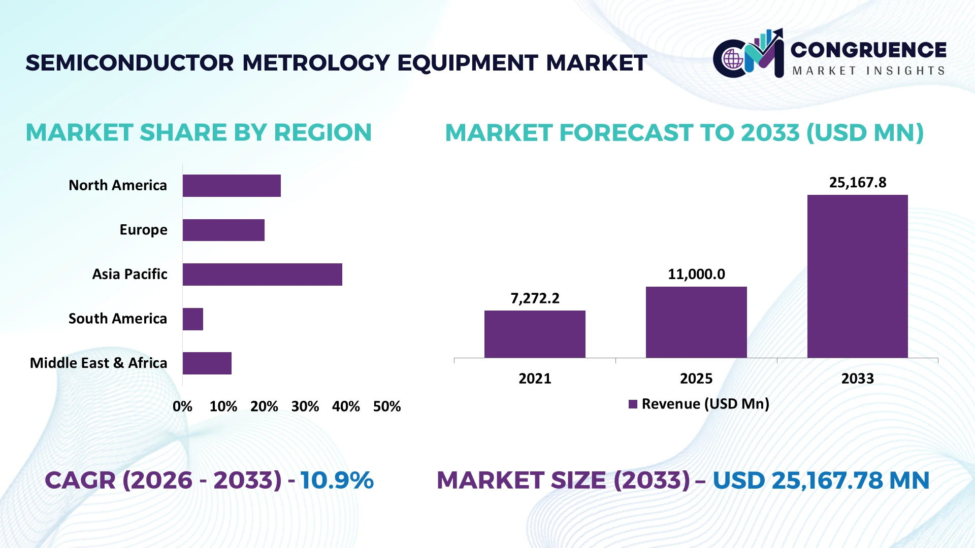
Taiwan leads semiconductor metrology deployment with an estimated 24% market share, supported by advanced foundries and high-volume wafer fabrication. South Korea follows at approximately 18%, driven by memory production and advanced-node investment. Taiwan's leading-edge fabs allocate substantial capital toward process-control infrastructure, while Japan's semiconductor equipment ecosystem remains stronger in materials and precision components. U.S.-China technology restrictions are accelerating localized semiconductor capacity investments and strengthening demand for advanced inspection and measurement capabilities.
Strategic priority is shifting toward high-precision metrology platforms that protect yield, process stability, and advanced-node investment returns.
Market Size & Growth: USD 11000 Million in 2025 to USD 25167.78 Million by 2033 at 10.9% CAGR, driven by advanced-node scaling.
Top Growth Drivers: Advanced packaging 32%, EUV adoption 29%, yield optimization 27%.
Short-Term Forecast: By 2028, automated metrology can reduce measurement cycles 25% and improve process efficiency 18%.
Emerging Technologies: AI metrology, hybrid optical-electron-beam inspection, and high-NA EUV process control gain 20–30% deployment momentum.
Regional Leaders: Asia-Pacific approaches USD 15 billion, North America USD 5 billion, Europe USD 3.5 billion by 2033.
End-User Trends: Advanced-node fabs show approximately 35% higher metrology intensity than mature-node facilities.
Pilot Example: 2026 advanced-packaging programs target 20% lower defect-related rework through automated wafer inspection.
Competitive Landscape: KLA leads near 35%, followed by Applied Materials, ASML, Hitachi High-Tech, and Onto Innovation.
Regulatory & ESG Impact: Localized semiconductor policies support 15%–20% capacity expansion while advanced metrology reduces wafer waste.
Investment & Funding: More than USD 100 billion in announced global semiconductor manufacturing investments strengthens equipment demand and regional supply-chain localization.
Innovation & Future Outlook: AI-driven analytics and multi-modal metrology will shift competition toward real-time yield intelligence through 2028.
The Semiconductor Metrology Equipment Market is increasingly concentrated around advanced logic, memory, and heterogeneous packaging facilities requiring nanometer-level process control. AI-enabled inspection, hybrid metrology, and automated defect classification are strengthening deployment, with advanced-node fabs recording roughly 35% higher metrology intensity than mature facilities. Geopolitical semiconductor capacity localization is also redirecting equipment investment toward regional manufacturing ecosystems, creating strategic opportunities for precision-tool suppliers and integrated process-control providers.
Semiconductor metrology equipment is becoming a strategic control point as chipmakers push advanced nodes, HBM, 3D integration, and heterogeneous packaging. Measurement accuracy increasingly determines whether expensive wafer capacity converts into usable yield. The industry is also restructuring supply chains around regional fabs, with Taiwan, South Korea, the United States, and India expanding semiconductor manufacturing infrastructure and strengthening localized equipment ecosystems.
AI-assisted metrology and in-line process control are replacing slower offline measurement workflows. Compared with conventional sampling-based inspection, automated data-driven systems can reduce measurement-cycle time by roughly 25% and improve process-response speed by about 20%. Taiwan remains the leading advanced-manufacturing hub, while South Korea is intensifying HBM and memory capacity; the United States is emphasizing domestic semiconductor resilience and technology localization.
From 2026 to 2028, metrology deployment will increasingly move toward real-time, multi-modal measurement integrated directly with fab execution systems. Advanced packaging is a practical example: wafer-level inspection now addresses bonded, thinned, warped, and diced substrates. Companies are therefore prioritizing AI-enabled platforms, application-specific partnerships, and local service capabilities. Competitive advantage will increasingly depend on measurement sensitivity, data integration, and the ability to protect yield during rapid process transitions.
Shrinking geometries and heterogeneous integration are increasing process-control intensity across leading semiconductor fabs. Advanced packaging programs are expanding metrology requirements by approximately 30%, while AI-assisted inspection can improve defect-classification productivity by nearly 25%. South Korea's aggressive HBM capacity expansion is reinforcing investment in wafer and package-level measurement systems. As process windows narrow, manufacturers cannot rely on periodic offline sampling alone. Equipment providers are responding with in-line optical metrology, e-beam inspection, AI analytics, and automated process feedback. The strategic shift is significant: metrology is moving from quality verification toward real-time yield management, allowing fabs to identify process excursions earlier and protect high-value wafer output.
High-end metrology systems require substantial capital, specialized installation, and tightly controlled fab environments, limiting rapid deployment outside advanced manufacturing clusters. Complex integration can increase implementation workloads by approximately 20%, while calibration and maintenance requirements can add 10%–15% to operating expenditure. China's semiconductor equipment ecosystem also faces restrictions on access to certain advanced technologies amid evolving export controls, complicating procurement and qualification strategies. These constraints can extend equipment qualification cycles and reduce utilization during early fab ramp-up. Manufacturers are responding through multi-year supplier agreements, regional service networks, equipment localization, and greater use of modular platforms. The operational priority is maximizing tool utilization rather than simply expanding installed capacity.
AI-enabled metrology creates an opportunity to connect measurement data directly with process-control systems, reducing manual engineering intervention and accelerating corrective action. Predictive analytics can improve anomaly-detection efficiency by approximately 25%, while virtual metrology approaches can reduce selected physical measurement workloads by around 15%. India is emerging as a new semiconductor manufacturing location, creating demand for localized process-control infrastructure alongside new fabrication and packaging capacity. Suppliers are investing in machine-learning models, digital twins, and multi-modal measurement platforms that combine optical and e-beam data. The less obvious opportunity is recurring software value: intelligent analytics can turn installed measurement hardware into continuously improving process-control infrastructure.
Three-dimensional architectures, chiplets, hybrid bonding, and buried interconnects are creating measurement challenges that conventional surface inspection cannot fully address. Industry research indicates that 54% of surveyed practitioners identify hybrid bonding as particularly difficult to analyze, while 83% support greater data standardization for advanced packaging workflows. Taiwan's high-volume packaging ecosystem faces increasing pressure to qualify complex structures without slowing production ramps. These requirements increase integration complexity across metrology, inspection, simulation, and manufacturing-execution systems. Equipment suppliers must therefore improve non-destructive measurement, cross-platform data interoperability, and automated defect classification. Long-term competitiveness will depend on delivering consistent measurement intelligence across front-end wafer fabrication and increasingly complex back-end packaging processes.
AI-Driven Measurement Analytics: AI-assisted defect classification is moving into production workflows, with automation improving analysis productivity by roughly 25% and reducing engineer review time by 15%. U.S. fabs are integrating machine-learning analytics with inspection data, while suppliers expand software capabilities to accelerate excursion response and reduce engineering bottlenecks.
Advanced Packaging Measurement Shift: 3D packaging and HBM are increasing measurement complexity, with advanced packaging equipment demand rising 21% in 2025 and test intensity accelerating. Taiwan and South Korea are expanding inspection capacity, while equipment companies develop multi-dimensional measurement solutions for warpage, bonding, and buried structures.
Localized Fab Equipment Ecosystems: Supply-chain restructuring is shifting equipment qualification closer to new manufacturing sites. China, Taiwan, and Korea represented 79% of global semiconductor equipment spending in 2025, prompting suppliers to strengthen local service, calibration, and application-engineering networks to protect installation speed and uptime.
Hybrid Metrology Integration: Hybrid optical, AFM, and spectroscopic techniques are increasingly combined to address complex 3D structures, with integrated workflows targeting 20% faster characterization and broader wafer coverage. Research-industry collaborations are expanding, while suppliers prioritize multi-modal platforms rather than standalone measurement tools.
Optical Metrology leads the Semiconductor Metrology Equipment Market with an estimated 48% share, supported by high throughput, non-destructive measurement, and compatibility with high-volume wafer fabrication. Its deployment advantage is strongest in critical dimension, overlay, film thickness, and defect monitoring, where automated optical systems support continuous process control. E-Beam Metrology follows with approximately 27% share and commands premium demand where nanometer-scale resolution is essential. Optical platforms deliver roughly 30% faster measurement throughput than many high-resolution electron-beam workflows, strengthening their economics in high-volume fabs.
E-Beam Metrology is the fastest-growing type, driven by sub-3nm structures and increasingly complex pattern verification, with adoption expanding approximately 18%. X-Ray Metrology retains importance for buried structures and advanced packaging, while Scatterometry supports rapid dimensional and profile characterization. Equipment manufacturers are prioritizing hybrid architectures, higher automation, and software integration, shifting investment toward platforms that combine throughput with nanoscale sensitivity rather than optimizing either metric independently.
Wafer Inspection accounts for approximately 42% of market demand, reflecting its broad deployment across front-end fabrication and its role in identifying defects before additional processing costs accumulate. Automated inspection improves detection workflow efficiency by nearly 28%, making it particularly valuable at high-volume fabs. Process Control follows closely at around 31%, where real-time measurement increasingly links equipment data with fab execution systems. The shift from periodic sampling toward continuous monitoring is strengthening demand for integrated metrology platforms.
Critical Dimension Measurement is the fastest-growing application, expanding approximately 19% as advanced nodes narrow process windows and require tighter dimensional control. Thin Film Measurement remains strategically important for deposition and multilayer structures, particularly in memory and advanced logic. Suppliers are integrating AI analytics, automated classification, and cross-tool data management, enabling manufacturers to reduce engineering response times while increasing measurement coverage without proportionally increasing labor requirements.
Semiconductor Foundries represent the leading end-user group with approximately 44% market share, driven by high wafer volumes, multi-customer process qualification, and aggressive technology-node transitions. Their metrology intensity is approximately 25% higher than that of many mature-node production environments because yield management must accommodate frequent process changes. Integrated Device Manufacturers account for roughly 34%, retaining strong demand through vertically integrated control of device design and fabrication.
OSAT Companies are the fastest-growing end-user segment, with adoption increasing approximately 20% as advanced packaging, chiplets, and HBM raise measurement requirements beyond conventional assembly inspection. Research Institutes remain smaller but strategically influential, supporting early-stage process development and equipment qualification. Vendors are responding with application-specific configurations, collaborative development programs, and flexible service models. The competitive priority is shifting toward platforms that serve both production-scale foundries and specialized packaging environments without sacrificing measurement precision or throughput.
Asia-Pacific accounted for the largest market share at 58% in 2025 however, Middle East & Africa is expected to register the fastest growth, expanding at a CAGR of 12.4% between 2026 and 2033.
Domestic Fab Expansion Reshapes Process-Control Deployment
North America holds a strong position in semiconductor metrology through advanced logic, memory, aerospace electronics, and domestic fabrication expansion. The United States accounts for the majority of regional demand, supported by new fabrication projects and modernization of established fabs. More than 32% of regional metrology deployments are concentrated around leading-edge wafer fabrication and advanced packaging environments. Federal semiconductor incentives are accelerating equipment localization, while suppliers are expanding application-engineering and service capabilities near major manufacturing clusters. AI-assisted inspection and automated process control are gaining traction as fabs seek tighter yield management. Equipment providers are increasing partnerships with chipmakers and expanding local technical support to reduce qualification delays and improve tool utilization.
United States Market Outlook: The United States remains the region's primary market because of its expanding advanced-node manufacturing base, strong equipment ecosystem, and concentration of semiconductor R&D. More than 25 major fabrication and packaging projects are progressing across the country, increasing demand for optical, e-beam, and X-ray measurement systems. Domestic manufacturing policies are also encouraging suppliers to strengthen localized service and integration capabilities.
Precision Engineering Meets Semiconductor Reshoring
Europe's semiconductor metrology demand is concentrated around Germany, France, the Netherlands, and Italy, where automotive electronics, power semiconductors, sensors, and equipment engineering support specialized measurement requirements. Approximately 21% of regional demand is associated with automotive and industrial semiconductor production. European chip initiatives are strengthening local fabrication capacity and equipment supply-chain resilience, while sustainability targets are encouraging fabs to improve wafer utilization and reduce process scrap. Germany's industrial automation base and the Netherlands' semiconductor equipment expertise support high-value metrology deployment. Suppliers are expanding application-specific solutions and collaborative development programs to address advanced packaging, compound semiconductors, and mature-node optimization.
Germany Market Outlook: Germany represents Europe's strongest industrial demand center, supported by automotive semiconductor production, power electronics, and precision manufacturing capabilities. Semiconductor investment projects are expanding fabrication infrastructure and increasing requirements for automated process monitoring. More than 20% of European semiconductor manufacturing capacity is linked to automotive applications, strengthening demand for high-accuracy metrology that supports reliability, yield, and stringent quality requirements.
Fab Concentration Creates Unmatched Equipment Scale
Asia-Pacific dominates the Semiconductor Metrology Equipment Market because Taiwan, South Korea, Japan, and China combine high-volume wafer fabrication, memory production, advanced packaging, and extensive semiconductor equipment ecosystems. The region represents approximately 58% of global market demand, with Taiwan and South Korea accounting for a substantial share of leading-edge deployments. Advanced-node and HBM production are increasing inspection intensity, while new fabrication projects are expanding installed measurement capacity. Suppliers are strengthening local service teams, application centers, and strategic partnerships to shorten qualification cycles. Taiwan's foundry ecosystem prioritizes high-throughput optical and e-beam metrology, while South Korea emphasizes memory and advanced packaging process control.
Taiwan Market Outlook: Taiwan remains the most strategically important country because of its concentration of advanced foundries and sophisticated semiconductor manufacturing infrastructure. Leading fabs increasingly deploy automated metrology across critical process steps, with advanced-node production requiring substantially tighter dimensional and overlay control than mature processes. Equipment suppliers are expanding local engineering support to maintain rapid qualification and high tool availability.
Emerging Electronics Capacity Builds Selective Demand
South America represents a smaller but strategically relevant market, with Brazil accounting for most regional semiconductor-related equipment activity through electronics manufacturing, research programs, and industrial technology initiatives. Approximately 14% of regional semiconductor equipment demand is associated with research, prototyping, and specialized electronics production rather than high-volume leading-edge fabrication. Brazil's domestic technology initiatives are supporting greater semiconductor capability, while limited advanced-fab infrastructure constrains demand for high-end e-beam and critical-dimension systems. Suppliers are responding through distributor partnerships, application support, and flexible equipment configurations. The strongest opportunity lies in specialized metrology for mature-node devices, compound materials, sensors, and advanced electronics rather than immediate high-volume logic manufacturing.
Brazil Market Outlook: Brazil is the region's leading market because of its larger electronics manufacturing base, research infrastructure, and government-supported semiconductor initiatives. Local semiconductor programs are increasing requirements for wafer characterization and process measurement. Research institutions and specialized manufacturers represent important buyers, creating demand for flexible metrology platforms that can support multiple device structures without requiring the infrastructure of a leading-edge fab.
Strategic Technology Investment Builds New Capacity
Middle East & Africa is developing a semiconductor technology ecosystem through diversification programs, advanced electronics investment, research infrastructure, and high-performance computing initiatives. Demand remains concentrated in the United Arab Emirates, Saudi Arabia, Israel, and selected African technology centers, with approximately 17% of regional semiconductor-related equipment activity linked to research, advanced electronics, and specialized manufacturing. Israel provides a strong technology base through semiconductor design and engineering capabilities, while Gulf economies are investing in digital infrastructure and industrial diversification. Equipment suppliers are forming local partnerships and expanding technical support to establish early-market positions before fabrication capacity scales further.
United Arab Emirates Market Outlook: The United Arab Emirates is emerging as a strategic technology hub through investment in advanced computing, electronics infrastructure, and semiconductor-related research. Its strong data-center ecosystem and technology investment environment support demand for precision characterization and inspection capabilities. Partnerships with international technology providers are strengthening local expertise and creating a foundation for broader semiconductor equipment deployment.
KLA, Applied Materials, ASML, Hitachi High-Tech, and Onto Innovation compete as technology leaders, while specialized metrology developers target niche applications and regional service providers compete on customization and cost. The top five players collectively command approximately 72% market share, creating a concentrated structure built around technology depth, installed-base strength, and application expertise. Competition centers on measurement accuracy, throughput, integration, and service responsiveness. Advanced platforms improve measurement productivity by 20%–30%, while automated data analysis can reduce engineering intervention by roughly 15%. Companies are expanding application centers, partnering with foundries, and integrating AI analytics to strengthen equipment differentiation. The competitive shift is moving toward hybrid metrology, where optical, e-beam, and computational capabilities operate within unified process-control workflows. High R&D requirements, qualification cycles, intellectual property, and fab integration create substantial entry barriers. Winning requires superior measurement performance, rapid qualification, dependable global service, and deep integration with customer process-control architectures.
KLA Corporation
Applied Materials, Inc.
ASML Holding N.V.
Hitachi High-Tech Corporation
Onto Innovation Inc.
Nova Ltd.
Thermo Fisher Scientific Inc.
Bruker Corporation
JEOL Ltd.
Rigaku Corporation
SCREEN Semiconductor Solutions Co., Ltd.
Lasertec Corporation
Camtek Ltd.
Rudolph Technologies
Current semiconductor metrology is shifting toward AI-assisted optical, e-beam, and hybrid measurement systems integrated with automated process-control platforms. Hitachi High-Tech’s GT2000 delivers 25% higher throughput than previous models while reducing lifecycle CO₂ emissions by 50%. KLA and Onto Innovation are embedding AI-guided analytics, enabling fabs to connect measurement, defect classification, and yield decisions within production workflows.
Emerging technologies include high-resolution e-beam metrology for GAA structures, optical critical-dimension measurement for HBM, and 3D metrology for advanced packaging. Applied Materials introduced PROVision 10 in 2025 with sub-nanometer resolution for complex 3D chips, while Onto Innovation’s Atlas G6 targets geometries shrinking up to 30% per generation. These platforms strengthen measurement precision while reducing process excursions and engineering intervention.
From 2026–2028, computational metrology, virtual measurement, multimodal data fusion, and AI-based process prediction will become increasingly important as fabs integrate metrology with manufacturing-execution and advanced process-control systems. New platforms outperform legacy workflows through faster measurement and richer analytics, giving advanced-node foundries and HBM manufacturers the strongest competitive advantage. Acting now secures tool qualification, data integration, and yield-learning benefits before process complexity increases further.
October 2025 Applied Materials introduced PROVision 10 eBeam metrology for complex 3D chips, delivering sub-nanometer resolution and fast throughput. The platform targets GAA, HBM, and advanced packaging, strengthening yield control for AI semiconductor production. Source: Applied Materials
September 2025 Onto Innovation launched Atlas G6 optical OCD metrology for GAA and HBM, addressing structures shrinking up to 30% per generation. The system strengthens dimensional control as advanced AI devices demand tighter process windows. Source: Onto Innovation
September 2025 Hitachi High-Tech highlighted GT2000 CD-SEM improvements delivering 25% higher processing capability and 50% lower lifecycle CO₂ emissions versus its FY2010 standard. The development combines higher productivity with measurable sustainability benefits. Source: Hitachi High-Tech
April 2026 SEMI reported global semiconductor equipment sales reached $135.1 billion in 2025, increasing 15% year over year. Taiwan, Korea, and China represented 79% of spending, reinforcing Asia's concentration of advanced manufacturing investment and metrology demand. Source: SEMI
The Semiconductor Metrology Equipment Market report covers Optical Metrology, E-Beam Metrology, X-Ray Metrology, and Scatterometry across Wafer Inspection, Process Control, Thin Film Measurement, and Critical Dimension Measurement. End-user analysis includes Semiconductor Foundries, Integrated Device Manufacturers, OSAT Companies, and Research Institutes, providing visibility across production-scale and specialized measurement environments.
The study evaluates North America, Europe, Asia-Pacific, South America, and Middle East & Africa, with focused analysis of advanced-node fabrication, HBM, GAA, 3D packaging, and AI-enabled metrology. It assesses technology adoption, deployment intensity, competitive positioning, supplier strategies, and emerging measurement architectures through 2026–2033. The resulting framework supports equipment investment prioritization, geographic expansion, partnership decisions, product development, and competitive positioning as fabs transition toward increasingly automated and data-driven process control.
| Report Attribute/Metric | Report Details |
|---|---|
Market Revenue in 2025 | USD 11000 Million |
Market Revenue in 2033 | USD 25167.78 Million |
CAGR (2026 - 2033) | 10.9% |
Base Year | 2025 |
Forecast Period | 2026 - 2033 |
Historic Period | 2021 - 2025 |
Segments Covered | By Type
By Application
By End-User
|
Key Report Deliverable | Revenue Forecast, Growth Trends, Market Dynamics, Segmental Overview, Regional and Country-wise Analysis, Competition Landscape |
Region Covered | North America, Europe, Asia-Pacific, South America, Middle East, Africa |
Key Players Analyzed | KLA Corporation, Applied Materials, Inc., ASML Holding N.V., Hitachi High-Tech Corporation, Onto Innovation Inc., Nova Ltd., Thermo Fisher Scientific Inc., Bruker Corporation, JEOL Ltd., Rigaku Corporation, SCREEN Semiconductor Solutions Co., Ltd., Lasertec Corporation, Camtek Ltd., Rudolph Technologies |
Customization & Pricing | Available on Request (10% Customization is Free) |