
Reports
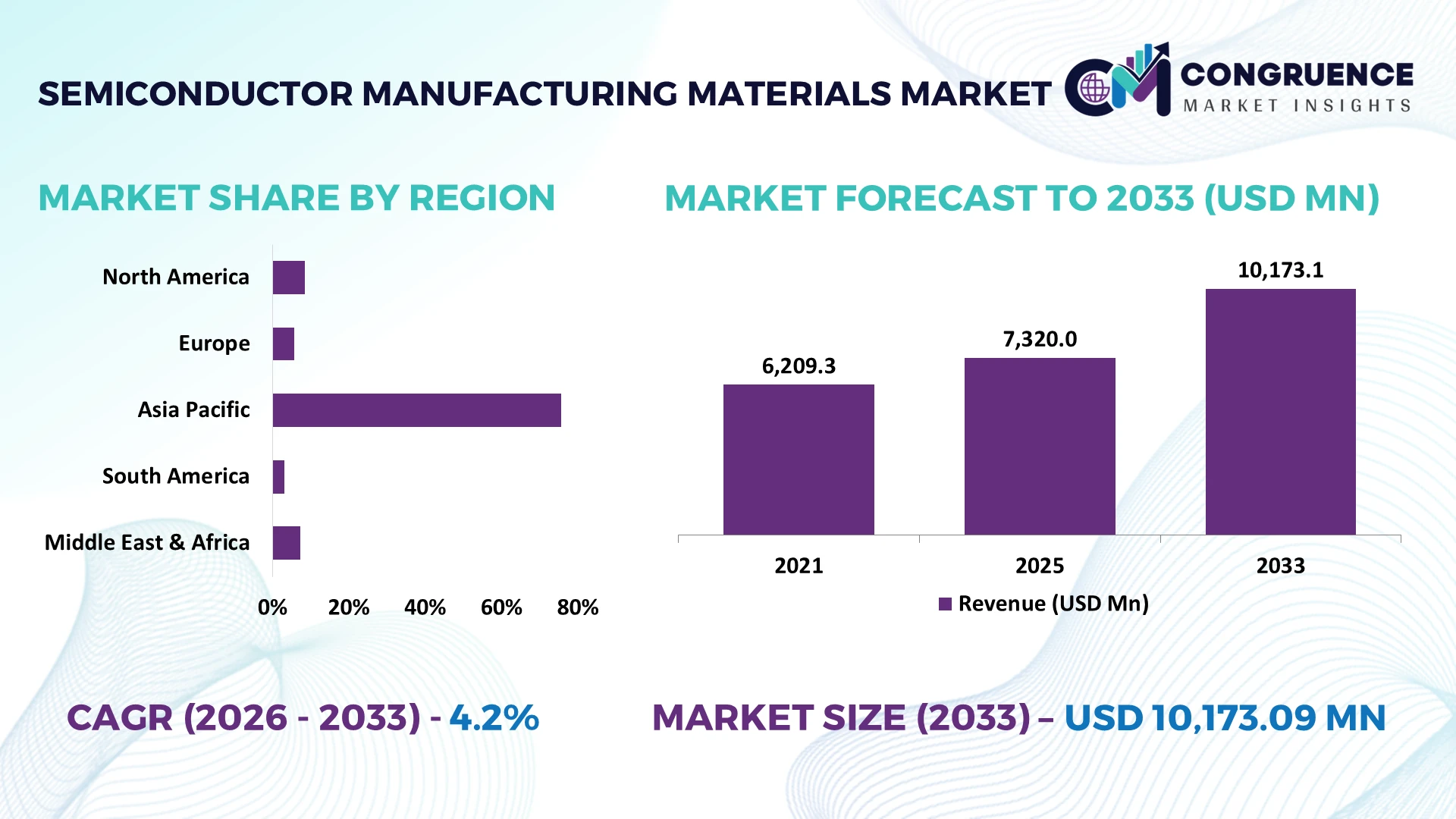
The Global Semiconductor Manufacturing Materials Market was valued at USD 7,320.0 Million in 2025 and is anticipated to reach a value of USD 10,173.1 Million by 2033 expanding at a CAGR of 4.2% between 2026 and 2033. Growth is driven by increasing consumption of EUV photoresists, high-purity process chemicals, specialty gases, advanced silicon wafers, and next-generation packaging substrates as AI accelerators and high-bandwidth memory intensify fabrication requirements.
Taiwan dominates semiconductor materials consumption, accounting for approximately 29.6% of the broader global materials market in 2025, supported by TSMC's advanced fabrication ecosystem and extensive supplier networks. China follows with approximately 21.3%, driven by domestic semiconductor localization and fabrication capacity expansion. Taiwan's concentration of advanced-node manufacturing reinforces its strategic importance, while US-China technology restrictions accelerate supply-chain diversification and regional materials qualification.
Strategically, suppliers must prioritize localized production, advanced-material innovation, and long-term agreements with leading foundries to secure access to high-value fabrication programs.
Market Size & Growth: USD 7,320.0 million in 2025, reaching USD 10,173.1 million by 2033, supported by advanced-node fabrication and AI semiconductor production.
Top Growth Drivers: Advanced packaging materials increased 9.3%, wafer fabrication materials 5.4%, and China's materials consumption 12.5% in 2025.
Short-Term Forecast: By 2028, increasing process automation and chemical recycling adoption will strengthen manufacturing consistency and resource efficiency.
Emerging Technologies: EUV photoresists, atomic-layer deposition precursors, high-purity specialty gases, and advanced packaging substrates are reshaping materials specifications.
Regional Leaders: Taiwan recorded USD 21.7 billion, China USD 15.6 billion, and South Korea USD 11.2 billion in 2025 materials consumption, reflecting concentrated foundry, memory, and domestic fabrication activity.
Consumer/End-User Trends: Advanced logic, HBM, and 3D NAND manufacturers increasingly prioritize contamination-controlled materials and application-specific chemical formulations.
Pilot/Case Example: TSMC's 2024 sustainability program strengthened supplier engagement through 63 water-management sessions involving 1,930 participants.
Competitive Landscape: The fabrication-materials market remains fragmented, with Merck, Shin-Etsu Chemical, JSR, DuPont, and Cabot competing across specialty chemicals and wafer-processing materials.
Regulatory & ESG Impact: Semiconductor fabs recycle approximately 40–70% of received water under conventional onsite treatment, encouraging investment in closed-loop purification.
Investment & Funding: US CHIPS incentives, Japanese manufacturing initiatives, and Asian fabrication expansions are encouraging localized specialty-material production and supplier partnerships.
Innovation & Future Outlook: Next-generation photoresists, advanced deposition precursors, low-defect wafers, and recyclable processing chemicals will shift competition toward material purity and process-specific performance.
Semiconductor manufacturing materials encompass silicon wafers, photoresists, photomasks, specialty gases, wet chemicals, CMP slurries, deposition precursors, and advanced packaging materials. Demand is increasingly concentrated in EUV lithography, high-bandwidth memory, 3D NAND, and advanced logic fabrication. Packaging materials expanded 9.3% in 2025, outpacing wafer fabrication materials at 5.4%. Supplier qualification, chemical purity, and regional sourcing diversification are becoming essential procurement priorities as geopolitical restrictions reshape semiconductor supply chains.
Semiconductor manufacturing materials are becoming strategic assets because material purity, process compatibility, and supply reliability directly determine chip performance, production yields, and national technology competitiveness. The expansion of AI infrastructure, high-performance computing, and advanced memory manufacturing is shifting procurement toward specialized materials rather than conventional commodity inputs. US-China technology restrictions and semiconductor localization incentives are accelerating regional supplier diversification and domestic manufacturing investments.
The industry is also transitioning toward more complex material requirements. EUV-compatible photoresists and advanced deposition precursors support increasingly intricate transistor architectures, while advanced packaging materials recorded 9.3% growth in 2025 compared with 5.4% for wafer fabrication materials. Compared with conventional packaging, high-density interconnect and advanced substrate technologies enable more sophisticated chip integration and improved bandwidth utilization. Taiwan leads in manufacturing scale, while China emphasizes domestic sourcing and the United States strengthens its advanced fabrication ecosystem.
Over the next 2–3 years, suppliers will prioritize qualification at new fabrication facilities, automated chemical handling, contamination monitoring, and localized production. For example, TSMC's Arizona expansion is encouraging materials suppliers to establish closer relationships with US fabrication operations. Companies are increasing technical partnerships, regional distribution capabilities, and application-specific R&D. Competitive advantage will increasingly depend on delivering consistent material quality, securing geographically diversified supply, and supporting next-generation manufacturing processes.
Increasing transistor complexity and EUV lithography adoption are intensifying demand for high-purity photoresists, deposition precursors, specialty gases, and CMP slurries. In 2025, wafer fabrication materials expanded 5.4%, while lithography-related materials and wet chemicals recorded double-digit growth. Advanced DRAM, 3D NAND, and leading-edge logic require tighter contamination controls and additional precision-processing steps. Taiwan's advanced foundry ecosystem and South Korea's HBM investments are strengthening specialized material procurement. Japan-based chemical manufacturers and international suppliers are expanding application laboratories, production capabilities, and customer qualification programs. The non-obvious advantage lies in process-specific formulations: suppliers that reduce defectivity and improve material consistency gain stronger customer retention than commodity-focused competitors.
Manufacturing semiconductor-grade chemicals and gases requires stringent purification, contamination control, and specialized transportation infrastructure. Conventional semiconductor facilities recycle approximately 40–70% of received water, while ultra-pure water production requires substantial additional treatment. Producing 1,000 gallons of ultra-pure water requires approximately 1,400–1,600 gallons of municipal water. These requirements increase operating expenditure and expose suppliers to water availability, energy pricing, and chemical disposal constraints. Taiwan and Japan face particular pressure to maintain reliable industrial utilities around concentrated fabrication clusters. Companies are responding through closed-loop water systems, localized purification facilities, long-term utility agreements, and diversified chemical sourcing. The key restraint is not simply raw-material pricing but the cost of maintaining consistent semiconductor-grade purity at scale.
Advanced packaging creates attractive opportunities for specialized substrates, bonding materials, underfill formulations, photoresists, and thermal-management chemicals. Packaging materials expanded 9.3% in 2025, outperforming wafer fabrication materials and highlighting the increasing importance of heterogeneous integration and HBM production. Japanese and Taiwanese suppliers are positioned to benefit from advanced substrate development, while US fabrication investments create opportunities for localized specialty-material production. Semiconductor suppliers are expanding R&D in low-defect dielectric materials, high-performance bonding compounds, and next-generation deposition precursors. Another opportunity lies in reclaiming high-value process chemicals and developing formulations that reduce material consumption without compromising yield. Companies that establish early qualification partnerships with advanced packaging manufacturers can secure recurring demand before competing formulations become standardized.
Next-generation semiconductor production introduces increasingly demanding material compatibility, metrology, and contamination-control requirements. Advanced-node fabrication depends on tightly controlled chemical compositions, while HBM and 3D packaging introduce additional thermal, mechanical, and interfacial performance constraints. Semiconductor manufacturing water consumption increased 24.5% between 2019 and 2023, intensifying pressure on fabrication ecosystems to improve resource efficiency. Meanwhile, the concentration of specialized suppliers in Japan, Taiwan, South Korea, and China creates qualification and geopolitical exposure for international manufacturers. Companies must address these challenges through multi-source qualification, advanced analytical laboratories, cybersecurity protection for connected chemical-delivery systems, and workforce development. The strategic challenge is maintaining identical material performance across geographically distributed production facilities without increasing defect rates or environmental burdens.
Advanced Lithography Materials Gain Traction: EUV-compatible photoresists, photomasks, and photoresist ancillaries are experiencing stronger procurement as manufacturers transition toward sub-3nm fabrication. Lithography-related materials recorded double-digit growth in 2025, while silicon wafer shipments increased 5.8% to 12,973 million square inches. Japanese suppliers are strengthening specialty chemical development and customer qualification to address tighter patterning tolerances and reduce process defects.
Packaging Material Demand Accelerates: Packaging materials expanded 9.3% in 2025, compared with 5.4% for wafer fabrication materials, reflecting stronger demand for advanced substrates and high-bandwidth memory integration. Substrate manufacturers are increasing production capabilities, while bonding-wire suppliers are adjusting procurement strategies to manage gold-price volatility. This shift is strengthening investment in heterogeneous integration and high-density interconnect technologies, where material compatibility directly influences packaging yield.
Regional Sourcing Strategies Reshape: China recorded 12.5% growth in semiconductor materials consumption, while North America expanded 10.7% in 2025. US semiconductor localization incentives and export-control restrictions are encouraging suppliers to diversify production, qualify alternative sources, and establish regional distribution facilities. The non-obvious shift is that local technical qualification is becoming as important as manufacturing capacity, because new fabs require materials to pass extensive process-validation cycles before commercial deployment.
Silicon Wafer Specifications Become Stricter: Worldwide silicon wafer shipments increased 5.8% in 2025, supported by advanced logic and HBM applications, while wafer revenue declined 1.2%. This divergence reflects changing product mix and pricing pressure rather than uniform demand recovery. Manufacturers are prioritizing 300mm polished and epitaxial wafers, improving surface quality, and aligning production with sub-3nm requirements. Suppliers are consequently emphasizing yield consistency, specialized wafer engineering, and long-term foundry qualification instead of volume-led expansion.
Wafer fabrication materials dominated the global semiconductor manufacturing materials market, accounting for approximately 62.6% of total market value in 2025. Silicon wafers, photomasks, photoresists, electronic specialty gases, wet chemicals, and CMP consumables sustain this position through their essential role in front-end chip production. Silicon wafers represent the largest individual material category, supported by widespread 300mm wafer adoption and compatibility with advanced logic, memory, and power semiconductor manufacturing. Packaging materials accounted for approximately 37.4%, but demonstrated stronger growth as advanced substrates, bonding wire, and die-attach materials gained importance in high-bandwidth memory and heterogeneous integration.
Packaging materials represent the faster-expanding category, increasing 9.3% in 2025 compared with 5.4% for wafer fabrication materials. Photoresists, wet chemicals, and other lithography-related materials also recorded double-digit growth. Manufacturers are strengthening specialty formulations, substrate production, and application-specific qualification capabilities. Investment priorities are shifting toward advanced packaging without reducing the strategic importance of established wafer-processing materials.
Logic and foundry manufacturing represents the leading application for semiconductor manufacturing materials, accounting for an estimated 50.0% of application-related material consumption in 2025. Advanced processors, GPUs, application-specific integrated circuits, and high-performance computing devices require extensive lithography, deposition, etching, and planarization processes. Memory manufacturing represents another major application, supported by DRAM, NAND, and high-bandwidth memory production. Power semiconductors, discrete devices, analog components, and sensors account for additional demand through specialized wafer substrates, electronic chemicals, and deposition materials. The increasing complexity of advanced logic manufacturing sustains higher material requirements per wafer compared with several mature semiconductor applications.
Memory manufacturing represents an increasingly important growth area as AI infrastructure expands HBM and advanced DRAM production. Logic and foundry applications retain scale advantages, while memory producers intensify investments in deposition chemicals, specialty gases, and precision polishing materials. Manufacturers are adapting formulations to improve defect control and process consistency. Suppliers are prioritizing application-specific partnerships with foundries and memory producers to strengthen long-term procurement relationships.
Integrated device manufacturers (IDMs) and pure-play foundries represent the largest collective end-user purchasing groups because they operate extensive wafer fabrication facilities and procure materials across multiple manufacturing stages. IDMs integrate semiconductor design and production, creating recurring requirements for silicon wafers, photoresists, specialty gases, wet chemicals, and CMP consumables. Pure-play foundries, particularly those operating advanced-node facilities, require highly consistent material specifications and extensive supplier qualification. Memory manufacturers represent another important purchasing category, with procurement concentrated around DRAM, NAND, and HBM fabrication. OSAT providers primarily consume packaging substrates, bonding wire, mold compounds, encapsulants, and die-attach materials.
Memory manufacturers and OSAT providers represent important growth-oriented customer groups as AI computing increases demand for advanced memory integration and sophisticated packaging. Power and compound semiconductor manufacturers also strengthen demand for SiC, GaN, and other specialized substrate materials. Unlike large foundries, these specialized manufacturers prioritize application-specific formulations and long-term technical support. Suppliers are responding through dedicated account management, localized technical laboratories, customized material development, and strategic supply agreements. Competitive positioning increasingly depends on qualification speed and the ability to support multiple fabrication and packaging technologies.
Asia-Pacific accounted for the largest market share at 75.5% in 2025 however, North America is expected to register the fastest growth, expanding at a CAGR of 10.7% between 2026 and 2033.
North America accounted for approximately 8.5% of global semiconductor materials consumption in 2025. The United States dominates regional activity through advanced logic fabrication, memory production, specialty semiconductor manufacturing, and expanding packaging infrastructure. Regional materials consumption increased 10.7% during 2025, reflecting stronger fabrication activity and supplier localization. Arizona, Texas, and New York are important investment destinations, attracting wafer suppliers, specialty gas manufacturers, chemical processors, and equipment ecosystem partners. The US CHIPS and Science Act continues to encourage domestic production capacity and resilient procurement networks. Suppliers are establishing technical support facilities closer to fabrication clusters to reduce qualification delays and transportation exposure. The strategic shift is toward geographically secure, application-specific material supply rather than dependence on overseas sourcing alone.
United States Market Outlook: The United States leads North American semiconductor materials demand through its concentration of advanced fabrication projects, technology developers, and research institutions. Federal semiconductor incentives support domestic manufacturing expansion, while Arizona's TSMC facilities and Intel's manufacturing investments strengthen demand for high-purity chemicals, silicon wafers, specialty gases, and advanced packaging inputs. The US semiconductor industry also benefits from established materials research and engineering capabilities, allowing suppliers to accelerate customer qualification and develop specialized formulations.
Europe represented approximately 5.7% of global semiconductor materials consumption in 2025. Germany, France, Ireland, and the Netherlands anchor regional activity through automotive electronics, industrial automation, power semiconductors, and advanced lithography technologies. However, regional materials consumption declined 6.0% in 2025, reflecting weaker manufacturing demand and uneven semiconductor investment. The European Chips Act targets mobilization of more than EUR 43 billion in policy-supported investment to strengthen regional semiconductor capabilities. Automotive electrification and industrial power conversion continue to support demand for silicon carbide substrates, specialty gases, deposition chemicals, and wafer-processing consumables. Suppliers are prioritizing collaboration with automotive semiconductor manufacturers and localized technical distribution. Europe's competitive advantage increasingly rests on specialized industrial materials and process technologies rather than manufacturing volume.
Germany Market Outlook: Germany is Europe's most strategically significant semiconductor manufacturing center, supported by Dresden's fabrication ecosystem and strong automotive and industrial electronics industries. Its semiconductor industry generated more than EUR 17 billion in revenue in 2025, while more than one-third of European chip production takes place in the country. Investments involving Infineon, GlobalFoundries, and other manufacturing participants strengthen demand for silicon wafers, specialty chemicals, photoresists, and power semiconductor materials.
Asia-Pacific dominated the global semiconductor manufacturing materials market with approximately 75.5% share in 2025. Taiwan, China, South Korea, and Japan collectively account for the region's substantial consumption through advanced logic, memory, foundry, and packaging operations. Taiwan alone generated USD 21.7 billion in materials consumption, followed by China at USD 15.6 billion and South Korea at USD 11.2 billion. China's materials consumption increased 12.5%, while Taiwan recorded 8.6% growth. The concentration of advanced fabrication facilities supports strong procurement of silicon wafers, EUV photoresists, wet chemicals, specialty gases, and packaging substrates. Regional manufacturers are strengthening domestic sourcing, supplier qualification, and production partnerships. Export controls and geopolitical tensions are accelerating diversification, but the region's integrated manufacturing ecosystem continues to provide significant cost, scale, and technical advantages.
Taiwan Market Outlook: Taiwan maintains the strongest individual country position in semiconductor materials consumption through TSMC's advanced foundry ecosystem and the supporting operations of UMC and specialized packaging manufacturers. Its leading-edge fabrication capabilities sustain high demand for EUV photoresists, advanced silicon wafers, CMP slurries, specialty gases, and ultra-pure chemicals. The country's dense supplier network also enables rapid technical qualification and close collaboration between materials developers and semiconductor manufacturers, reinforcing its importance in global advanced-chip production.
South America represented an estimated 3.1% of the global market in the regional allocation, with Brazil accounting for the largest share of regional semiconductor-related activity. The market is supported by automotive electronics, telecommunications equipment, industrial automation, consumer electronics, and renewable energy systems. Regional manufacturing remains more concentrated in semiconductor assembly, testing, and electronic component integration than advanced wafer fabrication. Brazil's semiconductor policy initiatives and the expansion of local electronics manufacturing are encouraging demand for packaging compounds, specialty chemicals, substrates, and imported silicon wafers. However, limited advanced fabrication infrastructure and dependence on imported high-purity materials constrain local supplier development. Companies are focusing on distribution partnerships, technical service networks, and localized packaging capabilities. The strongest commercial opportunity lies in supporting regional electronics production rather than immediately replicating advanced Asian fabrication ecosystems.
Brazil Market Outlook: Brazil leads South America's semiconductor ecosystem through its electronics manufacturing base, automotive industry, telecommunications infrastructure, and government-backed semiconductor development initiatives. The country's PADIS industrial policy supports semiconductor and display manufacturing through fiscal incentives, strengthening investment conditions for domestic industry participants. Demand is concentrated in discrete devices, power electronics, sensors, and assembly-related materials. Suppliers benefit from partnerships with local electronics manufacturers and research institutions, particularly where imported materials require localized technical support and qualification.
Middle East & Africa accounted for an estimated 7.2% share in the indicative regional allocation, although this figure includes an unallocated portion of SEMI's Rest of World category and should not be interpreted as a verified continental market share. Semiconductor materials demand is emerging through telecommunications infrastructure, data centers, industrial automation, defense electronics, and renewable energy investments. The United Arab Emirates, Saudi Arabia, Israel, and South Africa represent important technology and electronics development centers. Government-backed diversification strategies and digital infrastructure investments are encouraging interest in semiconductor assembly, specialty material distribution, and localized manufacturing partnerships. However, limited advanced wafer fabrication capacity and dependence on imported specialty chemicals constrain immediate market expansion. Suppliers are prioritizing distribution agreements, technical partnerships, and investment feasibility assessments rather than large-scale standalone production facilities.
Israel Market Outlook: Israel represents a strategically important semiconductor technology center through its established chip design, research, and manufacturing ecosystem. Intel's operations in Kiryat Gat and the country's semiconductor innovation network support demand for high-purity chemicals, specialty gases, silicon wafers, and advanced fabrication inputs. Its concentration of semiconductor engineering expertise and international technology partnerships creates opportunities for specialized materials suppliers. Continued investment in fabrication infrastructure and process innovation strengthens Israel's position as an important technology-oriented market within the broader Middle East and Africa landscape.
Merck KGaA, Shin-Etsu Chemical, JSR, DuPont, and Cabot compete with specialty-gas suppliers Linde and Air Liquide, wafer leaders SUMCO and GlobalWafers, and packaging-material specialists. Competition is category-specific: Japanese firms lead photoresists and silicon wafers, while US and European groups contest purification, CMP, and process chemicals. The top five suppliers hold a combined 14.96% of the semiconductor fabrication-material subset in a 2025 estimate; this is not a verified share for the broader wafer-fab-plus-packaging market. Fragmentation leaves room for challengers. Price matters, but purity, defect control, qualification speed, and continuity dominate advanced-node awards; packaging materials grew 9.3% in 2025 versus 5.4% for wafer-fab materials. Players are expanding local plants, co-developing formulations with foundries, and securing long-term supply contracts. Export controls and customer localization are shifting competition toward regional capacity. Long qualification cycles and ultra-pure process requirements deter entrants. Winning requires proven yield, reliable local supply, and rapid co-innovation.
Merck KGaA
Shin-Etsu Chemical Co., Ltd.
JSR Corporation
DuPont de Nemours, Inc.
Entegris, Inc.
Air Liquide S.A.
Linde plc
SUMCO Corporation
GlobalWafers Co., Ltd.
Siltronic AG
SK Siltron Co., Ltd.
Tokyo Ohka Kogyo Co., Ltd.
BASF SE
Sumitomo Chemical Co., Ltd.
Semiconductor materials technology is shifting from commodity-grade inputs toward formulations for EUV patterning, sub-3nm logic, HBM, and 3D integration. Metal-oxide resists and next-generation chemically amplified photoresists improve pattern fidelity, while atomic-layer deposition precursors enable conformal films across high-aspect-ratio structures. JSR’s 2025 collaboration with Lam Research on dry resist, atomic-layer etching, and deposition materials illustrates how suppliers are co-developing inputs with equipment makers.
Advanced packaging is the second disruptive frontier. Substrates, low-warpage dielectric materials, thermal interface compounds, and fine-pitch bonding materials support chiplets and HBM stacks. Packaging materials grew 9.3% in 2025, faster than wafer-fab materials at 5.4%, signaling a stronger materials mix shift. Compared with conventional 200mm wafers, 300mm wafers provide 2.25 times the surface area per wafer, supporting higher production capacity. Suppliers with substrate and CMP expertise benefit most.
Automation and digital quality systems are becoming essential for chemical delivery, filtration, and contamination monitoring. With 300mm wafers representing roughly 80% of shipped wafer area, defect reductions directly protect yield. During 2026–2028, fabs will accelerate closed-loop chemical monitoring, AI-assisted defect analytics, and co-qualified materials ecosystems. Suppliers should invest now in application labs, regional support, and validated low-contamination formulations to secure design-in positions.
April 2024 — Shin-Etsu Chemical selected a 150,000 m² site in Isesaki, Japan, for its fourth semiconductor lithography-materials base, committing approximately ¥83 billion through phase one by 2026. The expansion adds R&D and production resilience for advanced nodes. Source: shinetsu.co.jp
August 2025 — Entegris announced a further $700 million US R&D and capital investment, bringing planned domestic investment to $1.4 billion. Its Aurora, Illinois technology center targets deposition materials, slurries, cleans, and CMP pads, supporting US supply-chain localization. Source: entegris.com
September 2025 — JSR/Inpria and Lam Research signed a non-exclusive cross-licensing and collaboration agreement covering EUV dry resist, atomic-layer etching, and deposition materials. The partnership aligns materials chemistry with equipment processes for leading-edge patterning and manufacturing qualification scale. Source: jsr.co.jp
July 2025 — Air Liquide committed more than €250 million to three air-separation units, two hydrogen units, and related infrastructure in Dresden. The long-term contract secures high-purity gases for a major semiconductor customer, supporting supply-chain resilience locally. Source: airliquide.com
The report evaluates the global semiconductor manufacturing materials industry across wafer fabrication and packaging inputs, covering silicon and SOI wafers, photomasks, photoresists and ancillaries, specialty gases, wet chemicals, sputtering targets, CMP materials, substrates, leadframes, bonding wire, die-attach materials, mold compounds, encapsulants, and ceramic packages. Application coverage examines lithography, deposition, etching, cleaning, planarization, doping, assembly, flip-chip, wafer-level, and 2.5D/3D packaging. End-user analysis includes IDMs, pure-play foundries, memory producers, OSAT providers, and power and compound-semiconductor manufacturers.
Regional coverage spans North America, Europe, Asia-Pacific, South America, and Middle East & Africa, with country-level focus on fabrication clusters and supplier ecosystems. Technology assessment tracks EUV materials, advanced precursors, HBM substrates, contamination control, and chemical recycling. The analysis supports supplier benchmarking, investment screening, localization decisions, expansion planning, and competitive positioning through 2033.
| Report Attribute / Metric | Details |
|---|---|
| Market Revenue (2025) | USD 7,320.0 Million |
| Market Revenue (2033) | USD 10,173.1 Million |
| CAGR (2026–2033) | 4.2% |
| Base Year | 2025 |
| Forecast Period | 2026–2033 |
| Historic Period | 2021–2025 |
| Segments Covered |
By Type
By Application
By End-User
|
| Key Report Deliverables | Revenue Forecast; Market Trends; Growth Drivers & Restraints; Technology Insights; Segmentation Analysis; Regional Insights; Competitive Landscape; Regulatory & ESG Overview; Recent Developments |
| Regions Covered | North America; Europe; Asia-Pacific; South America; Middle East & Africa |
| Key Players Analyzed | Merck KGaA; Shin-Etsu Chemical Co., Ltd.; JSR Corporation; DuPont de Nemours, Inc.; Entegris, Inc.; Air Liquide S.A.; Linde plc; SUMCO Corporation; GlobalWafers Co., Ltd.; Siltronic AG; SK Siltron Co., Ltd.; Tokyo Ohka Kogyo Co., Ltd.; BASF SE; Sumitomo Chemical Co., Ltd. |
| Customization & Pricing | Available on Request (10% Customization Free) |