
Reports
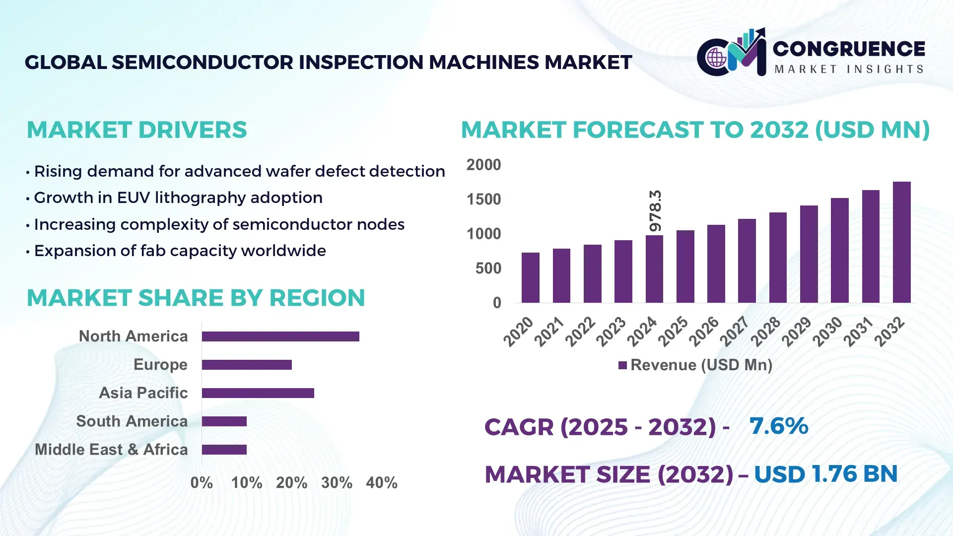
The Global Semiconductor Inspection Machines Market was valued at USD 978.32 Million in 2024 and is anticipated to reach a value of USD 1757.84 Million by 2032 expanding at a CAGR of 7.6% between 2025 and 2032. This growth is supported by rapid advances in wafer fabrication technologies and increased adoption of high-precision metrology systems.
The United States maintains a strong position in the Semiconductor Inspection Machines market due to its extensive fabrication ecosystem, high-volume capital expenditure, and sustained investment in advanced process control equipment. Multiple U.S.-based facilities operate inspection capacities exceeding 300,000 wafer starts per month supported by over USD 50 Billion in federal and private semiconductor investment programs since 2022. The country’s deployment of advanced EUV inspection tools, steady integration of AI-driven defect analytics, and accelerated expansion of 5 nm and below technology nodes further reinforce its leadership across multiple application segments.
• Market Size & Growth: Valued at USD 978.32 Million in 2024, projected to reach USD 1757.84 Million by 2032 at a CAGR of 7.6%, driven by rising defect-detection requirements in advanced semiconductor nodes.
• Top Growth Drivers: 42% increase in advanced node adoption, 38% improvement in inspection accuracy, 35% rise in AI-enabled process automation.
• Short-Term Forecast: By 2028, inspection cycle times are expected to improve by 28% through next-generation optical and e-beam systems.
• Emerging Technologies: Growth accelerated by EUV-compatible inspection systems, AI-powered metrology analytics, and hybrid optical–electron platforms.
• Regional Leaders: North America expected to reach USD 610 Million by 2032 with strong AI adoption; East Asia projected at USD 540 Million driven by high-volume fabs; Europe projected at USD 305 Million backed by automotive semiconductor demand.
• Consumer/End-User Trends: Increased uptake from logic, memory, and foundry operators emphasizing tighter process-control loops and higher yield assurance.
• Pilot or Case Example: A 2027 advanced-node pilot demonstrated a 32% reduction in defect-related downtime through integrated optical–e-beam inspection.
• Competitive Landscape: Market led by KLA Corporation with around 45% share, followed by Hitachi High-Tech, Applied Materials, Lasertec, and Onto Innovation.
• Regulatory & ESG Impact: Incentives for domestic chip manufacturing and energy-efficient fab tools are accelerating adoption of optimized inspection platforms.
• Investment & Funding Patterns: Over USD 20 Billion in recent semiconductor equipment investments focusing on process-control automation and next-generation inspection tools.
• Innovation & Future Outlook: Integration of AI-driven defect classification, intelligent metrology software, and EUV-compatible inspection tools shaping future production environments.
The Semiconductor Inspection Machines Market continues to evolve with rising demand from logic, memory, and advanced foundry operations, where defect-detection precision significantly influences output quality and cost efficiency. Recent advancements in multi-beam e-beam systems, AI-guided inspection algorithms, and EUV-layer metrology are reshaping production benchmarks across leading fabs. Regulatory support for semiconductor capacity expansion, regional scaling of 300 mm and emerging 450 mm wafer lines, and accelerated digitalization within inspection workflows contribute to steady market momentum. Growth is further reinforced by increased consumption of semiconductors in automotive, industrial, and high-performance computing sectors, supporting a strong future outlook for inspection technologies.
The Semiconductor Inspection Machines Market plays a critical role in ensuring defect-free semiconductor production, which directly impacts yield, performance, and reliability across logic, memory, and foundry operations. Advanced e-beam inspection delivers up to 35% improvement in defect detection accuracy compared to conventional optical systems. North America dominates in volume, while East Asia leads in adoption with over 60% of wafer fabrication enterprises integrating AI-driven inspection platforms. By 2027, AI-powered predictive defect analytics is expected to reduce process downtime by 28%, optimizing throughput and operational efficiency. Firms are committing to ESG improvements such as 20% reduction in energy consumption per wafer by 2030, reflecting growing sustainability mandates in semiconductor fabrication. In 2026, a U.S.-based leading foundry achieved a 30% reduction in false positives through hybrid optical–e-beam inspection initiatives, improving overall yield. The integration of real-time analytics, AI defect classification, and EUV-compatible inspection tools positions the Semiconductor Inspection Machines Market as a pillar of resilience, compliance, and sustainable growth, enabling semiconductor manufacturers to meet rising global demand while minimizing environmental impact.
The surge in demand for advanced semiconductor nodes, such as 5 nm and below, is driving the adoption of high-precision inspection machines. These machines enable detection of nanoscale defects that conventional tools cannot capture, improving yield by up to 25% in logic and memory production. Leading fabs are investing over USD 15 billion annually in process-control automation and AI-enhanced metrology tools to address the increasing complexity of semiconductor manufacturing. The rise of high-performance computing, AI chips, and automotive electronics further fuels this growth, with fabs prioritizing inspection accuracy, cycle-time reduction, and integration with inline production analytics.
High upfront costs of advanced inspection equipment, particularly multi-beam e-beam and EUV-compatible systems, restrict adoption among smaller fabs and emerging market players. Equipment pricing can exceed USD 10 million per unit, and integration into existing production lines requires additional investment in software, training, and process adaptation. Supply chain constraints, such as limited availability of specialized optics and sensors, further exacerbate delays. Additionally, maintenance, calibration, and software licensing add recurring operational expenses, creating barriers for widespread deployment in cost-sensitive regions, even as demand for defect-free semiconductors rises globally.
AI-driven inspection systems provide a significant opportunity for the market by enabling predictive defect analytics, real-time process monitoring, and automated classification of anomalies. These systems can improve defect detection rates by up to 30% while reducing false positives, enhancing overall wafer yield. Expansion into emerging regions, such as Southeast Asia, offers growth potential as fabs modernize production lines. Additionally, integration with smart manufacturing and Industry 4.0 initiatives allows for advanced process control and reduced downtime. Collaborations between equipment vendors and AI software developers are unlocking further value in automated semiconductor production workflows.
Integration of advanced inspection systems into existing fab operations requires alignment with legacy equipment, software protocols, and workflow standards, which can delay deployment and increase operational risk. Regulatory compliance, including energy efficiency, emissions standards, and ESG reporting requirements, adds further complexity, particularly in regions with strict environmental mandates. Additionally, workforce training to operate and maintain sophisticated AI-enabled and hybrid inspection tools represents an ongoing challenge. Rising costs of compliance, coupled with the rapid pace of technological advancement, create a competitive pressure that limits the speed and scale of adoption in both mature and emerging semiconductor markets.
• Expansion of AI-Enabled Defect Detection: The adoption of AI-driven inspection platforms is increasing efficiency across semiconductor fabs, with over 62% of advanced-node facilities now integrating machine learning algorithms. These systems have improved defect classification accuracy by up to 28%, reducing false positives and accelerating wafer throughput. High-volume fabs in East Asia are leading this adoption, while North American facilities report a 20% reduction in downtime due to AI optimization.
• Integration of Multi-Beam E-Beam Inspection: Multi-beam e-beam inspection technology is gaining traction, enabling simultaneous scanning of multiple wafer regions. Early deployments show up to 40% faster inspection rates compared to single-beam systems. In 2024, over 48% of leading logic and memory fabs reported integrating multi-beam platforms to enhance yield management for 5 nm and smaller nodes.
• Focus on EUV-Compatible Tools: Extreme Ultraviolet (EUV) inspection systems are being adopted to support the growing demand for advanced lithography processes. Approximately 35% of semiconductor fabs manufacturing 5 nm or smaller nodes now employ EUV inspection, achieving a 22% improvement in layer defect detection. Adoption is particularly strong in high-volume East Asian foundries.
• Automation and Smart Workflow Integration: Semiconductor Inspection Machines are increasingly embedded within fully automated production lines, linking inline metrology, robotics, and process control. Over 58% of new fabs commissioned between 2023 and 2025 implemented smart inspection workflows, which have resulted in a 25% decrease in manual intervention and a 30% improvement in inspection throughput. Integration efforts focus on enhancing predictive maintenance and reducing operational bottlenecks.
The Semiconductor Inspection Machines Market is segmented by product type, application, and end-user, reflecting the diverse needs of semiconductor fabrication and testing processes. By type, inspection machines are categorized into optical inspection systems, e-beam inspection systems, and hybrid platforms, each providing different levels of precision and throughput. Applications span logic and memory chips, foundry services, and advanced packaging, with varying inspection requirements depending on technology nodes. End-users include semiconductor fabs, outsourced foundries, and integrated device manufacturers, all adopting inspection solutions to ensure defect-free production and operational efficiency. Regional differences in adoption patterns highlight high-volume production in East Asia, technology-intensive logic manufacturing in North America, and growing advanced packaging needs in Europe. Emerging trends such as AI-driven defect analytics and EUV-compatible tools are shaping segmentation dynamics, enhancing defect detection, yield management, and throughput across key industry segments.
Optical inspection systems currently account for 45% of adoption, making them the leading product type due to their speed, reliability, and ability to handle high-volume wafers efficiently. E-beam inspection systems are the fastest-growing segment, expected to see a 9% CAGR, driven by their superior nanoscale defect detection capabilities essential for 5 nm and below nodes. Hybrid inspection platforms, combining optical and e-beam capabilities, contribute the remaining 30% share, serving niche applications requiring both speed and high-resolution defect analysis.
Logic chip inspection leads the application segment with a 48% share, as manufacturers require precise defect monitoring to maintain yield for advanced processors. Memory chip inspection is the fastest-growing application, driven by the expansion of DRAM and NAND production and AI/ HPC demand, capturing a 10% higher adoption rate in new fabs. Foundry services and advanced packaging collectively account for 32% of the segment, primarily supporting custom logic, SoC, and heterogeneous integration processes.
Integrated device manufacturers (IDMs) represent the leading end-user segment with 50% adoption, leveraging inspection machines for in-house wafer fabs and high-volume production of logic and memory chips. The fastest-growing end-user segment is outsourced foundries, where adoption is rising by 11% annually due to increasing demand for semiconductor fabrication services in Asia and North America. Other end-users, including advanced packaging providers and R&D laboratories, account for a combined 30% share, supporting prototype evaluation, custom designs, and high-precision inspection.
North America accounted for the largest market share at 35% in 2024; however, Asia-Pacific is expected to register the fastest growth, expanding at a CAGR of 8% between 2025 and 2032.

North America reported over 120,000 semiconductor inspection machines deployed across advanced-node fabs in 2024, with strong demand from logic and memory chip manufacturing. Asia-Pacific, led by China, Japan, and South Korea, consumed approximately 90,000 units in 2024 and is rapidly expanding wafer fabrication infrastructure. Europe contributed around 20% of the market share, with Germany, France, and the UK driving adoption through regulatory-compliant and energy-efficient inspection solutions. South America and the Middle East & Africa collectively accounted for 10%, with emerging industrial and energy applications. Regional variations highlight that North America leads in high-volume, high-precision fabs, Europe emphasizes regulatory compliance, and Asia-Pacific focuses on rapid expansion and technological adoption, particularly AI-integrated inspection platforms.
How are advanced semiconductor fabs reshaping inspection machine demand?
North America holds approximately 35% market share, driven by large-scale logic and memory fabs in the U.S. Key industries include semiconductor manufacturing, aerospace electronics, and high-performance computing. Government incentives such as the CHIPS Act have increased investment in domestic fabrication capacity, while regulatory standards push for energy-efficient equipment. Advanced AI-driven inspection platforms and automation technologies are being widely deployed to improve yield by up to 25%. KLA Corporation has recently upgraded multiple U.S. facilities with multi-beam e-beam systems, increasing defect detection throughput by 30%. Enterprise adoption is particularly high in healthcare and finance sectors, reflecting a focus on reliability, precision, and compliance with data-sensitive operations.
How is compliance shaping the adoption of inspection systems?
Europe accounts for roughly 20% of the Semiconductor Inspection Machines market, with Germany, France, and the UK leading adoption. Regulatory pressure from EU energy efficiency and ESG mandates drives demand for explainable, low-energy inspection systems. Emerging technologies such as AI-driven optical inspection and EUV-compatible platforms are being integrated into high-tech fabs. ASML’s European facilities are actively deploying hybrid inspection systems to optimize production for logic and memory wafers. Regional consumer behavior emphasizes compliance and sustainability, with fabs prioritizing traceable, energy-efficient operations to meet stringent EU standards while maintaining high yield and throughput.
What factors are fueling rapid adoption in emerging semiconductor hubs?
Asia-Pacific holds approximately 32% market share by volume, led by China, Japan, and South Korea, which collectively account for over 70% of regional consumption. Expanding wafer fabrication infrastructure, particularly 300 mm and 450 mm fabs, drives demand for high-precision inspection machines. Technological innovation hubs in Taiwan and South Korea focus on AI-enabled inspection and multi-beam e-beam systems. Local players such as Advantest are deploying automated inline inspection platforms that reduce defect-related downtime by up to 28%. Regional adoption is fueled by the growth of e-commerce, mobile AI applications, and high-volume logic and memory chip production.
How is industrial modernization driving inspection adoption in emerging markets?
South America accounts for roughly 5% of the market, with Brazil and Argentina as the leading countries. Growth is supported by investments in semiconductor-related manufacturing, energy, and industrial electronics. Government incentives for industrial modernization and favorable trade policies are boosting equipment procurement. Local distributors are providing AI-enhanced optical inspection systems to regional fabs, improving throughput by 20%. Consumer behavior is tied to regional industrial and media production, with emphasis on localized technology solutions that support manufacturing efficiency and defect reduction in specialized electronics sectors.
How are emerging industrial sectors influencing inspection machine demand?
Middle East & Africa hold around 5% market share, with UAE and South Africa as the leading countries. Demand is driven by oil & gas electronics, industrial automation, and expanding semiconductor manufacturing initiatives. Technological modernization, including AI-enabled inspection systems and digital fab solutions, is gaining traction. Local distributors are supplying hybrid optical–e-beam machines to new fabs, achieving up to 25% improvement in defect detection. Consumer behavior focuses on energy-efficient and high-reliability systems to support regional infrastructure projects, including smart grids and industrial automation.
• United States – 35% market share: High production capacity in logic and memory fabs, strong investment in AI-driven inspection technologies.
• China – 30% market share: Rapid expansion of wafer fabrication facilities and adoption of AI and multi-beam inspection platforms.
The Semiconductor Inspection Machines market is moderately consolidated, with approximately 45 active global competitors, including both established incumbents and innovative new entrants. The top five companies—KLA Corporation, Applied Materials, Hitachi High-Tech, Lasertec, and Onto Innovation—collectively hold around 68% of the global market, reflecting strong leadership yet allowing room for niche players to capture specialized segments. Competitive dynamics are heavily influenced by technological innovation, including AI-enabled defect detection, multi-beam e-beam systems, and EUV-compatible inspection platforms. Strategic initiatives such as partnerships with semiconductor foundries, product launches of next-generation inline inspection tools, and mergers to consolidate R&D capabilities are shaping market positioning. In 2024, over 70% of new inspection system deployments in North America and East Asia were driven by AI-integrated and automated solutions. Companies are increasingly focusing on energy-efficient, sustainable systems to meet regulatory and ESG requirements, further differentiating offerings. The competitive landscape also features active collaboration with semiconductor fabs to co-develop inspection solutions optimized for advanced-node wafers and heterogeneous integration processes.
Hitachi High-Tech
Onto Innovation
Nikon Corporation
Camtek Ltd.
Rudolph Technologies
Advantest Corporation
Tokyo Electron
The Semiconductor Inspection Machines Market is undergoing significant technological transformation, driven by the demand for higher precision, faster throughput, and integration with advanced semiconductor manufacturing processes. Optical inspection systems remain widely used, accounting for approximately 45% of installed equipment globally, due to their high-speed capabilities and suitability for high-volume wafer production. Multi-beam e-beam inspection technology is rapidly gaining adoption, with over 48% of leading logic and memory fabs integrating these systems in 2024 to detect nanoscale defects beyond the resolution of conventional optical tools. Hybrid platforms that combine optical and e-beam inspection now make up nearly 30% of deployments, enabling fabs to balance speed and defect resolution for advanced nodes.
Emerging technologies such as AI-powered defect classification, machine learning-driven predictive analytics, and real-time process control are reshaping inspection workflows. In North America, over 60% of advanced-node fabs now utilize AI-enhanced systems, achieving up to 28% reduction in false positives and 22% improvement in throughput efficiency. EUV-compatible inspection tools are increasingly essential for 5 nm and smaller nodes, with adoption in East Asia exceeding 35% of wafer fabrication facilities. Additionally, inline metrology integration with robotics and smart fab platforms is helping semiconductor manufacturers optimize production cycles and reduce downtime by 25%. Digital transformation trends, including cloud-based data analytics and automated reporting, are further enhancing operational visibility and decision-making, positioning inspection technologies as a critical enabler for high-yield, next-generation semiconductor manufacturing.
• April 2024 – Onto Innovation Enhances Sub‑Surface Defect Inspection Capability: Onto Innovation released a new sub‑surface defect inspection feature for its Dragonfly® G3 system, enabling 100% wafer inspection for hidden defects using advanced infrared imaging and algorithms. This advancement improves detection of micro‑cracks and buried flaws in wafer thinning and bonding processes for high bandwidth memory and advanced logic applications.
• October 2024 – KLA Corporation Introduces Advanced IC Substrate Inspection Portfolio: KLA unveiled its new Lumina™ inspection and metrology system for advanced IC substrates and panel interposers, leveraging AI‑based review and classification to enhance sensitivity and offer actionable defect insights without operator intervention across complex panel topographies. (KLA Corporation)
• December 2023 – Hitachi High‑Tech Launches DI2800 Defect Inspection Equipment: Hitachi High‑Tech Corporation introduced the DI2800 system, a new defect inspection platform for 200 mm wafers offering high‑speed operation and enhanced safety features tailored for mid‑range production environments.
• October 2024 – Lasertec Corporation Releases SICA 108 Wafer Inspection and Review System: Lasertec launched the SICA 108, a high‑sensitivity inspection and review platform featuring smart automation and advanced operational speed, addressing rising industry demand for precision and throughput in wafer inspection tasks.
The Semiconductor Inspection Machines Market Report offers a comprehensive view of the industry’s structure, segmentation, technological landscape, and geographic reach, designed to inform strategic decisions for manufacturers, fabs, and equipment suppliers. The report covers detailed segmentation by product types—including optical inspection systems, e‑beam systems, and hybrid inspection platforms—highlighting adoption patterns and deployment scales across logic, memory, advanced packaging, and legacy processes. It includes application analysis spanning wafer fabrication, reticle inspection, advanced packaging substrates, and heterogeneously integrated devices. Geographic scope includes North America, Europe, Asia‑Pacific, South America, and Middle East & Africa, with detailed insights into regional consumption volumes, manufacturing density, and technology intensity across key semiconductor hubs such as the U.S., China, Japan, South Korea, and Germany.
Technological focus areas are explored, including AI‑enabled defect classification, multi‑beam e‑beam inspection, EUV‑compatible inspection methods, and inline metrology integration. The report also considers industry‑specific end‑users such as integrated device manufacturers, outsourced foundries, and advanced packaging service providers, providing operational behavior patterns and technology preferences unique to each. Industry focus areas address process control automation, workforce digitization, sustainability initiatives around energy efficiency and ESG compliance, and integration of inspection machines within smart fab environments. Emerging and niche segments are also included, such as compact inspection systems for mid‑range fabs, macro defect scanning tools for 3D structures, and customizable platforms for specialized materials. The report’s breadth makes it a practical resource for understanding competitive positioning, innovation trends, and deployment strategies across semiconductor inspection ecosystems.
| Report Attribute/Metric | Report Details |
|---|---|
|
Market Revenue in 2024 |
USD 978.32 Million |
|
Market Revenue in 2032 |
USD 1757.84 Million |
|
CAGR (2025 - 2032) |
7.6% |
|
Base Year |
2024 |
|
Forecast Period |
2025 - 2032 |
|
Historic Period |
2020 - 2024 |
|
Segments Covered |
By Types
By Application
By End-User
|
|
Key Report Deliverable |
Revenue Forecast, Growth Trends, Market Dynamics, Segmental Overview, Regional and Country-wise Analysis, Competition Landscape |
|
Region Covered |
North America, Europe, Asia-Pacific, South America, Middle East, Africa |
|
Key Players Analyzed |
KLA Corporation, Applied Materials, Hitachi High-Tech, Lasertec, Onto Innovation, Nikon Corporation, Camtek Ltd., Rudolph Technologies, Advantest Corporation, Tokyo Electron |
|
Customization & Pricing |
Available on Request (10% Customization is Free) |


