
Reports
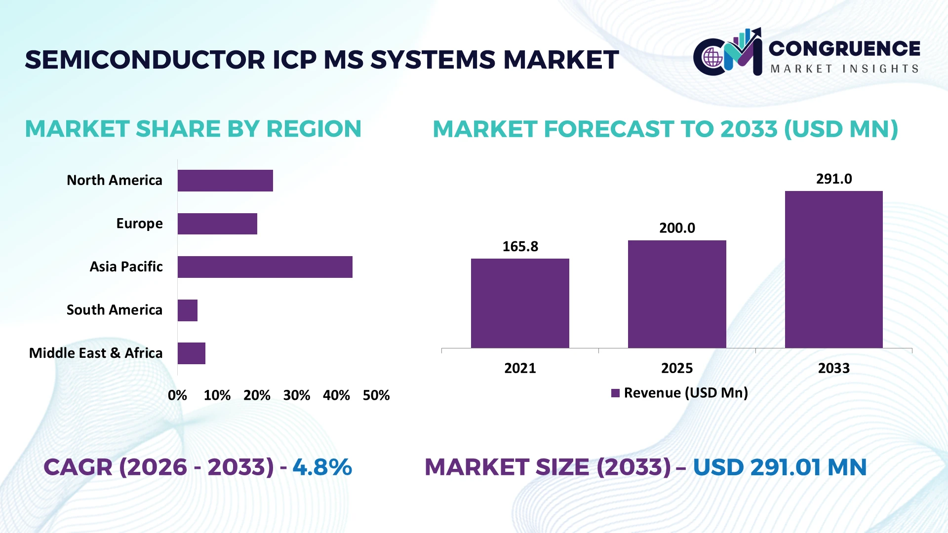
The Global Semiconductor ICP-MS Systems Market was valued at USD 200 Million in 2025 and is anticipated to reach a value of USD 291.01 Million by 2033 expanding at a CAGR of 4.8% between 2026 and 2033. Growth is supported by tighter semiconductor contamination thresholds, rising investment in advanced wafer fabrication, and broader deployment of ultra-trace elemental analysis for sub-5 nm process control.
China accounts for approximately 31% of global semiconductor manufacturing capacity, supported by multi-billion-dollar fab investments and accelerated localization initiatives, while Taiwan contributes nearly 23% through advanced foundry production with high-purity analytical workflows exceeding 90% adoption in leading fabrication facilities. Ongoing technology restrictions and supply-chain realignment in 2026 continue to influence procurement strategies and analytical equipment deployment across Asia, strengthening demand for precision ICP-MS systems. Strategic investment should prioritize high-capacity semiconductor manufacturing hubs where advanced contamination control directly enhances production quality and competitiveness.
Market Size & Growth: USD 200 Million in 2025, reaching USD 291.01 Million by 2033 at 4.8% CAGR, driven by advanced semiconductor contamination control requirements.
Top Growth Drivers: Ultra-trace impurity testing demand rises 18%, advanced wafer production expands 15%, and process quality investments increase 12%.
Short-Term Forecast: By 2028, analytical testing efficiency improves 22% while contamination-related inspection costs decline 14% through automation.
Emerging Technologies: AI-driven data interpretation, automated sample handling, and high-sensitivity quadrupole ICP-MS improve laboratory productivity by over 20%.
Regional Leaders: Asia Pacific exceeds USD 145 Million with fab expansion, North America surpasses USD 63 Million through R&D investment, Europe reaches USD 46 Million via advanced chip initiatives.
Consumer/End-User Trends: More than 68% of leading semiconductor laboratories prioritize ultra-low detection limit analytical platforms for process validation.
Pilot/Case Example: In 2026, automated semiconductor contamination testing reduced analytical turnaround time by 28% in a high-volume fabrication environment.
Competitive Landscape: Top manufacturers hold approximately 57% market share, led by Agilent Technologies, Thermo Fisher Scientific, PerkinElmer, Shimadzu Corporation, and Analytik Jena.
Regulatory & ESG Impact: Chemical waste optimization programs reduce laboratory reagent consumption by nearly 16%, aligning with stricter manufacturing sustainability targets.
Investment & Funding: More than USD 8 Billion in semiconductor ecosystem investments support laboratory modernization amid ongoing global supply-chain diversification.
Innovation & Future Outlook: Next-generation high-throughput ICP-MS platforms and digital laboratory integration strengthen precision analytics for advanced semiconductor manufacturing.
Semiconductor ICP-MS systems are witnessing stronger adoption across advanced wafer fabrication, specialty chemicals, ultrapure water monitoring, and semiconductor materials qualification. AI-assisted analytical software, automated sample preparation, and lower detection-limit instrumentation improve laboratory throughput by nearly 20%. As manufacturers strengthen supply-chain resilience and comply with tighter process quality requirements, precision elemental analysis is becoming a core strategic capability, setting the stage for broader competitive evaluation.
Semiconductor ICP-MS systems are becoming strategically important as chipmakers tighten contamination control standards for advanced process nodes and strengthen resilient manufacturing ecosystems. Supply-chain restructuring across Asia and North America is accelerating investments in localized analytical laboratories that support high-purity chemical qualification and wafer process verification. As semiconductor fabrication shifts toward sub-5 nm technologies, elemental detection accuracy has become a competitive differentiator for yield optimization and production consistency.
Modern ICP-MS platforms equipped with automated sample handling and AI-assisted data processing deliver nearly 30% faster analytical workflows while reducing manual intervention by approximately 25% compared with conventional laboratory systems. Taiwan continues to lead high-volume deployment through advanced foundries, whereas the United States is emphasizing domestic analytical infrastructure linked to semiconductor manufacturing expansion. Over the next two to three years, automation penetration in semiconductor analytical laboratories is expected to exceed 70%, improving testing consistency and reducing operational bottlenecks.
A leading wafer fabrication facility integrating automated ICP-MS contamination monitoring achieved a 20% reduction in process qualification time, enabling faster production releases. Equipment manufacturers are expanding application-specific product portfolios, strengthening software partnerships, and investing in digital laboratory integration. Companies securing scalable analytical capabilities alongside localized technical support will establish stronger competitive positioning and long-term operational resilience.
Advanced semiconductor manufacturing increasingly requires elemental detection at ultra-trace levels, making high-performance ICP-MS systems essential for process qualification. More than 85% of leading fabrication facilities now integrate contamination monitoring across multiple production stages, while automated analytical workflows improve laboratory productivity by nearly 24% and reduce retesting by approximately 18%. China's continued investment in domestic semiconductor production has expanded demand for localized analytical infrastructure and precision metrology. In response, instrument manufacturers are expanding cleanroom-compatible product lines, establishing regional application centers, and collaborating with semiconductor material suppliers. This transition strengthens process yield, reduces manufacturing variability, and creates a sustainable competitive advantage through superior quality assurance.
The adoption of semiconductor ICP-MS systems remains constrained by high acquisition costs, complex installation requirements, and dependence on specialized components. Imported precision parts account for nearly 40% of critical instrument assemblies, while calibration and validation activities can represent over 15% of annual operating expenses. Export control measures affecting analytical technologies have extended procurement cycles in several manufacturing markets, delaying laboratory expansion projects. Companies are responding by localizing selected component production, negotiating long-term supplier agreements, and qualifying multiple sourcing partners. These measures improve procurement stability while reducing operational exposure to international supply disruptions and cost volatility.
Digital transformation is creating new opportunities through AI-enabled laboratory management, predictive maintenance, and integrated semiconductor quality platforms. Intelligent workflow automation reduces analytical turnaround time by approximately 28%, while cloud-connected laboratory systems improve equipment utilization by nearly 20%. Japan is accelerating investment in smart semiconductor manufacturing infrastructure, encouraging broader adoption of digitally connected analytical instruments. Equipment suppliers are strengthening software capabilities, expanding collaborative research programs, and developing application-specific analytical packages for advanced materials. The combination of digital analytics with ultra-sensitive elemental measurement enables manufacturers to optimize production quality while supporting faster qualification of next-generation semiconductor processes.
Maintaining consistent analytical performance across expanding semiconductor manufacturing networks remains a significant execution challenge. Laboratories processing advanced-node materials experience sample volumes increasing by approximately 25%, while the availability of experienced ICP-MS specialists has improved by less than 10%, creating operational bottlenecks. The growing integration of laboratory information systems with factory automation also increases validation complexity and cybersecurity requirements. Manufacturers are investing in workforce development, standardized digital workflows, remote diagnostics, and collaborative service partnerships to improve deployment consistency. Organizations that successfully combine technical expertise with scalable analytical infrastructure will achieve stronger manufacturing reliability and long-term competitive differentiation.
AI-Driven Laboratory Automation Advanced semiconductor laboratories are increasing AI-enabled analytical workflow adoption, with automated sample preparation expanding by nearly 34% and reporting time declining by 27%. Labor shortages and higher production complexity are accelerating this transition. Instrument vendors are integrating intelligent software, predictive diagnostics, and robotic handling systems to improve throughput while reducing manual quality-control variability.
Localized Supply Network Expansion Semiconductor manufacturers are restructuring procurement strategies as domestic sourcing programs strengthen across the United States, Japan, and South Korea. Regional sourcing of analytical consumables has increased by approximately 22%, while inventory lead times have declined by nearly 18%. Equipment suppliers are expanding local service centers, technical partnerships, and application laboratories to improve installation speed and customer support resilience.
Higher-Purity Materials Verification Growing adoption of advanced process nodes has increased ultra-trace contamination testing frequencies by nearly 30%, while qualification cycles have shortened by about 16%. Manufacturers are standardizing high-sensitivity ICP-MS workflows for chemicals, process gases, and ultrapure water. Companies are expanding dedicated semiconductor application packages to improve repeatability and accelerate production qualification without disrupting fabrication schedules.
Integrated Smart Fab Connectivity More than 60% of newly commissioned semiconductor analytical laboratories now connect ICP-MS platforms with manufacturing execution systems and digital quality dashboards. Real-time process visibility reduces investigation time by approximately 21% while improving production traceability. Equipment manufacturers are strengthening software interoperability, cybersecurity capabilities, and enterprise partnerships as digital factory strategies become operational priorities.
Quadrupole ICP-MS remains the leading segment, accounting for approximately 48% of market deployment due to its balance of analytical sensitivity, operating cost, and compatibility with routine semiconductor contamination testing. Its scalability across wafer manufacturing, chemical verification, and ultrapure water analysis supports widespread deployment in high-volume fabrication facilities. High-Resolution ICP-MS retains strategic importance for complex elemental characterization, while Multi-Collector ICP-MS serves specialized isotope ratio applications with relatively limited commercial deployment. Manufacturers continue enhancing quadrupole platforms through automation, software integration, and contamination-resistant sample introduction systems.
Triple Quadrupole ICP-MS represents the fastest-growing segment as advanced semiconductor manufacturing demands lower detection limits and superior interference removal. Adoption has increased by nearly 24% among advanced process laboratories, while automated analytical workflows improve productivity by approximately 20%. Equipment suppliers are prioritizing product innovation, application-specific configurations, and collaborative development with semiconductor manufacturers. Investment priorities increasingly favor flexible analytical platforms capable of supporting future process technologies while maintaining high laboratory utilization and operational consistency.
Wafer Analysis leads the market with an estimated 36% share because contamination directly influences device yield, process stability, and production qualification. High-volume semiconductor facilities increasingly perform continuous elemental verification throughout manufacturing, strengthening demand for automated analytical systems. Chemical Purity Testing remains a critical supporting application for validating process chemicals, while Ultra-Trace Metal Analysis continues expanding alongside advanced node manufacturing requiring extremely low contamination thresholds.
Process Control is the fastest-growing application as semiconductor manufacturers integrate analytical data into digital production environments. Deployment of automated contamination monitoring has increased by approximately 26%, while real-time analytical feedback improves process consistency by nearly 19%. Failure Analysis continues supporting advanced packaging and complex device diagnostics, although its deployment is generally targeted rather than continuous. Equipment providers are expanding software integration, laboratory automation, and customized application solutions to strengthen analytical efficiency and accelerate manufacturing decision-making.
Semiconductor Manufacturers account for approximately 46% of total demand because they operate extensive contamination monitoring infrastructure supporting every stage of wafer production. Continuous investment in advanced fabrication facilities and process qualification strengthens purchasing activity for high-performance ICP-MS systems. Foundries represent the second-largest buyer group, emphasizing standardized analytical workflows that maintain customer quality requirements across diverse manufacturing programs. Vendors increasingly deliver customized software, validation services, and long-term maintenance agreements to strengthen customer retention.
Semiconductor Research Institutes are the fastest-growing end-user segment as governments and enterprises accelerate research into next-generation materials and advanced process technologies. Analytical instrument deployment within research environments has expanded by nearly 22%, while collaborative laboratory programs have increased by approximately 18%. Analytical Testing Laboratories continue broadening outsourced semiconductor testing capabilities to support smaller manufacturers lacking dedicated analytical infrastructure. Equipment suppliers are strengthening ecosystem partnerships, flexible pricing models, and application-focused product development to address evolving purchasing priorities across both commercial and research environments.
Asia-Pacific accounted for the largest market share at 52.8% in 2025 however, North America is expected to register the fastest growth, expanding at a 5.4% between 2026 and 2033.
Domestic Semiconductor Investment Accelerates Analytical Infrastructure
North America remains a high-value market for semiconductor ICP-MS systems, supported by large-scale semiconductor manufacturing investments, advanced research laboratories, and expanding domestic supply chains. The region represents approximately 24% of global demand, with analytical instrument deployment concentrated in advanced fabrication facilities and semiconductor materials testing laboratories. Increased localization of semiconductor production has accelerated installation of contamination-monitoring laboratories, while automated elemental analysis deployment has expanded by nearly 21% across newly commissioned facilities. Strategic partnerships between analytical instrument manufacturers and semiconductor producers continue strengthening laboratory productivity through integrated software platforms and automated sample preparation. Companies are also expanding field service networks and technical application centers to improve equipment uptime and customer support for advanced manufacturing operations.
United States Market Outlook: The United States leads regional demand through substantial semiconductor manufacturing expansion, national technology initiatives, and strong research infrastructure. More than 70% of regional semiconductor analytical laboratories are located within the country, supported by advanced wafer fabrication and specialty materials production. Equipment suppliers continue investing in local demonstration laboratories, application engineering teams, and digital service capabilities to strengthen customer engagement and accelerate deployment across next-generation semiconductor manufacturing programs.
Precision Manufacturing and Sustainability Shape Adoption
Europe maintains a strategic position through advanced semiconductor materials research, specialty chip manufacturing, and strict quality assurance standards. The region contributes approximately 18% of global deployment, with Germany, France, and the Netherlands driving demand for high-sensitivity elemental analysis. Increased investment in semiconductor manufacturing resilience has expanded laboratory modernization projects by nearly 17%, while automated contamination monitoring has improved operational efficiency across advanced production environments. Instrument manufacturers are strengthening partnerships with research institutions and semiconductor equipment suppliers while integrating digital laboratory management capabilities that support compliance, traceability, and process optimization.
Germany Market Outlook: Germany serves as the region's primary semiconductor manufacturing and industrial technology hub, supported by strong engineering capabilities and specialty materials expertise. Analytical laboratory investments continue expanding alongside semiconductor ecosystem development, while automated quality-control deployment has increased by approximately 20% within advanced manufacturing facilities. Local collaboration between equipment suppliers, industrial enterprises, and research organizations strengthens innovation and supports precision semiconductor process qualification.
Manufacturing Scale Drives Analytical Leadership
Asia-Pacific dominates the Semiconductor ICP-MS Systems Market through its concentration of semiconductor fabrication plants, materials suppliers, and advanced electronics manufacturing ecosystems. The region accounts for approximately 53% of global demand, supported by large-scale wafer production and sustained investments in contamination-control infrastructure. More than 65% of newly installed semiconductor analytical laboratories are located within major manufacturing economies across the region. Equipment suppliers continue expanding localized manufacturing, technical support centers, and application laboratories while strengthening strategic partnerships with foundries and semiconductor material producers. Digital laboratory integration and automated contamination testing are becoming standard operational requirements for advanced fabrication facilities.
China Market Outlook: China remains the largest national market because of continuous semiconductor manufacturing expansion, localized supply-chain development, and increasing investment in analytical infrastructure. Domestic semiconductor production initiatives have accelerated deployment of precision elemental analysis systems, while localized procurement of analytical equipment has increased by approximately 24%. Manufacturers are strengthening regional production capabilities and technical support services to improve supply reliability and accelerate customer adoption.
Emerging Electronics Ecosystems Expand Demand
South America represents an emerging market where semiconductor analytical capability is expanding alongside electronics manufacturing, industrial laboratories, and imported semiconductor component processing. The region contributes approximately 3.8% of global deployment, with Brazil accounting for the largest share of laboratory installations. Investments in advanced laboratory infrastructure have increased by nearly 14%, supporting greater adoption of contamination testing for electronics manufacturing and industrial materials. International analytical equipment suppliers are strengthening distributor partnerships, technical training programs, and localized service capabilities to improve customer access while addressing infrastructure limitations and specialized workforce availability.
Brazil Market Outlook: Brazil leads regional adoption through its established electronics manufacturing sector, industrial testing infrastructure, and expanding research capabilities. Semiconductor-related analytical laboratories continue modernizing contamination testing processes, while automated elemental analysis deployment has increased by approximately 16% across major industrial laboratories. Equipment vendors are expanding technical support partnerships and application training to improve operational efficiency and long-term equipment utilization.
Technology Infrastructure Investment Supports Market Development
The Middle East & Africa market is developing through increasing investment in advanced laboratories, electronics research, and industrial diversification strategies. The region contributes approximately 1.4% of global deployment, with demand concentrated in technology research centers and specialized analytical laboratories. Government-supported laboratory modernization initiatives have increased analytical infrastructure investment by nearly 15%, encouraging wider adoption of precision elemental analysis. Equipment suppliers are strengthening regional partnerships, expanding service capabilities, and supporting laboratory workforce development to improve operational readiness and long-term technology utilization.
Saudi Arabia Market Outlook: Saudi Arabia leads regional momentum through industrial diversification, research infrastructure expansion, and investment in advanced analytical laboratories. National technology initiatives continue strengthening semiconductor-related research capabilities, while deployment of high-precision analytical instrumentation has increased by approximately 18% within government-supported laboratories. Companies are expanding technical collaboration, training, and localized service operations to support long-term analytical capability development.
The market is led by Agilent Technologies, Thermo Fisher Scientific, Shimadzu Corporation, PerkinElmer, and Analytik Jena, competing against specialized analytical instrument innovators and regional precision equipment suppliers. The top five players collectively control approximately 57% of global market activity. Competition centers on analytical sensitivity, software automation, contamination detection capability, service response, and application customization rather than price alone. Automated workflow integration improves laboratory productivity by nearly 25%, while AI-enabled analytical software reduces reporting time by approximately 20%, creating measurable differentiation. Global leaders strengthen positions through product innovation, semiconductor-focused application laboratories, strategic partnerships with chip manufacturers, and localized service expansion. Regional suppliers compete through faster customization, flexible support, and shorter delivery cycles. Increasing digital laboratory integration and stricter semiconductor quality standards are raising technology barriers for new entrants. Sustainable success requires advanced contamination detection performance, integrated digital workflows, strong semiconductor partnerships, rapid technical support, and continuous innovation aligned with evolving fabrication requirements.
Agilent Technologies
Thermo Fisher Scientific
Shimadzu Corporation
PerkinElmer
Analytik Jena
HORIBA Ltd.
Hitachi High-Tech Corporation
Nu Instruments Ltd.
Spectro Analytical Instruments GmbH
GBC Scientific Equipment
Teledyne CETAC Technologies
Aurora Biomed Inc.
Rigaku Corporation
Skyray Instrument Inc.
Semiconductor ICP-MS systems are rapidly advancing through AI-assisted data processing, automated sample preparation, and high-sensitivity triple quadrupole architectures that improve contamination monitoring for advanced wafer fabrication. Automated workflows increase laboratory productivity by approximately 24%, while intelligent interference correction improves analytical consistency by nearly 18%. More than 68% of newly commissioned semiconductor analytical laboratories now deploy integrated digital workflow software, enabling faster qualification of high-purity chemicals and ultrapure water. These technologies reduce manual intervention, strengthen process repeatability, and support higher manufacturing yields across leading semiconductor production facilities.
Emerging technologies include cloud-connected laboratory management, predictive maintenance, and semiconductor-specific analytical software integrated with manufacturing execution systems. Real-time instrument diagnostics reduce unexpected downtime by nearly 16%, while automated calibration lowers routine operating effort by approximately 20%. Compared with conventional single quadrupole workflows, modern triple quadrupole platforms deliver over 30% faster analytical throughput with superior interference removal, enabling more reliable ultra-trace elemental detection. Advanced foundries and high-volume chip manufacturers gain the greatest competitive advantage through faster process qualification and reduced production variability.
Between 2026 and 2028, digital laboratory integration, robotics, and AI-enabled quality analytics will become standard across next-generation semiconductor manufacturing. Equipment vendors expanding software ecosystems, automation partnerships, and semiconductor-focused application platforms will strengthen competitive positioning as contamination control evolves into a core operational differentiator rather than a laboratory function.
May 2026 Agilent Technologies launched the Agilent 9500 Triple Quadrupole ICP-MS featuring Air Cell technology and Advanced Helium Mode, delivering more than 33% faster acquisition time while simplifying interference removal for advanced trace analysis. This strengthens semiconductor contamination testing productivity.
June 2025 Agilent Technologies released ICP-MS MassHunter 5.4 software with dedicated semiconductor reagent workflows, SEMI E30 SDK integration, and enhanced nanoparticle analysis, improving workflow automation and Windows 11 compatibility for advanced laboratories.
May 2026 Agilent Technologies introduced OpenLab Sync to enable guided digital laboratory execution, improving workflow standardization and laboratory connectivity across analytical environments. The platform strengthens enterprise-scale data management and operational consistency for high-throughput semiconductor laboratories. Source: (https://www.agilent.com)
May 2026 Agilent Technologies expanded its spectroscopy portfolio at ASMS 2026 by showcasing integrated mass spectrometry and chromatography solutions, reinforcing connected laboratory workflows and accelerating analytical productivity through broader platform integration for advanced industrial applications. Source: (https://www.agilent.com)
This report provides a comprehensive assessment of the Semiconductor ICP-MS Systems Market across key technology categories, operational trends, and strategic industry developments between 2026 and 2033. It evaluates four product types, five core application areas, and four end-user groups while covering major markets across North America, Europe, Asia-Pacific, South America, and the Middle East & Africa. The analysis also examines deployment patterns, laboratory automation trends, contamination-control requirements, and digital integration across advanced semiconductor manufacturing environments.
The report benchmarks leading manufacturers, competitive positioning, technology adoption, and regional deployment dynamics using operational indicators and segment-level insights. It highlights evolving demand for high-sensitivity analytical platforms, automation-ready laboratory systems, and semiconductor-specific software integration, with more than 65% of advanced fabrication facilities prioritizing digital analytical workflows. The findings support investment planning, capacity expansion, partnership evaluation, product development, and long-term competitive strategy by identifying high-value opportunities, emerging technology priorities, and evolving enterprise procurement trends.
| Report Attribute/Metric | Report Details |
|---|---|
Market Revenue in 2025 | USD 200 Million |
Market Revenue in 2033 | USD 291.01 Million |
CAGR (2026 - 2033) | 4.8% |
Base Year | 2025 |
Forecast Period | 2026 - 2033 |
Historic Period | 2021 - 2025 |
Segments Covered | By Type
By Application
By End-User
|
Key Report Deliverable | Revenue Forecast, Growth Trends, Market Dynamics, Segmental Overview, Regional and Country-wise Analysis, Competition Landscape |
Region Covered | North America, Europe, Asia-Pacific, South America, Middle East, Africa |
Key Players Analyzed | Agilent Technologies, Thermo Fisher Scientific, Shimadzu Corporation, PerkinElmer, Analytik Jena, HORIBA Ltd., Hitachi High-Tech Corporation, Nu Instruments Ltd., Spectro Analytical Instruments GmbH, GBC Scientific Equipment, Teledyne CETAC Technologies, Aurora Biomed Inc., Rigaku Corporation, Skyray Instrument Inc. |
Customization & Pricing | Available on Request (10% Customization is Free) |