
Reports
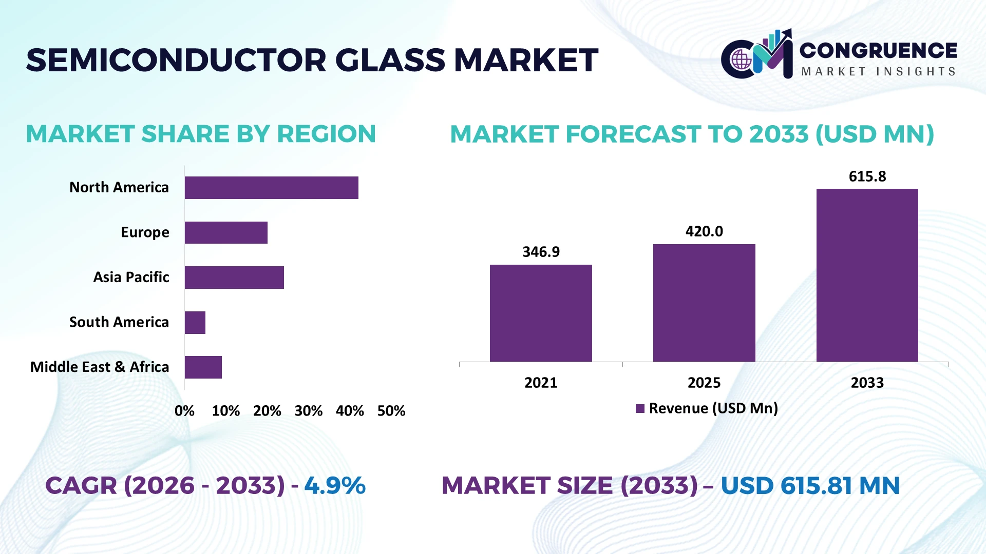
The Global Semiconductor Glass Market was valued at USD 420 Million in 2025 and is anticipated to reach a value of USD 615.81 Million by 2033 expanding at a CAGR of 4.9% between 2026 and 2033. Growth is driven by AI/HPC chiplet packaging, TGV-enabled glass cores, EUV photomask blanks, and the shift from organic substrates toward larger, lower-warpage advanced packages.
Japan dominates the specialty semiconductor-glass supply base, supported by major glass manufacturers and advanced semiconductor applications, with EUV photomask-blank sales growing about 50% year over year. Japan is also strengthening semiconductor capacity through major foundry investments, while Taiwan remains the leading hub for advanced foundry and packaging activity. Japan’s 515 × 510 mm glass-core development contrasts with Taiwan’s concentrated foundry ecosystem, with Japan, Taiwan, and mainland China collectively accounting for more than 80% of projected panel-level packaging capacity by 2030.
Strategically, suppliers prioritizing Japan-Taiwan packaging corridors, TGV processing, and large-panel glass capacity gain stronger positioning as AI-driven packaging localization accelerates.
Market Size & Growth: USD 420 million in 2025 to USD 615.81 million by 2033 at 4.9% CAGR, driven by advanced AI/HPC packaging.
Top Growth Drivers: AI/HPC packaging 45.6%; interconnect-density potential 10×; pattern-distortion reduction 50%.
Short-Term Forecast: By 2030, glass substrates target up to 50% higher die content per package area versus conventional organic designs.
Emerging Technologies: TGV, glass-core substrates, AI-driven inspection, and co-packaged optics are accelerating advanced semiconductor packaging.
Regional Leaders: Asia Pacific reaches approximately USD 856.24 million, North America USD 360.83 million, and Europe USD 296.11 million, with AI packaging strengthening adoption.
Consumer/End-User Trends: AI servers, data centers, graphics processors, and HPC systems represent the earliest high-value applications for semiconductor glass.
Pilot/Case Example: 2023 glass-substrate demonstrations achieved approximately 50% lower pattern distortion and up to 10× higher interconnect-density potential.
Competitive Landscape: AGC holds approximately 21.5% share, alongside Corning, SCHOTT, HOYA, and Plan Optik across advanced semiconductor-glass applications.
Regulatory & ESG Impact: U.S. semiconductor incentives include USD 75 million for a USD 343 million glass-substrate facility, strengthening domestic supply resilience.
Investment & Funding: Approximately USD 175 million in combined manufacturing and R&D support is accelerating U.S. glass-substrate commercialization and supply-chain localization.
Innovation & Future Outlook: 515 × 510 mm panels, embedded components, ultra-fine vias, and optical integration are shifting competition toward high-density, large-format semiconductor packaging.
The Semiconductor Glass Market is gaining demand from AI accelerators, HPC processors, HBM integration, advanced sensors, and EUV lithography, where dimensional stability and high-density interconnects directly influence package performance. Glass substrates offer up to 10× higher interconnect-density potential than conventional organic substrates, strengthening their role in next-generation semiconductor packaging. A major emerging trend is the transition toward TGV glass cores and large-panel processing as chiplet architectures expand. Japan and Taiwan are strengthening regional semiconductor supply chains, while U.S. manufacturing projects are supporting domestic advanced-packaging material capacity. This shift is increasing emphasis on qualification, precision processing, and scalable panel manufacturing, setting up the market for deeper strategic investment in advanced semiconductor glass technologies.
Semiconductor glass is becoming strategically important because advanced packaging is shifting from conventional organic substrates toward materials capable of supporting higher interconnect density, larger package dimensions, and lower warpage. Glass substrates offer up to 10× higher interconnect-density potential and approximately 50% lower pattern distortion than conventional approaches. This performance advantage is strengthening investment interest as AI accelerators, HBM, chiplets, and high-performance computing increase packaging complexity. The next 2–3 years will prioritize qualification, pilot production, and high-volume manufacturing readiness.
Supply-chain restructuring is further changing competitive priorities. Japan is advancing large-format glass-core development, while Taiwan is concentrating foundry and advanced-packaging capabilities and the United States is expanding domestic substrate manufacturing. Japan’s development of 515 × 510 mm glass panels demonstrates the industry's movement toward larger processing formats. Companies are therefore shifting capital toward TGV fabrication, precision drilling, surface treatment, inspection automation, and strategic partnerships rather than relying exclusively on conventional substrate capacity.
A practical deployment pathway is AI/HPC packaging, where glass cores can support finer interconnect architectures and dimensional stability. Over the next 2–3 years, commercial progress will depend on achieving consistent yields at panel scale and integrating glass with existing assembly equipment. Companies securing qualification partnerships with foundries and OSATs can strengthen supply-chain positioning, reduce commercialization friction, and establish operational advantages before broad deployment.
AI and HPC packaging is accelerating semiconductor-glass adoption as advanced processors require higher interconnect density and tighter dimensional control. Glass substrates provide up to 10× higher interconnect-density potential and approximately 50% lower pattern distortion, while large-format designs target substantially greater package integration. Japan is expanding glass-core development alongside advanced semiconductor investments, while Taiwan continues strengthening sophisticated packaging capacity. The shift from organic substrates toward glass directly increases demand for TGV processing, precision lithography, and automated inspection. Companies are responding through pilot lines, technology partnerships, and process-development investments. The non-obvious advantage is not simply density: lower warpage improves alignment consistency across larger packages, potentially reducing downstream assembly rework and improving manufacturing economics.
High-precision glass processing remains constrained by equipment intensity, yield sensitivity, and specialized material requirements. TGV formation and ultra-fine patterning require tight dimensional control, while approximately 50% lower pattern distortion targets introduce demanding process specifications. Large-format 515 × 510 mm panels also increase handling and defect-management complexity compared with smaller substrates. Japan’s specialized manufacturing base provides strong technical capabilities, but global supply remains concentrated among relatively few qualified suppliers. These conditions can increase qualification cycles and limit rapid capacity scaling. Companies are reducing exposure through multi-supplier qualification, localized processing partnerships, long-term material contracts, and incremental capacity expansion. The key operational issue is yield economics: high theoretical performance does not translate into commercial advantage until defect rates remain consistently low at production scale.
Large-panel processing creates an opportunity to improve packaging productivity while supporting increasingly complex AI and chiplet architectures. Glass substrates offer up to 10× higher interconnect-density potential, while 515 × 510 mm panel development demonstrates a pathway toward substantially larger manufacturing formats. Automated optical inspection, laser-based TGV formation, and advanced surface treatments can further improve process consistency by targeted double-digit percentages. Japan is positioned to commercialize precision glass technologies, while U.S. investments create opportunities for localized advanced-substrate production. Companies are expanding R&D around glass-core architectures and forming partnerships with semiconductor manufacturers and packaging specialists. A less obvious opportunity is integrating optical interconnects with glass platforms, potentially positioning glass as a broader infrastructure layer for high-bandwidth AI systems rather than only a substrate material.
Commercial scaling requires manufacturers to solve process integration across glass preparation, TGV formation, metallization, lithography, inspection, and semiconductor assembly. A 10× interconnect-density potential increases design flexibility but also raises alignment and defect-control requirements, while 515 × 510 mm panels amplify the consequences of localized defects. Automated inspection must therefore achieve extremely consistent detection across large surfaces without slowing throughput. Workforce specialization is another constraint because glass-core processing combines semiconductor fabrication with precision materials engineering. Companies must invest in integrated process-control systems, workforce training, equipment qualification, and joint development programs with OSATs and foundries. The strategic challenge is achieving stable panel-level yields while maintaining compatibility with existing packaging infrastructure, making manufacturing integration as important as material performance for long-term competitiveness.
Glass-Core Commercialization Accelerates Intel and packaging suppliers are moving glass from laboratory validation toward qualification, with 10× interconnect-density potential and 50% lower pattern distortion versus organic substrates. Large-format panel trials are increasing process automation and precision inspection, shifting spending toward yield engineering rather than basic material development.
Precision Processing Gains Priority TGV formation, laser drilling, thin-film metallization, and automated optical inspection are becoming integrated workflows. Targeting 20–30% faster inspection cycles and 10–15% lower handling losses is pushing suppliers toward equipment partnerships. The non-obvious shift is that defect detection, rather than glass availability, increasingly determines usable panel throughput.
AI Packaging Reshapes Demand AI and data-center packages are becoming early deployment targets because glass supports larger form factors and tighter interconnect layouts. Intel’s 2026 collaboration with Lens Technology combines precision glass processing with advanced packaging expertise, showing how partnerships are replacing standalone development models and accelerating manufacturing readiness.
Supply Chains Become Localized U.S. semiconductor incentives and Asian packaging concentration are encouraging localized substrate ecosystems. Companies are targeting 15–20% shorter qualification and logistics cycles through regional supplier networks, dual sourcing, and co-development agreements. This restructuring reduces dependency exposure while creating new demand for specialized glass-processing capacity and regional technical teams.
Quartz Glass is estimated to lead the type segmentation with approximately 34% share, supported by high-purity requirements, thermal stability, chemical resistance, and established integration across semiconductor processing. Fused Silica follows at roughly 29%, benefiting from optical performance and established photomask-related applications. Borosilicate Glass holds around 17%, with cost and thermal characteristics supporting mature industrial uses, while Aluminosilicate Glass accounts for approximately 11% and remains relevant where mechanical strength is prioritized. Specialty Glass represents about 9% but is expanding fastest as customized compositions address advanced packaging, optical coupling, and high-temperature processing requirements. Companies are reallocating product development toward specialty formulations and tighter purity specifications, while established suppliers continue optimizing quartz and fused-silica capacity. The key investment shift is toward differentiated glass grades rather than commodity-volume expansion.
Semiconductor Wafers are estimated to represent approximately 33% of application demand, supported by high-volume processing, stringent purity requirements, and established semiconductor manufacturing workflows. Photomasks contribute nearly 23%, where optical clarity, dimensional stability, and defect control remain critical. Glass Substrates account for about 21% but represent the fastest-changing application as AI and HPC packaging move toward larger packages and higher interconnect density. Insulating Components hold roughly 10%, while Semiconductor Packaging represents approximately 13% and is gaining strategic importance as chiplet architectures expand. Companies are increasing automation around inspection, laser processing, and surface treatment while building qualification programs with packaging customers. The operational implication is a gradual shift from traditional wafer and photomask volumes toward higher-value substrate and packaging applications requiring tighter process integration.
Semiconductor Manufacturers are estimated to lead end-user demand with approximately 35% share because they control high-volume process qualification and require consistent glass performance across fabrication and packaging workflows. Foundries account for around 24% and represent the fastest-expanding buyer group as heterogeneous integration and advanced packaging become more closely linked to foundry services. Integrated Device Manufacturers contribute nearly 20%, supported by vertically integrated process development, while Electronics Manufacturers hold about 13% and Semiconductor Equipment Manufacturers approximately 8%. Buying behavior is shifting from material procurement toward co-engineered specifications, qualification agreements, and long-term technology partnerships. Companies are tailoring glass formulations, processing parameters, and inspection systems to individual manufacturing platforms. The competitive implication is clear: suppliers that integrate directly with foundry and IDM process-development teams can secure earlier qualification and stronger recurring demand than vendors competing primarily on material price.
Asia-Pacific accounted for the largest market share at 43% in 2025 however, North America is expected to register the fastest growth, expanding at a CAGR of 6.1% between 2026 and 2033.

Domestic advanced-packaging capacity reshapes procurement
North America is strengthening its semiconductor-glass position through localized advanced packaging, AI infrastructure, and semiconductor manufacturing expansion. The region accounts for approximately 27% of global demand, with the United States concentrating most deployment across Arizona, Georgia, California, and New York. TSMC’s planned U.S. semiconductor investment of USD 165 billion, including advanced packaging facilities, is increasing demand for high-performance substrate materials and precision glass components. Glass-core qualification programs are also moving closer to commercial production, encouraging suppliers to establish local processing and technical-support capabilities. Companies are prioritizing domestic supply agreements, automation, and joint qualification programs to reduce dependence on Asian production networks.
United States Market Outlook: The United States leads regional investment because of its expanding AI semiconductor ecosystem and advanced-packaging infrastructure. More than 15 major semiconductor fabrication and packaging projects are entering construction or expansion phases, creating stronger demand for precision glass, TGV processing, carriers, and inspection technologies.
Specialty materials gain strategic importance
Europe represents approximately 17% of global semiconductor-glass demand, supported by Germany, France, the Netherlands, and Italy's semiconductor equipment and specialty-material ecosystems. The region's competitive position is centered more on precision materials, photomasks, optical components, and semiconductor equipment than on high-volume packaging. Germany remains particularly important for high-purity glass and specialty-material engineering, while European semiconductor modernization programs are increasing demand for locally qualified components. More than 15 new semiconductor-related facility projects across Europe and the Middle East were identified for construction activity during 2025, strengthening the industrial base for specialized material suppliers. Companies are responding through equipment-material partnerships, advanced inspection, and localized qualification programs.
Germany Market Outlook: Germany provides a strong manufacturing and engineering base for specialty semiconductor glass, supported by established optics, semiconductor-equipment, and industrial-material capabilities. Its position in European semiconductor manufacturing creates demand for high-purity glass components, precision carriers, and process-compatible materials requiring stringent dimensional and thermal specifications.
Manufacturing scale drives glass-core integration
Asia-Pacific commands approximately 43% of semiconductor-glass demand because Japan, Taiwan, South Korea, and China combine semiconductor fabrication, packaging, photomask, and specialty-glass manufacturing capabilities. Taiwan, Japan, and mainland China are projected to account for 84.8% of global panel-level packaging capacity by 2030, reinforcing the region's manufacturing concentration. Japan is advancing large-format glass-core development, while Taiwan is expanding advanced packaging infrastructure around AI and HPC applications. South Korea is increasing investment in glass-core technologies through semiconductor-packaging partnerships. Companies are responding with localized TGV capacity, automated inspection, large-panel development, and joint ventures with foundries and OSAT providers.
Japan Market Outlook: Japan holds a strategically important position through advanced glass chemistry, photomask materials, precision manufacturing, and semiconductor-equipment integration. AGC is developing 515 × 510 mm glass-core panels and microvia structures, strengthening Japan's position in large-format packaging and creating opportunities for suppliers specializing in high-purity materials and precision processing.
Industrial modernization creates selective demand
South America represents approximately 5% of global semiconductor-glass demand, with Brazil accounting for the largest portion through electronics manufacturing, semiconductor assembly, industrial automation, and research infrastructure. Demand remains concentrated around imported semiconductor components, specialized laboratory equipment, and electronics production rather than large-scale glass-core fabrication. Brazil's semiconductor policy framework is encouraging domestic technology development and manufacturing localization, while industrial electronics investment is increasing demand for precision components. Companies are primarily pursuing distributor partnerships, localized technical support, and application-specific supply agreements rather than constructing large dedicated glass facilities. The region's opportunity is therefore tied to downstream integration, where reliable access to qualified materials can shorten procurement cycles and improve manufacturing continuity.
Brazil Market Outlook: Brazil is the most strategically relevant market because of its comparatively large electronics and semiconductor ecosystem. Government-backed semiconductor initiatives and domestic technology programs are strengthening local capabilities, creating demand for specialty glass used in wafers, photomasks, insulating components, and electronics manufacturing infrastructure.
Digital infrastructure drives emerging adoption
Middle East & Africa accounts for approximately 4% of semiconductor-glass demand, with Israel, the United Arab Emirates, and Saudi Arabia forming the strongest technology and infrastructure clusters. Israel's semiconductor design and equipment ecosystem provides specialized demand, while Gulf economies are investing heavily in data centers, AI infrastructure, and digital manufacturing. Saudi Arabia and the UAE are expanding semiconductor-related investment programs and technology partnerships, increasing demand for high-reliability electronic materials. Companies are entering through distribution partnerships, technical alliances, and localized assembly rather than immediate large-scale glass manufacturing. The strategic shift is toward infrastructure-led demand, where semiconductor glass benefits indirectly from AI computing, electronics manufacturing, and advanced equipment deployment.
Israel Market Outlook: Israel remains the region's most technology-intensive semiconductor market because of its established chip-design, equipment, and research ecosystem. Its concentration of semiconductor engineering activity supports demand for high-purity glass components, photomask-related materials, and precision equipment, while technology partnerships provide an efficient route for specialized suppliers.
AGC, Corning, SCHOTT, HOYA, and Plan Optik compete as specialty-glass suppliers, while Toppan, Nippon Electric Glass, and Samsung Electro-Mechanics intensify competition through packaging-specific development and regional capacity. The top five players hold an estimated 72.8% combined share, creating a moderately concentrated structure. Competition centers on glass purity, TGV capability, panel size, qualification speed, and supply reliability rather than price alone. Advanced suppliers target 10× higher interconnect-density potential and approximately 50% lower pattern distortion, while large-panel processing aims to improve material utilization by roughly 15–20%. AGC and SCHOTT emphasize technology differentiation; Corning competes through engineered glass and process integration; Asian players strengthen customer proximity through partnerships and localized manufacturing. The shift is toward glass-core qualification and AI-package integration, with foundry and OSAT relationships becoming decisive. Entry barriers include precision equipment, quality systems, qualification cycles, and defect-control expertise. Winning requires validated TGV performance, scalable yields, diversified supply, and co-development with packaging ecosystems.
AGC Inc.
Corning Incorporated
SCHOTT AG
HOYA Corporation
Plan Optik AG
Nippon Electric Glass Co., Ltd.
Toppan Holdings Inc.
Ohara Inc.
Nippon Sheet Glass Co., Ltd.
Samsung Electro-Mechanics Co., Ltd.
Shilpa Enterprises
SKC Co., Ltd.
Current semiconductor glass technology centers on ultra-flat carrier glass, TGV substrates, and low-expansion photomask glass. Corning carriers can reduce advanced-packaging warpage by up to 40%, while Intel reports 10x higher interconnect density than organic substrates and 50% more die content within the same package area. These gains support larger chiplet architectures and tighter routing. AI and HPC remain primary near-term demand centers, making qualification strategically important before broader commercialization.
Emerging technologies include laser-processed TGVs, large-panel glass cores, and low-loss glass for high-frequency packaging. Nippon Electric Glass has developed 515×510 mm glass-core panels, while SCHOTT’s low-loss glass records dielectric constant 4.0 and dielectric loss tangent 0.0021 at 10 GHz. Deployment remains concentrated in pilot lines, samples, and customer evaluations, creating early supplier-qualification opportunities and manufacturing advantages as process integration advances.
Disruptive integration is moving toward glass cores combined with optical interconnects, advanced inspection, and heterogeneous packaging. Intel and Lens Technology began collaboration in 2026, while Onto Innovation and LPKF integrated process capabilities for panel-level production. Through 2026–2028, these technologies matter because they can improve package density, signal integrity, and dimensional control, giving qualified materials, equipment, and processing suppliers an earlier competitive position across supply chains globally.
May 2025 Nippon Electric Glass developed 515×510 mm GC Core substrates for next-generation semiconductor packages, expanding large-panel capability. The development supports larger chiplet packages while using existing manufacturing equipment, potentially reducing capital requirements and improving mass-production readiness and scale. Source:
December 2025 DNP launched a TGV glass-core substrate pilot line at its Kuki Plant, with sample shipments beginning early 2026. The 510×515 mm platform advances mass-production verification and supports higher via density for next-generation packaging and commercial deployment.
July 2025 RENA Technologies commissioned a dedicated TGV glass-substrate processing facility in Germany for panels up to 510×515 mm. Customer test lots began immediately, enabling process validation and high-aspect-ratio TGV development while expanding European glass-processing capacity and capability.
May 2026 SEMI and Global Net Corp. released a glass-core substrate development report covering AI and HPC packaging, with scenarios indicating initial production around 2028. The research strengthens industry visibility on qualification barriers, supply-chain readiness, and commercialization timing.
The Semiconductor Glass Market Report covers glass types including borosilicate, aluminosilicate, glass-ceramic, fused silica, and specialty low-expansion grades, with segmentation by carrier substrates, TGV glass, glass-core substrates, photomask materials, and related components. Application coverage spans advanced semiconductor packaging, wafer-level and panel-level processing, EUV lithography, high-frequency communication, photonics, AI, HPC, and chiplet architectures. End-user analysis includes semiconductor manufacturers, foundries, OSATs, substrate producers, equipment suppliers, and materials companies.
Regional coverage evaluates North America, Europe, Asia Pacific, Latin America, and the Middle East & Africa, with detailed assessment of leading manufacturing hubs and emerging supply bases. The report tracks technologies such as TGV processing, laser drilling, low-loss glass, glass-core integration, and optical interconnects, alongside niche developments in large-panel packaging. It supports investment planning, capacity expansion, supplier selection, competitive positioning, technology qualification, and market-entry decisions through 2026–2033.
| Report Attribute/Metric | Report Details |
|---|---|
Market Revenue in 2025 | USD 420 Million |
Market Revenue in 2033 | USD 615.81 Million |
CAGR (2026 - 2033) | 4.9% |
Base Year | 2025 |
Forecast Period | 2026 - 2033 |
Historic Period | 2021 - 2025 |
Segments Covered | By Type
By Application
By End-User
|
Key Report Deliverable | Revenue Forecast, Growth Trends, Market Dynamics, Segmental Overview, Regional and Country-wise Analysis, Competition Landscape |
Region Covered | North America, Europe, Asia-Pacific, South America, Middle East, Africa |
Key Players Analyzed | AGC Inc., Corning Incorporated, SCHOTT AG, HOYA Corporation, Plan Optik AG, Nippon Electric Glass Co., Ltd., Toppan Holdings Inc., Ohara Inc., Nippon Sheet Glass Co., Ltd., Samsung Electro-Mechanics Co., Ltd., Shilpa Enterprises, SKC Co., Ltd. |
Customization & Pricing | Available on Request (10% Customization is Free) |