
Reports
The Global Semiconductor Capital Equipment Market was valued at USD 107550 Million in 2025 and is anticipated to reach a value of USD 184790.92 Million by 2033 expanding at a CAGR of 7% between 2026 and 2033. AI accelerators, high-bandwidth memory, 2nm gate-all-around production, advanced packaging, and fab regionalization are driving equipment demand across lithography, deposition, etch, metrology, test, and packaging.
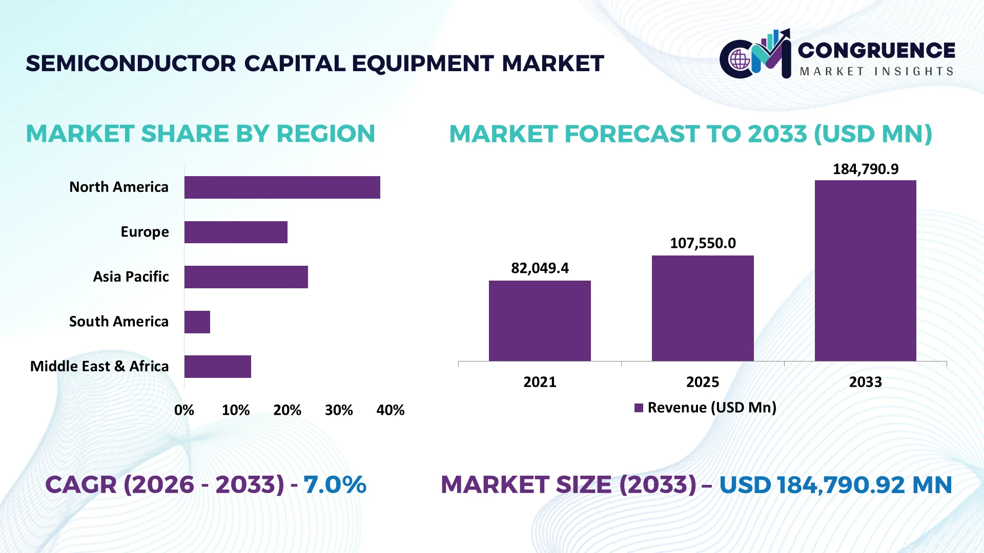
China remained the dominant country market in 2025, accounting for approximately 36.5% of global semiconductor equipment billings with about USD 49.3 billion in purchases, supporting mature-node foundries, power devices, analog chips, and selective advanced capacity. Taiwan's equipment spending increased roughly 90%, compared with about 26% growth in South Korea, as U.S.-led export controls intensified semiconductor localization and supply-chain restructuring across Asia.
The strategic priority is to balance exposure to leading-edge fabs in Taiwan and South Korea with localized product strategies for China's expanding domestic semiconductor manufacturing ecosystem.
Market Size & Growth: USD 107.55 billion in 2025 is projected to reach USD 184.79 billion by 2033 at 7% CAGR, driven by AI-oriented leading-edge fab expansion.
Top Growth Drivers: Test equipment grew approximately 55%, assembly and packaging equipment 21%, and wafer-processing equipment 12%, reflecting rising HBM, AI processor, and advanced-node intensity.
Short-Term Forecast: By 2028, next-generation EUV platforms are targeting roughly 260 wafers per hour versus about 230 currently, supporting approximately 13% higher throughput.
Emerging Technologies: High-NA EUV delivers about 40% greater imaging contrast, while GAA transistors and hybrid bonding increase demand for precision deposition, etch, and metrology systems.
Regional Leaders: China, South Korea, and Taiwan are positioned to direct approximately USD 94 billion, USD 86 billion, and USD 75 billion respectively into 300mm equipment investment during 2026–2028.
Consumer/End-User Trends: China, Taiwan, and South Korea together represented nearly 79% of 2025 semiconductor equipment spending, confirming procurement concentration among foundry and memory manufacturers.
Pilot/Case Example: In 2026, software optimization on advanced EUV systems raised throughput from roughly 220 to 230 wafers per hour, improving installed-tool productivity by about 4.5%.
Competitive Landscape: ASML holds approximately 21% of wafer-fab equipment share, competing with Applied Materials, Lam Research, Tokyo Electron, and KLA across critical process steps.
Regulatory & ESG Impact: Newer EUV platforms have reduced energy consumption per wafer pass by more than 50% versus earlier generations, while export controls continue reshaping equipment availability in China.
Investment & Funding: About USD 374 billion in 300mm fab equipment investment is planned for 2026–2028, driven by AI capacity, advanced memory, and semiconductor localization programs.
Innovation & Future Outlook: High-NA EUV enables features roughly 1.7 times smaller and transistor densities up to 2.9 times higher, shifting investment toward advanced process-control ecosystems.
Semiconductor Capital Equipment Market demand is concentrating around AI processors, HBM, 2nm logic, advanced packaging, and increasingly complex process control. High-NA EUV delivers about 40% greater imaging contrast, while hybrid bonding and AI-enabled metrology reshape back-end and inspection workflows. Export controls and fab localization are simultaneously reorganizing equipment supply chains, setting up a more strategically differentiated competitive environment.
Semiconductor capital equipment has become strategic infrastructure for AI computing, advanced memory, defense electronics, automotive chips, and national technology sovereignty. Supply-chain restructuring is accelerating as the United States, Japan, Europe, China, Taiwan, and South Korea localize fabrication capacity and tighten technology controls. China represented roughly 36.5% of 2025 equipment billings, while Taiwan recorded about 90% spending growth, demonstrating how geopolitical policy now directly redirects equipment deployment.
Technology intensity is simultaneously rising. High-NA EUV provides approximately 40% greater imaging contrast than conventional EUV and supports features about 1.7 times smaller, reducing multi-patterning complexity at advanced nodes. Taiwan leads leading-edge foundry deployment, South Korea concentrates advanced memory investment, while China emphasizes domestic equipment substitution and mature-node capacity. Through 2026–2028, approximately USD 374 billion of 300mm fab-equipment investment is planned globally.
ASML's progression toward EUV throughput of roughly 260 wafers per hour illustrates the industry's focus on extracting more output from capital-intensive tools. Applied Materials, Lam Research, Tokyo Electron, KLA, and ASML are expanding R&D, service capacity, process integration, and customer collaboration. Competitive advantage will increasingly depend on process yield, installed-base productivity, technology sovereignty, and equipment availability rather than tool performance alone.
AI accelerators, high-bandwidth memory, and gate-all-around logic are raising equipment intensity per wafer because advanced devices require additional deposition, etch, inspection, metrology, and packaging steps. Semiconductor test equipment sales increased approximately 55% in 2025, assembly and packaging systems advanced 21%, and wafer-processing equipment increased 12%. Taiwan's aggressive leading-edge expansion reflects demand for 2nm production, while South Korea is concentrating investment around HBM and advanced DRAM. This technology transition increases tool requirements even when wafer volumes remain comparatively stable. Equipment manufacturers are responding through higher-throughput platforms, atomic-scale process control, advanced packaging systems, and deeper co-development with chipmakers. The strategic insight is process-step multiplication: increasing transistor complexity creates equipment demand independently of conventional semiconductor unit-volume expansion.
Technology restrictions are creating structural barriers across semiconductor equipment supply chains, particularly for advanced lithography, deposition, etch, and inspection systems entering China. China still represented approximately 36.5% of global equipment billings in 2025, making restrictions commercially significant for international suppliers. Meanwhile, China accelerated domestic equipment procurement as semiconductor self-sufficiency policies redirected capital toward local alternatives; Taiwan's equipment spending increased approximately 90% during the same period. U.S., Dutch, and Japanese controls on selected advanced manufacturing technologies force suppliers to manage product configurations, licensing, customer eligibility, and service obligations by destination. Companies are diversifying customer exposure, localizing supply chains, and developing market-specific equipment portfolios. The non-obvious restraint is installed-base servicing: restrictions affect not only new tool shipments but also upgrades, spare parts, and lifecycle economics.
Advanced packaging is creating a second equipment-intensity cycle beyond wafer fabrication as AI processors require chiplets, HBM integration, hybrid bonding, through-silicon vias, and increasingly complex thermal architectures. Assembly and packaging equipment sales increased approximately 21% in 2025, while semiconductor test equipment expanded 55%, substantially outpacing traditional process-equipment categories. Taiwan is scaling CoWoS and related advanced-packaging capacity, while South Korea is expanding HBM manufacturing ecosystems. Through 2026–2028, hybrid bonding, wafer-level packaging, glass substrates, and AI-enabled inspection will increase demand for deposition, bonding, metrology, and test platforms. Applied Materials, Lam Research, KLA, Tokyo Electron, and packaging-equipment specialists are expanding R&D and customer partnerships. Strategically, back-end equipment is becoming front-end-like: packaging precision increasingly determines AI-chip performance, yield, and manufacturing economics.
Scaling next-generation fabs requires simultaneous control of equipment uptime, process uniformity, contamination, yield, software integration, and specialist workforce availability. High-NA EUV enables features approximately 1.7 times smaller and transistor densities approaching 2.9 times higher than conventional EUV capabilities, but increasing process complexity raises calibration and metrology requirements. Leading lithography platforms target throughput near 260 wafers per hour, making even 1%–2% availability losses operationally significant across high-utilization fabs. Taiwan's rapid advanced-node expansion and Arizona's new fabrication infrastructure also intensify competition for experienced equipment engineers and technicians. Suppliers must strengthen field-service networks, predictive maintenance, digital twins, remote diagnostics, and workforce partnerships. The strategic challenge is deployment consistency: technological leadership loses economic value when fabs cannot reproduce targeted yield, uptime, and cycle-time performance across multiple manufacturing locations.
Asia Equipment Spending Concentrates Further: China, Taiwan, and South Korea accounted for 79% of 2025 semiconductor equipment spending, up from 74% in 2024. Taiwan spending increased 90%, while South Korea advanced 26%. Suppliers are expanding field-service capacity and local customer support as advanced-node and memory deployments concentrate around Asian manufacturing clusters.
Back-End Equipment Gains Strategic Weight: Test equipment billings increased 55% in 2025, while assembly and packaging equipment rose 21%, reflecting higher verification intensity for AI processors and HBM. Equipment manufacturers are scaling testers, handlers, bonding platforms, and inspection systems as packaging complexity moves performance bottlenecks beyond front-end wafer fabrication.
Advanced Capacity Replaces Broad Expansion: Capacity at 7nm and below is projected to rise from approximately 850,000 wafers monthly in 2024 to 1.4 million by 2028, a 69% increase. Suppliers are prioritizing atomic-layer deposition, advanced etch, EUV support, and process-control technologies rather than treating all fab additions equally.
Fab Localization Alters Supplier Footprints: Eighteen new fabs began construction planning in 2025, including 15 based on 300mm wafers. The Americas and Japan each accounted for four projects. Export controls and localization incentives are pushing equipment companies to restructure service networks, spare-parts inventories, engineering teams, and supplier partnerships closer to new fabrication sites.
Wafer Fabrication Equipment is the leading type, representing approximately 80%–82% of overall semiconductor manufacturing equipment spending when broad front-end systems are considered. Its dominance reflects the capital intensity of lithography, deposition, etch, cleaning, ion implantation, and process-control steps required at advanced nodes. Within this equipment stack, Lithography Equipment remains technologically critical because EUV systems determine patterning capability below 7nm, while Deposition Equipment gains importance as gate-all-around structures and 3D architectures increase the number of atomic-scale film layers.
Testing Equipment is the fastest-growing provided type, with 2025 billings rising approximately 55%, compared with 21% growth for Assembly & Packaging Equipment and 12% for wafer-processing equipment. AI accelerators, HBM, and chiplet architectures require longer test cycles and tighter fault isolation. Equipment suppliers are therefore directing development toward high-parallelism testers, hybrid bonding, precision deposition, and process integration. Capital priorities are shifting from front-end capacity alone toward balanced investment across fabrication, packaging, and validation.
Wafer Processing represents the largest application, accounting for approximately 55%–60% of equipment deployment across the specified categories because virtually every semiconductor device requires repeated thermal, deposition, cleaning, patterning, and surface-treatment cycles. Lithography remains the highest-value individual process within advanced logic fabs, where EUV and emerging High-NA systems reduce patterning dimensions and support sub-3nm production. Thin-Film Deposition is gaining strategic weight as GAA transistors, 3D NAND, and advanced interconnects require additional conformal layers.
Inspection & Testing is the fastest-expanding application, supported by a 55% increase in test equipment billings during 2025. Etching & Cleaning also intensifies as process structures become deeper and more complex, increasing sensitivity to contamination and profile variation. Equipment companies are integrating AI-assisted inspection, atomic-layer deposition, plasma etch control, and closed-loop process analytics. The business implication is clear: equipment demand increasingly follows process complexity rather than wafer volume alone.
Semiconductor Foundries are the leading end-user group, representing approximately 38% of global installed wafer capacity and the strongest concentration of advanced equipment procurement. Foundry capacity reached about 12.6 million wafers per month in 2025, up 10.9%, reflecting expansion by TSMC and Chinese foundry operators. Integrated Device Manufacturers remain major buyers for logic, analog, automotive, and power semiconductors, while Memory Manufacturers concentrate investment in DRAM, HBM, and 3D NAND process tools.
Memory Manufacturers are the fastest-shifting buyer segment as AI changes capacity allocation. DRAM capacity increased approximately 7% in 2025 to 4.5 million wafers monthly, while 3D NAND capacity reached 3.7 million. Outsourced Assembly Providers are increasing purchases of advanced bonding, packaging, and test systems as heterogeneous integration expands, while Research Institutions concentrate on pilot lines and next-generation process development. Suppliers are responding through application-specific platforms, joint development programs, service contracts, and installed-base upgrades targeting each buyer group's process economics.
Asia-Pacific accounted for the largest market share at approximately 86% in 2025 however, North America is expected to register the fastest growth, expanding at a CAGR of approximately 8.1% between 2026 and 2033.
Domestic Fab Build-Out Reshapes Equipment Deployment
North America represented approximately 8% of global semiconductor equipment billings in 2025, with equipment purchases reaching about 10.9 billion across the region. The United States is shifting from an import-dependent semiconductor structure toward localized leading-edge fabrication, advanced packaging, and specialty-chip production. The Americas accounted for four of the 18 semiconductor fabs scheduled to begin construction during 2025, while regional 300mm capacity approached 9% of global installed capacity. Arizona, Texas, New York, and Ohio are becoming major equipment deployment clusters covering lithography, deposition, etch, inspection, and advanced packaging. Suppliers are expanding engineering, spare-parts, and field-service networks around these projects. The operational advantage increasingly comes from proximity: reducing installation, qualification, and maintenance response times materially improves utilization of highly capital-intensive production tools.
United States Market Outlook: The United States is the region's decisive equipment market as TSMC, Intel, Samsung, Micron, GlobalFoundries, and Texas Instruments expand domestic manufacturing footprints. TSMC's Arizona program alone has expanded toward six wafer fabs, two advanced-packaging facilities, and an R&D center, creating sustained demand for leading-edge process tools. Federal semiconductor incentives reinforce localized equipment-service ecosystems and supplier capacity.
Specialty Manufacturing Meets Lithography Leadership
Europe accounted for approximately 2% of global semiconductor equipment billings in 2025 after regional purchases declined about 41% from the previous year, reflecting weak automotive and industrial semiconductor demand. Despite lower near-term equipment absorption, Europe remains strategically important through ASML's lithography leadership, advanced equipment suppliers, automotive semiconductors, power electronics, and emerging fab localization. Europe and the Middle East together are moving toward roughly 7% of worldwide 300mm capacity, compared with 6% earlier in the decade. Germany, France, Ireland, Italy, and the Netherlands anchor production, R&D, and equipment ecosystems. Three new fab projects were scheduled to begin construction across Europe and the Middle East during 2025. Suppliers are concentrating on energy-efficient processes, silicon carbide, mature-node modernization, and equipment capable of supporting both automotive-grade reliability and advanced-node production.
Netherlands Market Outlook: The Netherlands holds disproportionate strategic importance because ASML supplies the world's commercial EUV lithography systems and is deploying High-NA EUV for sub-2nm manufacturing. High-NA platforms deliver approximately 40% higher imaging contrast and enable features about 1.7 times smaller than existing EUV capability. This equipment leadership gives the Dutch ecosystem influence extending far beyond domestic semiconductor-production capacity.
Manufacturing Concentration Defines Global Equipment Demand
Asia-Pacific dominates semiconductor capital equipment deployment, with China, Taiwan, South Korea, and Japan together representing approximately 86% of worldwide 2025 billings. China alone purchased about 36.5% of global equipment, Taiwan represented approximately 23%, South Korea 19%, and Japan 7%. Taiwan's equipment spending increased around 90% during 2025 as 2nm logic, AI accelerators, and advanced packaging moved into large-scale capacity expansion. South Korea recorded approximately 26% growth, driven by HBM and advanced DRAM, while Japan increased about 22% alongside renewed domestic fab investment. Supply chains consequently remain concentrated around highly specialized Asian semiconductor clusters. Equipment manufacturers are expanding application laboratories, refurbishment capacity, local parts inventories, and engineering teams near customers because uptime and rapid process qualification increasingly determine competitive performance.
China Market Outlook: China remains the largest individual equipment destination, with 300mm front-end capacity approaching 2.4 million wafers per month and roughly one-quarter of worldwide capacity. Export restrictions on leading-edge U.S., Dutch, and Japanese technologies are accelerating domestic substitution across etch, deposition, cleaning, furnaces, and process control. Equipment suppliers must therefore distinguish between unrestricted mature-node demand and increasingly localized advanced-equipment procurement.
Packaging Investment Leads Early Industrial Development
South America remains a small semiconductor capital equipment destination, with deployment concentrated more heavily in assembly, testing, packaging, power electronics, research, and legacy semiconductor operations than advanced wafer fabrication. Brazil represents the principal industrial base through automotive electronics, consumer devices, telecommunications, and semiconductor-design activity. Government efforts to rebuild domestic semiconductor capabilities are increasing attention on packaging, compound semiconductors, and specialized production infrastructure rather than immediately competing in leading-edge logic. Brazil's semiconductor policy framework has extended incentives supporting local design and manufacturing through the next decade, improving investment visibility. However, limited advanced-fab infrastructure, specialist workforce depth, and equipment-service ecosystems constrain front-end deployment. Suppliers are consequently targeting universities, packaging facilities, power-device projects, and technology-development centers where equipment requirements are smaller, specialized, and more service-intensive.
Brazil Market Outlook: Brazil offers South America's clearest equipment opportunity because it combines a large electronics end market with established semiconductor packaging and design capabilities. National industrial policy is prioritizing domestic chip capacity, while automotive and industrial-electronics demand creates practical opportunities in power semiconductors, sensors, packaging, and testing. Equipment vendors benefit most from localized technical support and partnerships with research and manufacturing institutions.
Sovereign Technology Investment Builds Foundations
Middle East & Africa remains an emerging semiconductor equipment market, but sovereign investment in AI infrastructure, advanced computing, industrial diversification, and technology manufacturing is creating a stronger foundation for future fabrication and packaging. The Middle East forms part of a manufacturing geography projected to reach approximately 7% of worldwide 300mm capacity when combined with Europe. Saudi Arabia and the United Arab Emirates are prioritizing semiconductor design, AI data centers, research partnerships, and technology localization, while Israel maintains established strength in chip design, fabrication, metrology, and inspection. Three new fabs across Europe and the Middle East were scheduled to enter construction during 2025, indicating broader manufacturing diversification. Equipment opportunities currently favor process-control systems, specialty fabrication, research tools, and packaging infrastructure. Vendors are building partnerships with governments, universities, foundries, and technology investors before committing to large-scale localized equipment operations.
Israel Market Outlook: Israel provides the region's strongest existing semiconductor manufacturing and equipment ecosystem, supported by Intel fabrication operations and globally influential process-control technology. The country combines wafer manufacturing, chip design, inspection, metrology, and equipment engineering expertise, creating substantially deeper technical demand than neighboring markets. Future equipment positioning depends on advanced process control, specialty manufacturing, and high-value engineering rather than volume-led mature-node expansion.
ASML, Applied Materials, Lam Research, Tokyo Electron, and KLA dominate against specialized Japanese suppliers and increasingly capable Chinese equipment manufacturers. The top five control approximately 75% of global wafer-fabrication equipment sales, creating concentrated technology leadership. ASML commands virtually 100% of EUV lithography, while Applied Materials, Lam Research, and Tokyo Electron compete intensely across deposition and etch, where process performance can improve yield by 2–5%. KLA leads process control as sub-3nm complexity increases inspection intensity. Competition is shifting from standalone tool performance toward integrated process solutions, installed-base productivity, and supply-chain resilience. Leaders are expanding R&D, customer laboratories, local service networks, and co-development partnerships with foundries and memory manufacturers. Chinese suppliers are gaining traction in mature-node deposition, etch, cleaning, and thermal processing under localization policies. Extreme engineering complexity, qualification cycles exceeding 12 months, intellectual property, and supplier ecosystems restrict entry. Winning requires atomic-scale process control, rapid service, customer integration, and sustained innovation at scale.
ASML Holding N.V.
Applied Materials, Inc.
Lam Research Corporation
Tokyo Electron Limited
KLA Corporation
ASM International N.V.
SCREEN Holdings Co., Ltd.
Advantest Corporation
Teradyne, Inc.
Kokusai Electric Corporation
Hitachi High-Tech Corporation
Onto Innovation Inc.
BE Semiconductor Industries N.V.
NAURA Technology Group Co., Ltd.
Current semiconductor equipment technology centers on EUV lithography, atomic-layer deposition, selective etching, plasma processing, AI-assisted inspection, and advanced process control. EUV has eliminated multiple patterning steps for leading-edge layers, while newer platforms deliver throughput approaching 230 wafers hourly. AI-enabled metrology can reduce defect-classification time by 20–30%, allowing fabs to identify excursions earlier and protect yield. Deployment is concentrated in advanced logic and memory fabs, where equipment utilization routinely exceeds 80%.
Emerging High-NA EUV, gate-all-around processing, hybrid bonding, and atomic-scale metrology are increasing equipment precision. High-NA EUV provides approximately 40% higher imaging contrast and enables features 1.7 times smaller than conventional EUV. Compared with older multi-patterning approaches, single-exposure EUV reduces process steps by approximately 20–30% on suitable layers, lowering cycle time and variability. ASML, Applied Materials, Lam Research, Tokyo Electron, and KLA benefit from technology barriers and installed-base integration.
Disruptive development centers on autonomous fabs, digital twins, predictive maintenance, machine-learning process control, and angstrom-scale manufacturing. Through 2026–2028, High-NA EUV deployment and hybrid bonding will expand alongside 2nm and AI-chip capacity. Suppliers combining hardware, software, metrology, and lifecycle services gain the strongest competitive advantage as process complexity makes integrated optimization essential.
June 2026 Applied Materials introduced new DRAM and advanced-packaging systems, including VeritySEM 7AP metrology delivering sub-10nm sensitivity. The portfolio targets HBM and 3D chip manufacturing, strengthening process control as AI architectures increase packaging complexity and yield requirements. Source: appliedmaterials.com
August 2025 U.S. authorities tightened semiconductor-equipment restrictions affecting Samsung and SK Hynix operations in China, requiring licenses after a 120-day transition. The policy directly pressures Applied Materials, Lam Research and KLA while accelerating China's domestic equipment substitution strategy. Source: reuters.com
May 2025 KLA opened a $138 million semiconductor R&D and manufacturing facility in Newport, Wales, spanning 237,000 square feet with 25,000 square feet of cleanrooms. The expansion strengthens process-equipment development, customer collaboration and production capacity for advanced packaging. Source: kla.com
October 2024 Lam Research opened its Yongin Campus inside South Korea's semiconductor mega-cluster and committed training resources worth up to KRW 7 billion for a 2025 university pilot, strengthening local equipment support and the skilled workforce pipeline. Source: lamresearch.com
The Semiconductor Capital Equipment Market Report covers Wafer Fabrication Equipment, Assembly & Packaging Equipment, Testing Equipment, Lithography Equipment, and Deposition Equipment across Wafer Processing, Lithography, Thin-Film Deposition, Etching & Cleaning, and Inspection & Testing. End-user assessment spans Semiconductor Foundries, Integrated Device Manufacturers, Memory Manufacturers, Outsourced Assembly Providers, and Research Institutions, with foundries representing the strongest equipment-procurement concentration.
Regional coverage includes North America, Europe, Asia-Pacific, South America, and Middle East & Africa, incorporating country-level manufacturing ecosystems and fab localization. Technology analysis evaluates EUV and High-NA EUV, atomic-layer processing, GAA manufacturing, hybrid bonding, AI-enabled metrology, and autonomous process control. With China, Taiwan, and South Korea collectively representing approximately 79% of 2025 equipment spending, the report supports 2026–2033 investment planning, geographic expansion, technology positioning, supply-chain strategy, and competitive benchmarking.
| Report Attribute/Metric | Report Details |
|---|---|
Market Revenue in 2025 | USD 107550 Million |
Market Revenue in 2033 | USD 184790.92 Million |
CAGR (2026 - 2033) | 7% |
Base Year | 2025 |
Forecast Period | 2026 - 2033 |
Historic Period | 2021 - 2025 |
Segments Covered | By Type
By Application
By End-User
|
Key Report Deliverable | Revenue Forecast, Growth Trends, Market Dynamics, Segmental Overview, Regional and Country-wise Analysis, Competition Landscape |
Region Covered | North America, Europe, Asia-Pacific, South America, Middle East, Africa |
Key Players Analyzed | ASML Holding N.V., Applied Materials, Inc., Lam Research Corporation, Tokyo Electron Limited, KLA Corporation, ASM International N.V., SCREEN Holdings Co., Ltd., Advantest Corporation, Teradyne, Inc., Kokusai Electric Corporation, Hitachi High-Tech Corporation, Onto Innovation Inc., BE Semiconductor Industries N.V., NAURA Technology Group Co., Ltd. |
Customization & Pricing | Available on Request (10% Customization is Free) |