
Reports
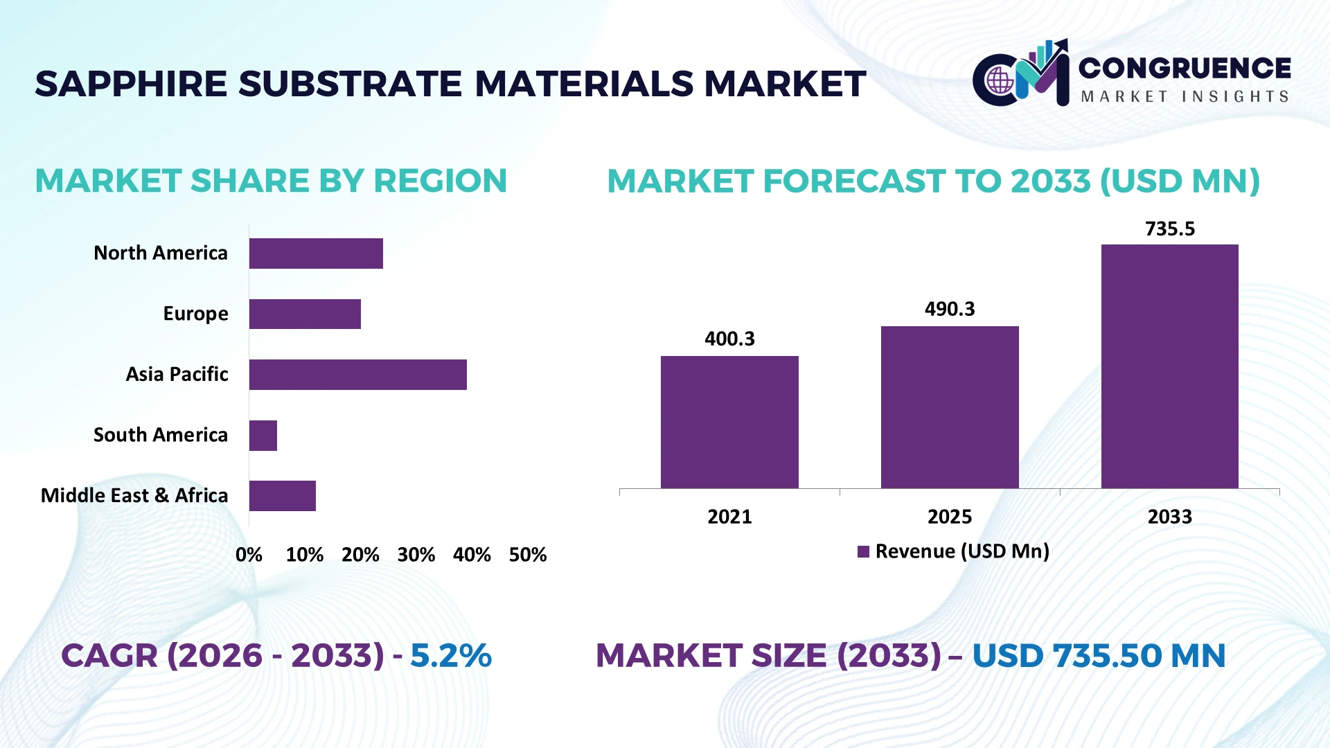
The Global Sapphire Substrate Materials Market was valued at USD 490.3 Million in 2025 and is anticipated to reach a value of USD 735.5 Million by 2033 expanding at a CAGR of 5.2% between 2026 and 2033. Growth is being driven by GaN-on-sapphire LED production, Mini-LED and Micro-LED scaling, larger-diameter wafer migration, and higher sapphire utilization in RF, photonics, automotive lighting, and high-reliability optoelectronics.
China remains the production center, absorbing roughly 55% of global sapphire wafer output, while sapphire represented 55.63% of China’s LED epitaxial substrate mix in 2025. More than 150 new MOCVD reactors were commissioned by Chinese LED manufacturers during 2024–2025, strengthening 6-inch and 8-inch substrate consumption. Taiwan remains comparatively concentrated in premium Mini-LED applications, while U.S. semiconductor localization under the CHIPS framework reinforces supply-chain diversification.
Strategically, suppliers controlling large-diameter crystal growth, precision polishing, patterned sapphire processing, and Asian customer qualification gain the strongest pricing and volume leverage as advanced-display manufacturing scales.
Market Size & Growth: USD 490.3 million in 2025 reaches USD 735.5 million by 2033 at 5.2% CAGR, supported by Mini-LED, Micro-LED and GaN device manufacturing.
Top Growth Drivers: Sapphire holds 55.67% of Asia-Pacific LED epitaxial substrate demand, while displays/backlighting and 200-mm-plus wafer formats are advancing at 15.62% and 13.16%, respectively.
Short-Term Forecast: By 2028, wider 6-inch and 8-inch processing will target lower cost per die; 12-inch sapphire formats provide approximately 2.3× the chip area of 8-inch wafers.
Emerging Technologies: AI-controlled crystal growth, automated thermal-field management and patterned sapphire substrates are accelerating; advanced patterning can improve LED light-extraction efficiency by nearly 33%.
Regional Leaders: Applying the current 47%/24%/20% regional structure to the 2033 outlook indicates approximately USD 346 million for Asia-Pacific, USD 177 million for North America and USD 147 million for Europe.
Consumer/End-User Trends: Sapphire accounted for 55.63% of China’s LED epitaxial substrate mix, reflecting continued qualification in automotive headlamps, outdoor lighting and high-reliability GaN devices.
Pilot/Case Example: In 2026, Jingsheng Electromechanical demonstrated 1,000-kg-class Kyropoulos sapphire growth after progressing from 300-kg, 450-kg and 750-kg crystals, materially increasing boule-scale production capability.
Competitive Landscape: China absorbs about 55% of global wafer output; major competitive participants include Kyocera, Crystal Applied Technology, Rubicon Technology, Monocrystal and Sumitomo Chemical.
Regulatory & ESG Impact: U.S. semiconductor localization remains strategically relevant, with CHIPS incentives totaling USD 30.9 billion across 40 semiconductor projects by July 2025, reinforcing diversified advanced-material sourcing.
Investment & Funding: Chinese LED manufacturers commissioned more than 150 MOCVD reactors during 2024–2025, while a CNY 2.8 billion expansion targeted Mini-LED and Micro-LED manufacturing capacity.
Innovation & Future Outlook: Sapphire retains approximately 70.24% of LED epitaxial substrate-material usage, but larger silicon, GaN and SiC platforms intensify competition, pushing suppliers toward patterned, larger-diameter and ultra-low-defect substrates.
Sapphire substrate materials are increasingly concentrated in high-performance LED epitaxy, Mini-LED displays, Micro-LED architectures, RF electronics, laser diodes and advanced optical systems. Sapphire already represents about 56% of Asia-Pacific LED epitaxial substrate usage, while larger-diameter wafers, AI-controlled crystal growth and patterned surfaces are improving manufacturing economics. China-centered production scale and semiconductor supply-chain localization are now shaping sourcing strategies, setting up the market’s broader strategic discussion.
Sapphire substrates are becoming strategically important as LED, Mini-LED, Micro-LED, RF and power-device manufacturers prioritize thermally stable, electrically insulating and high-hardness wafer platforms. China accounts for more than half of global sapphire wafer production, making supply concentration increasingly relevant as the United States, Japan and Europe restructure semiconductor supply chains. The shift is encouraging manufacturers to qualify geographically diversified crystal-growth, slicing and polishing capacity.
Technology economics are also changing. Patterned sapphire substrates can improve LED light-extraction efficiency by roughly 20–30% compared with conventional planar sapphire, while migration from 4-inch toward 6-inch wafers increases usable device area per processing cycle by more than 100%. China leads production scale and MOCVD deployment, whereas Japan maintains strength in high-purity materials and precision processing. Through 2028, 6-inch substrates will gain further qualification across advanced LED production.
Operationally, manufacturers are deploying automated Kyropoulos crystal-growth systems with thermal-field monitoring to improve boule consistency and reduce defect-related losses. Suppliers are consequently investing in larger crystals, automated inspection, patterned-wafer processing and closer partnerships with epitaxy producers. Competitive advantage will increasingly depend on defect control, diameter scalability and qualification reliability rather than commodity wafer volume alone.
Mini-LED, automotive lighting and GaN epitaxy are strengthening sapphire substrate utilization because the material combines thermal stability, electrical insulation and established MOCVD compatibility. Sapphire represents approximately 56% of China’s LED epitaxial substrate mix, while advanced patterned substrates can improve light extraction by 20–30% over conventional planar surfaces. Migration from 4-inch to 6-inch wafers provides about 125% more surface area per wafer, improving production throughput. China’s continuing expansion of Mini-LED manufacturing is therefore translating directly into larger-diameter substrate requirements. Producers are responding by expanding crystal-growth furnaces, precision slicing and patterned sapphire substrate capacity. Strategically, substrate suppliers qualified simultaneously for larger diameters and tighter defect specifications capture greater value than vendors competing primarily through wafer volume.
Sapphire remains processing-intensive because its Mohs hardness of 9 requires diamond-based slicing, grinding and polishing, increasing equipment wear and production time compared with silicon. China represents more than 50% of global sapphire wafer output, creating sourcing concentration for downstream manufacturers seeking geographically balanced semiconductor supply chains. Material utilization also deteriorates during boule slicing and edge processing, with kerf and finishing losses commonly removing more than 20% of the starting crystal volume. These constraints directly pressure margins when customers demand tighter flatness, lower defect density and larger wafer diameters. Manufacturers are reducing exposure through multi-year supply agreements, localized finishing operations and dual sourcing from Japan and other qualified markets. Operationally, reducing kerf loss delivers greater near-term economics than simply increasing furnace capacity.
Large-diameter sapphire creates a high-value pathway as Micro-LED, advanced photonics and next-generation GaN manufacturing demand greater wafer-level productivity. Moving from 4-inch to 8-inch substrates provides approximately 300% more surface area, enabling substantially more devices per processing cycle when epitaxy equipment supports larger formats. Patterned surfaces can simultaneously deliver 20–30% higher light extraction than planar alternatives, strengthening their value in premium display architectures. China is scaling larger crystal boules, while Taiwan and South Korea remain important development centers for Mini-LED and Micro-LED integration. Suppliers are directing R&D toward 8-inch processing, laser slicing, automated defect inspection and reusable sapphire concepts. A less obvious opportunity lies in selling engineered surfaces rather than untreated wafers, shifting competition toward differentiated substrate functionality and higher customer switching costs.
Scaling sapphire substrates without sacrificing crystal uniformity remains a critical execution challenge. An 8-inch wafer has roughly 4 times the surface area of a 4-inch wafer, meaning localized bow, stress or defect problems affect substantially more potential devices per failed substrate. Meanwhile, Micro-LED architectures can incorporate millions of microscopic emitters, making epitaxial consistency and defect control increasingly unforgiving. Larger Kyropoulos-grown boules therefore require tighter thermal-gradient management, orientation control and downstream polishing accuracy. China’s rapid furnace scaling intensifies the need to maintain repeatable quality across production lines rather than merely maximizing boule weight. Producers must invest in AI-assisted thermal control, automated optical inspection, metrology and closer substrate-epitaxy process integration. Long-term competitiveness depends on converting diameter expansion into stable usable yield; capacity without repeatability creates limited operational advantage.
Wafer Diameter Migration Accelerates: Sapphire processing is moving from 100 mm toward 150 mm and 200 mm formats as LED and compound-semiconductor manufacturers seek greater die output per epitaxy cycle. A 150 mm wafer provides roughly 125% more surface area than 100 mm, while 200 mm delivers about 300% more. Producers are upgrading polishing, metrology and wafer-handling systems to capture these productivity gains.
Crystal Growth Becomes More Automated: Manufacturers are deploying automated thermal-field control, machine-vision inspection and closed-loop furnace monitoring to stabilize large sapphire boules. Kyropoulos-grown crystals now exceed 1,000 kg in demonstrated Chinese production, versus approximately 300–450 kg in earlier commercial generations. Automation reduces operator-dependent variation and strengthens boule-to-boule consistency, pushing investment toward software-controlled furnaces and predictive process management.
Surface Specifications Become More Demanding: Mini-LED, high-brightness LED and precision optoelectronics are tightening requirements for total-thickness variation, wafer bow and surface roughness. Patterned surfaces can raise LED light extraction by approximately 20–30%, while semiconductor-grade polishing increasingly targets sub-nanometer roughness. Suppliers are adding precision CMP, automated defect mapping and application-specific surface treatments, shifting competition from basic wafer availability toward reproducible epitaxy-ready quality.
Substrate Competition Reshapes Positioning: GaN device manufacturers increasingly evaluate sapphire against silicon and SiC according to diameter, thermal performance and fabrication economics. Silicon platforms are progressing from 200 mm toward 300 mm, while native GaN generally remains limited to 150 mm. Sapphire suppliers are responding through specialized orientations, RF-grade material and Micro-LED integration rather than competing directly in every power-device architecture, creating defensible application-specific positions.
Sapphire Wafers lead the type segmentation with an estimated 35% share, reflecting their standardized integration across GaN epitaxy, LED fabrication, optical devices and specialty semiconductor processing. Their established availability from 100 mm through 150 mm formats supports high-volume MOCVD workflows. Polished Sapphire maintains strong demand where surface roughness, flatness and optical transmission directly affect device yield, while Single-Crystal Sapphire remains strategically important for high-purity optical, RF and high-temperature electronic applications.
Patterned Sapphire represents the fastest-expanding type as manufacturers pursue higher photon extraction and improved GaN epitaxial quality. Engineered surface patterns can improve LED light extraction by approximately 20–30% compared with planar substrates. Epitaxial Sapphire addresses customers seeking tighter orientation and deposition-ready specifications. Suppliers are consequently directing capital toward nano-patterning, chemical-mechanical polishing, automated inspection and larger wafer formats. Investment is moving away from undifferentiated substrate volume toward engineered wafers carrying higher qualification barriers and stronger customer retention.
LED Manufacturing accounts for an estimated 50% of sapphire substrate consumption, supported by established GaN-on-sapphire epitaxy across general lighting, automotive illumination, display backlighting and high-brightness emitters. Sapphire’s electrical insulation, thermal stability and compatibility with mature MOCVD infrastructure preserve its production advantage. Optical Components form a stable secondary application, particularly for high-hardness windows, sensors and laser assemblies requiring optical transparency and environmental resistance.
Semiconductor Devices represent the fastest-growing application as GaN-on-sapphire moves further into high-frequency electronics and specialized transistor architectures. RF Electronics is becoming strategically important for millimeter-wave systems, while Power Electronics remains more selective because SiC and silicon compete strongly where thermal conductivity or large-diameter economics dominate. Manufacturers are responding with lower-defect wafers, specialized crystal orientations and tighter surface specifications. The operational shift is important: sapphire demand is becoming less dependent on conventional lighting and increasingly linked to device architectures where substrate quality directly determines RF performance, epitaxial uniformity and manufacturing yield.
LED Manufacturers represent the leading end-user group with an estimated 46% share because high-volume GaN epitaxy requires continuous sapphire wafer procurement across lighting, automotive, Mini-LED and specialty emitter production. Their purchasing behavior increasingly favors larger diameters, controlled miscut angles and tighter surface tolerances. Electronics Manufacturers and Optoelectronics Companies form the next important customer base, using sapphire in displays, sensors, laser systems and high-durability optical assemblies.
Semiconductor Foundries are the fastest-expanding end-user group as compound-semiconductor workflows broaden into RF, photonics and specialized GaN devices. Research Institutions remain smaller-volume purchasers but exert disproportionate influence by validating non-polar GaN, Micro-LED transfer and alternative epitaxial architectures before commercial qualification. Suppliers are responding through joint development, customized wafer orientation, engineering samples and longer qualification partnerships. Future procurement is therefore shifting from transactional wafer purchasing toward process-specific collaboration, allowing suppliers with advanced metrology and application engineering to secure deeper positions inside customer fabrication workflows.
Asia-Pacific accounted for the largest market share at approximately 47% in 2025 however, Asia-Pacific is expected to register the fastest growth, expanding at a CAGR of approximately 6.2% between 2026 and 2033.

Defense, RF and Advanced Optics Drive Specialization
North America accounted for approximately 22% of global demand in 2025, with consumption concentrated across defense electro-optics, semiconductor equipment, RF electronics, aerospace sensors and high-performance optical systems. The market differs from Asian volume manufacturing because suppliers emphasize high-purity single-crystal sapphire, customized orientations, ultra-thin wafers and large optical components. U.S. semiconductor localization is also strengthening interest in domestically controlled advanced-material supply chains. Commercial capabilities now extend to sapphire parts approximately 200 microns thick, while large-area material is deployed in aircraft, UAV and infrared sensor windows. Suppliers are prioritizing vertically integrated crystal growth, grinding, polishing and precision fabrication to shorten qualification cycles. The strategic advantage lies in specification control and secure supply rather than commodity LED-wafer scale, supporting premium applications where material failure carries disproportionately high operational costs.
United States Market Outlook: The United States leads North American activity through established defense, aerospace, RF and semiconductor-equipment ecosystems. Domestic suppliers support applications ranging from electronics substrates to electro-optical windows, while government-backed programs have previously advanced sapphire window manufacturing toward 36 × 18-inch formats. ITAR-compliant production capabilities further strengthen domestic sourcing relevance for sensitive optical and defense programs.
GaN Research Moves Toward Production Scale
Europe represented approximately 17% of global sapphire substrate demand in 2025, with Germany, France and the United Kingdom supporting specialized consumption across compound semiconductors, photonics, industrial lasers and precision optics. Germany is particularly important as GaN development moves from laboratory-scale substrates toward manufacturing-compatible wafer formats. In 2025, researchers demonstrated N-polar GaN/AlGaN HFET structures grown using production-type MOCVD equipment on 200 mm sapphire, compared with earlier N-polar work largely limited to substrates up to 100 mm. This 4-fold increase in wafer surface area creates a clearer route toward scalable high-frequency device processing. European equipment and materials companies are consequently strengthening collaborations with universities and semiconductor laboratories. The market’s competitive position increasingly rests on process intellectual property, precision epitaxy and specialty device integration rather than high-volume sapphire crystal production.
Germany Market Outlook: Germany combines compound-semiconductor equipment expertise with advanced GaN research infrastructure. RWTH Aachen and AIXTRON demonstrated N-polar HFET processing on 200 mm sapphire, achieving electron mobility up to approximately 1,000 cm²/V·s and transit frequencies reaching 9 GHz. This positions Germany strongly for sapphire-supported RF and next-generation GaN process development.
Manufacturing Scale Shifts Toward Larger Boules
Asia-Pacific controlled approximately 47% of the global market in 2025, supported by China’s sapphire crystal production, Japan’s precision substrate processing, Taiwan’s optoelectronics ecosystem and South Korea’s advanced display manufacturing. China provides the strongest scale advantage as vertically integrated manufacturers combine crystal-growth furnaces with cutting, grinding and polishing operations. Large-boule development has progressed rapidly: Chinese producers have advanced from approximately 300 kg sapphire crystals to 450 kg, 750 kg and, by 2026, 1,000 kg-class Kyropoulos-grown material. Larger boules increase flexibility for wafer and optical-component fabrication while improving production economics when downstream yields remain controlled. Japanese suppliers complement this scale with LED-grade substrates reaching 150–200 mm specifications. Companies are increasingly integrating upstream crystal growth with downstream finishing, creating tighter control over quality, throughput and customer qualification.
China Market Outlook: China is the region’s principal manufacturing center, supported by vertically integrated equipment and advanced-material producers in industrial hubs including Zhejiang. Jingsheng Electromechanical demonstrated 1,000 kg-class synthetic sapphire in 2026 after progressing through multiple smaller boule generations. Its integration of crystal growth with cutting, grinding and polishing illustrates China’s shift from capacity expansion toward end-to-end sapphire processing control.
Import-Led Demand Follows Electronics Modernization
South America represented approximately 6% of global sapphire substrate demand in 2025, with Brazil carrying the strongest commercial relevance through electronics assembly, telecommunications, aerospace and optical-instrument applications. Regional consumption remains primarily import-dependent because local large-scale sapphire crystal-growth and semiconductor-grade wafer-processing infrastructure is limited. Demand therefore concentrates on finished wafers, optical windows, sensor components and specialty substrates rather than upstream boule production. Brazil’s established semiconductor and electronics policy framework is encouraging greater localization of advanced electronics, while telecommunications modernization supports RF and optoelectronic component requirements. Sapphire suppliers are addressing the market through distributors, application-specific imports and partnerships with local electronics manufacturers rather than capital-intensive crystal-growth installations. The main constraint remains qualification lead time and imported-material exposure, making inventory positioning and dependable technical support more commercially important than manufacturing scale within the region.
Brazil Market Outlook: Brazil offers the strongest South American demand base through its semiconductor, aerospace, telecommunications and industrial-electronics sectors. The country’s 2024 semiconductor-support framework extended incentives through 2029, strengthening local electronics manufacturing conditions. Sapphire suppliers benefit indirectly as higher-value RF, sensor, optical and compound-semiconductor applications require increasingly specialized substrate and component inputs.
Semiconductor Investment Creates New Demand Nodes
Middle East & Africa accounted for approximately 8% of global demand in 2025, with activity increasingly concentrated in the UAE, Saudi Arabia, Israel and selected South African technology clusters. Sapphire consumption remains specialized, spanning defense optics, photonics, RF electronics, aerospace systems and research applications. The structural shift comes from semiconductor and advanced-manufacturing investment rather than conventional LED substrate production. Saudi Arabia and the UAE are building technology ecosystems around localization, while Israel maintains established compound-semiconductor, electro-optics and defense capabilities. These markets favor high-specification wafers and optical sapphire that can meet demanding thermal, mechanical and purity requirements. Suppliers are positioning through technical partnerships, university collaborations and specialized distribution rather than local mass-production facilities. Winning projects increasingly requires application engineering and qualification support because emerging fabrication ecosystems lack Asia’s dense substrate-processing supply chain.
Saudi Arabia Market Outlook: Saudi Arabia is developing the strongest new investment-driven opportunity through its semiconductor localization agenda and National Semiconductor Hub. The initiative targets the development of 50 semiconductor design companies by 2030, creating an ecosystem for advanced electronics, photonics and related materials. Sapphire suppliers can position early through research partnerships, technical qualification and specialty substrate distribution.
Global specialists Kyocera, Rubicon Technology, Monocrystal, Crystalwise and Chinese integrated sapphire producers compete through crystal quality, wafer diameter, processing precision and supply control. The top five suppliers hold an estimated 45% combined share, leaving substantial volume with Chinese and Taiwanese regional manufacturers. Japanese suppliers emphasize reliability and precision, while Chinese producers increasingly compete through vertically integrated crystal growth and downstream finishing. Moving from 100 mm to 150 mm wafers increases processing area by 125%, making large-diameter capability a decisive productivity differentiator. Patterned surfaces can improve LED light extraction by 20–30%, shifting competition toward engineered substrates rather than polished commodity wafers. Players are expanding larger-boule growth, automated polishing, metrology and customer-specific qualification partnerships. The current shift favors suppliers controlling both crystal growth and finishing as customers tighten defect and traceability requirements. Capital-intensive furnaces, lengthy epitaxy qualification and yield consistency remain strong entry barriers. Winning requires scalable diameter, reproducible quality, application engineering and dependable supply.
Kyocera Corporation
Rubicon Technology
Monocrystal
Crystalwise Technology
Namiki Precision Jewel
CrysTec GmbH
Zhejiang Jingsheng Mechanical & Electrical
Zhejiang Crystal-Optech
Jiangsu Jeshine New Material
Phecda Technology
Tera Xtal Technology
Panyu Jingcheng OnOpto-Electronic Material
Sichuan Tianyou Optoelectronics
Advanced Crystal Technology
Current sapphire manufacturing is shifting toward larger Kyropoulos boules, automated metrology, and 150–200 mm wafers. Moving from 100 mm to 150 mm increases usable wafer area by 125%, raising epitaxy throughput without proportionally increasing reactor cycles. Advanced polishing achieving sub-nanometer surface roughness reduces nucleation variability, while automated optical inspection improves defect-screening efficiency by roughly 15–20%. Adoption is strongest among LED, RF, photonics, and semiconductor producers requiring tighter wafer geometry and repeatable epitaxial performance.
Emerging technology centers on patterned sapphire substrates, AI-assisted thermal-field control, laser slicing, and ultra-clean surface preparation. Patterned surfaces can improve LED light extraction by 20–30% versus conventional planar sapphire, while optimized nanoimprint workflows can raise patterning-line throughput by 30%. Large-diameter N-polar GaN processing on 200 mm sapphire demonstrates integration with production-type MOCVD, extending sapphire beyond mature lighting applications. Vertically integrated growers benefit through lower handling losses, faster qualification, and stronger process control.
Disruptive commercial development through 2026–2028 will focus on 12-inch substrates, one-ton-class crystals, intelligent furnaces, and engineered sapphire for Micro-LED, quantum, and high-frequency devices. Compared with 100 mm wafers, 200 mm formats provide 300% more area, improving device density per run. Suppliers investing now gain differentiation through diameter scalability, defect control, specialized orientations, and application-specific surfaces.
September 2024 Kyocera introduced high-crystallinity sapphire wafers for quantum systems at Quantum Effects 2024, targeting lower dielectric loss and thermal conductivity above 100 W/mK at cryogenic temperatures, expanding sapphire positioning from established electronics substrates into quantum-computing hardware applications. Source: kyocera.com
February 2025 Janel disclosed its 46.6% ownership of Rubicon Technology, a monocrystalline sapphire specialist, alongside board representation supporting restructuring and profitability initiatives, strengthening strategic oversight of a U.S. supplier serving high-performance precision advanced optical and industrial sapphire applications. Source: sec.gov
October 2025 AIXTRON and RWTH Aachen demonstrated N-polar GaN/AlGaN HFETs grown on 200-mm sapphire using production-type MOCVD, achieving mobility up to 1,000 cm²/V·s and 9-GHz transit frequency, materially advancing cost-efficient industrial-scale sapphire-based manufacturing for high-frequency commercial semiconductor devices. Source: aip.org
August 2026 Jingsheng Electromechanical confirmed scaled production of 1,000-kg-class Kyropoulos sapphire crystals and 4–8-inch substrates, alongside development up to 12 inches, strengthening vertical integration across crystal growth, cutting, grinding and polishing while reducing material losses in large-format manufacturing. Source: chinadaily.com
The Sapphire Substrate Materials Market report evaluates Polished Sapphire, Epitaxial Sapphire, Patterned Sapphire, Single-Crystal Sapphire and Sapphire Wafers across LED Manufacturing, Semiconductor Devices, RF Electronics, Optical Components and Power Electronics. Coverage extends to LED manufacturers, semiconductor foundries, electronics manufacturers, optoelectronics companies and research institutions, with analysis spanning North America, Europe, Asia-Pacific, South America and Middle East & Africa.
The scope examines 100–200 mm wafer migration, 12-inch development, patterned surfaces delivering approximately 20–30% higher LED light extraction, automated crystal growth, precision polishing and one-ton-class sapphire boules. It also assesses Micro-LED, quantum computing, GaN RF devices and specialty optical applications. Between 2026 and 2033, the analysis supports investment planning, manufacturing expansion, supplier qualification, technology positioning and competitive strategy by identifying where larger formats, engineered surfaces, vertical integration and application-specific substrate specifications are reshaping commercial priorities.
| Report Attribute/Metric | Report Details |
|---|---|
Market Revenue in 2025 | USD 490.3 Million |
Market Revenue in 2033 | USD 735.5 Million |
CAGR (2026 - 2033) | 5.2% |
Base Year | 2025 |
Forecast Period | 2026 - 2033 |
Historic Period | 2021 - 2025 |
Segments Covered | By Type
By Application
By End-User
|
Key Report Deliverable | Revenue Forecast, Growth Trends, Market Dynamics, Segmental Overview, Regional and Country-wise Analysis, Competition Landscape |
Region Covered | North America, Europe, Asia-Pacific, South America, Middle East, Africa |
Key Players Analyzed | Kyocera Corporation, Rubicon Technology, Monocrystal, Crystalwise Technology, Namiki Precision Jewel, CrysTec GmbH, Zhejiang Jingsheng Mechanical & Electrical, Zhejiang Crystal-Optech, Jiangsu Jeshine New Material, Phecda Technology, Tera Xtal Technology, Panyu Jingcheng OnOpto-Electronic Material, Sichuan Tianyou Optoelectronics, Advanced Crystal Technology |
Customization & Pricing | Available on Request (10% Customization is Free) |