
Reports
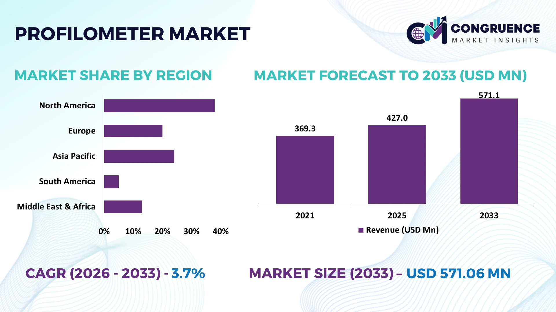
The Global Profilometer Market was valued at USD 427.02 Million in 2025 and is anticipated to reach a value of USD 571.06 Million by 2033 expanding at a CAGR of 3.7% between 2026 and 2033. Growth is driven by semiconductor fabrication localization, tighter nanometer surface metrology requirements, and automated three dimensional inspection across wafers, precision optics, advanced coatings, automotive components, and additive manufacturing.
The United States represents the dominant country market, supported by semiconductor fabrication, aerospace, precision optics, medical devices, and nanotechnology. Federal semiconductor programs provide USD 52.7 billion for manufacturing, research, and workforce development, while domestic chipmaking capacity is projected to increase 203% between 2022 and 2032. By comparison, global capacity is projected to rise 86%. Intensifying United States and China semiconductor competition is accelerating localized fabrication and process control investment, strengthening demand for automated optical and nanometer scale profilometry.
Profilometer manufacturers combining subnanometer measurement, automated three dimensional inspection, semiconductor process integration, and high throughput analytics are positioned strongest as advanced manufacturing shifts toward tighter surface control.
Market Size & Growth: USD 427.02 million in 2025 advances to USD 571.06 million by 2033 at 3.7% CAGR, supported by semiconductor localization, automated inspection, and increasingly stringent surface metrology.
Top Growth Drivers: Semiconductor localization is supported by a projected 203% increase in United States chipmaking capacity, advanced logic manufacturing capacity is positioned to reach 28% of global capacity, and domestic semiconductor capital investment exceeds USD 500 billion.
Short Term Forecast: By 2028, automated optical profiling workflows can reduce measurement cycle time by more than 30% compared with sequential contact based inspection, strengthening throughput in high volume precision manufacturing.
Emerging Technologies: AI assisted defect classification, confocal microscopy, and white light interferometry are advancing automated three dimensional metrology, with premium optical systems achieving vertical resolution below 1 nanometer.
Regional Leaders: North America benefits from more than USD 500 billion in announced semiconductor investment, Asia Pacific leads fabrication scale, and Europe is targeting 20% of global semiconductor production under its semiconductor industrial strategy.
Consumer/End User Trends: Semiconductor manufacturers are shifting toward 100% inspection at selected critical process stages, replacing sample based measurement where nanoscale surface defects directly affect wafer yield and device reliability.
Pilot/Case Example: Advanced optical profilometry systems operating in 2025 delivered subnanometer vertical resolution while capturing millions of three dimensional surface points, reducing dependence on slower sequential stylus measurements.
Competitive Landscape: Keyence competes with Bruker, KLA, Zygo, and Taylor Hobson, with advanced platforms increasingly differentiated by nanometer resolution, automated three dimensional analysis, measurement speed, and production integration.
Regulatory & ESG Impact: Noncontact optical profiling provides 100% contact free surface measurement, eliminating stylus induced scratching on sensitive wafers, optical coatings, thin films, and precision engineered surfaces while reducing destructive inspection requirements.
Investment & Funding: More than USD 500 billion in announced United States semiconductor projects is expanding fabrication and packaging infrastructure, creating downstream requirements for automated surface characterization, process validation, and nanoscale quality control.
Innovation & Future Outlook: Next generation profilometers combine AI analytics, automated three dimensional mapping, and subnanometer vertical resolution, moving surface metrology from offline laboratory inspection toward integrated manufacturing process control.
The Profilometer Market is becoming increasingly important across semiconductor fabrication, precision optics, thin film coatings, automotive components, additive manufacturing, microelectronics, and advanced materials. Optical profilometers are gaining adoption because noncontact measurement eliminates mechanical interaction with 100% of inspected surfaces while supporting rapid three dimensional characterization. White light interferometry, confocal imaging, automated stage control, and AI assisted defect analysis are extending profilometry from laboratory verification into production environments. Semiconductor supply chain localization across the United States, Japan, Europe, and China is simultaneously increasing process metrology intensity, establishing measurement repeatability, automation, throughput, and manufacturing integration as the next strategic priorities.
Profilometers are becoming strategically important as semiconductor, precision optics, medical device, automotive, and advanced coating manufacturers tighten surface control from micrometer inspection toward nanometer scale process verification. United States semiconductor manufacturing capacity is projected to rise 203% between 2022 and 2032, intensifying domestic metrology requirements as fabrication supply chains localize. Profilometry therefore increasingly influences yield control, qualification speed, and manufacturing competitiveness rather than serving only laboratory inspection.
Optical profilometers provide a decisive operational advantage over legacy stylus instruments by capturing millions of three dimensional surface points without contacting the component. Automated optical workflows can reduce measurement cycles by more than 30%, while premium interferometric platforms achieve vertical resolution below 1 nanometer. Asia Pacific leads semiconductor production scale, whereas the United States is accelerating advanced fabrication investment and Europe emphasizes precision industrial and semiconductor capacity.
Through 2028, inline optical measurement, AI assisted defect classification, and automated three dimensional analysis will gain importance. Semiconductor fabs deploying profilometers beside process equipment can identify roughness or step height deviations before downstream processing. Vendors are consequently investing in automation, software integration, and application partnerships. Competitive advantage will increasingly depend on converting high resolution surface data into faster production decisions.
Semiconductor manufacturing is the strongest structural driver as smaller geometries, advanced packaging, and localized fabrication increase surface measurement frequency. United States chip manufacturing capacity is projected to expand 203% between 2022 and 2032, versus 86% globally, while the country is positioned to capture 28% of advanced logic capacity below 10 nanometers. These shifts increase requirements for step height, roughness, film thickness, and wafer topography control. Government backed fabrication localization following semiconductor supply disruptions has made metrology capacity strategically important rather than optional laboratory infrastructure. Profilometer manufacturers are responding with automated wafer stages, noncontact optical platforms, and software integrated inspection. The operational advantage lies in detecting surface deviations before expensive downstream processing, protecting yield as fabrication complexity rises.
High specification optical profilometers remain difficult to scale across cost sensitive factories because nanometer resolution requires precision optics, vibration isolation, controlled environments, calibration infrastructure, and specialized software. Optical systems can cost several times more than basic stylus instruments, while advanced semiconductor facilities require temperature stability near ±1°C and vibration management for repeatable nanoscale measurement. Smaller manufacturers therefore retain contact instruments where surface geometry and throughput requirements permit. Export controls affecting advanced semiconductor equipment between the United States and China also complicate technology access and service planning for globally distributed operations. Vendors are reducing exposure through modular platforms, localized technical support, longer service agreements, and multiple measurement configurations. Lower acquisition cost alone is insufficient because calibration continuity and measurement traceability increasingly determine lifetime operating economics.
The strongest opportunity lies in moving profilometry from offline laboratories directly into automated manufacturing workflows. Optical systems can inspect surfaces without physical contact, eliminating measurement induced damage on 100% of inspected wafers, coatings, and delicate microstructures. Advanced platforms deliver vertical resolution below 1 nanometer, while automated measurement can shorten inspection cycles by more than 30% compared with sequential stylus workflows. Japan, the United States, and Taiwan are expanding advanced semiconductor and packaging capacity, creating opportunities for integrated wafer topography and process control systems. AI based defect classification adds another layer by converting three dimensional datasets into actionable production decisions. Manufacturers are investing in automated stages, robotic handling, analytics software, and equipment partnerships. The non obvious opportunity is recurring software and application engineering value beyond instrument sales.
The long term challenge is integrating high resolution profilometry into production environments without creating data, workflow, and skills bottlenecks. Three dimensional optical systems can generate millions of measurement points per scan, making automated analysis essential when factories move toward 100% inspection at critical stages. Semiconductor manufacturers simultaneously face a workforce constraint as United States industry expansion is projected to leave 67,000 technical positions unfilled by 2030. Measurement inconsistency across stylus, confocal, interferometric, and focus variation platforms further complicates cross factory process control because different technologies can produce different roughness results on identical surfaces. Suppliers must therefore invest in standardized analytics, automated calibration, interoperable manufacturing software, and operator training. Competitive durability will depend on making nanometer measurement reproducible across tools, factories, materials, and production shifts.
Optical Platforms Replace Contact Workflows: Manufacturers are shifting delicate surface inspection toward noncontact profilometry, eliminating stylus interaction across 100% of measured areas. Advanced white light systems achieve vertical resolution below 1 nanometer and can reduce measurement cycles by over 30%. Semiconductor and precision optics companies are expanding automated optical inspection to protect sensitive coatings, accelerate measurement, and reduce operator dependent variability.
Hybrid Metrology Gains Production Relevance: Profilometer vendors are combining confocal, interferometric, and focus based measurement to handle surfaces that single sensor systems cannot characterize consistently. Modern platforms can capture millions of three dimensional points per scan and measure features from nanometer roughness to millimeter scale geometry. Companies are integrating interchangeable sensors and automated analysis, reducing equipment duplication while expanding measurement coverage across mixed production environments.
Advanced Packaging Reshapes Inspection: Chiplet integration and three dimensional packaging are increasing demand for bump height, coplanarity, warpage, and microstructure measurement. United States advanced logic capacity below 10 nanometers is positioned to reach 28% of global capacity, while domestic fabrication capacity is projected to rise 203%. Metrology suppliers are adapting platforms for automated wafer handling and larger three dimensional datasets as semiconductor supply chains localize.
AI Accelerates Surface Interpretation: Artificial intelligence is shifting profilometry from measurement collection toward automated defect interpretation. Production platforms increasingly classify millions of surface points while 100% inspection becomes practical at selected critical stages. With the United States semiconductor workforce facing a projected 67,000 worker gap by 2030, suppliers are expanding recipe automation, machine vision analytics, and standardized reporting to reduce specialist intervention and accelerate production decisions.
Optical systems represent the leading type with an estimated 45% market share, supported by noncontact operation, rapid three dimensional acquisition, and suitability for semiconductor wafers, coatings, optics, and sensitive microstructures. White Light systems strengthen this position by providing subnanometer vertical resolution on suitable surfaces. Contact systems remain relevant for established industrial quality control, while Stylus instruments retain demand where straightforward roughness measurement, traceability, and lower equipment cost outweigh throughput requirements.
Confocal is the fastest advancing type as manufacturers require three dimensional characterization of steep slopes, complex textures, and surfaces difficult to measure through conventional interferometry. Laser Scanning systems complement this shift where larger measurement ranges and rapid topographic mapping are required. Optical measurement can reduce inspection cycles by more than 30%, while eliminating physical contact across 100% of the measured surface. Vendors are consequently prioritizing multisensor integration, automated stages, advanced analysis software, and application specific configurations, shifting investment toward flexible platforms capable of replacing several standalone measurement workflows.
Surface Roughness represents the leading application with an estimated 35% market share because finish specifications directly influence friction, adhesion, sealing, fatigue behavior, optical performance, and component qualification. Surface Profiling remains important across precision manufacturing, while Step Height Measurement supports semiconductor patterning and microfabrication. Modern optical platforms provide vertical resolution below 1 nanometer, extending roughness analysis from conventional machined components into thin films, wafers, and nanoscale engineered surfaces.
Wafer Inspection is the fastest advancing application as semiconductor manufacturers increase metrology intensity across advanced logic, packaging, and three dimensional integration. Thin Film Measurement is becoming more closely integrated with process control, while Microstructure Analysis benefits from high density three dimensional datasets. United States semiconductor manufacturing capacity is projected to increase 203% between 2022 and 2032, strengthening requirements for wafer topography and process verification. Profilometer suppliers are responding with automated wafer stages, faster scanning, recipe based inspection, and integrated analytics, positioning surface measurement closer to production rather than centralized laboratories.
Semiconductor manufacturers represent the leading end user group with an estimated 35% market share, reflecting intensive measurement of wafers, thin films, patterned structures, packaging features, and surface defects. Electronics manufacturers provide another substantial demand base, while Automotive and Precision Engineering users emphasize roughness, wear, dimensional integrity, and production quality. Semiconductor requirements increasingly extend below 10 nanometers, pushing purchasing decisions toward automated optical systems with subnanometer vertical resolution and integrated three dimensional analytics.
Medical Devices represent the fastest advancing end user segment as surface texture becomes increasingly important for implants, microfluidics, surgical components, and precision manufactured devices. Aerospace customers require traceable measurement of coatings and critical components, while Research Institutes support adoption of advanced confocal, White Light, and Laser Scanning platforms. United States advanced logic manufacturing capacity is positioned to reach 28% of global capacity by 2032. Vendors are therefore developing semiconductor specific automation, customized medical measurement workflows, service partnerships, and modular platforms addressing different production economics.
North America accounted for the largest market share at 34% in 2025 however, Asia Pacific is expected to register the fastest growth, expanding at a CAGR of 6.7% between 2026 and 2033.

Advanced Manufacturing Drives Precision Metrology
North America held about 34% of the Profilometer Market in 2025, supported by semiconductor fabrication, aerospace engineering, medical devices, automotive manufacturing, and nanotechnology research. The United States concentrates regional demand as new fabs require surface roughness, wafer topography, thin film, and step height measurement across increasingly complex processes. Domestic semiconductor manufacturing capacity is projected to increase 203% between 2022 and 2032, while the US share of advanced logic production below 10 nanometers is positioned to reach 28%. Profilometer vendors are consequently expanding automated optical platforms, wafer handling capabilities, three dimensional measurement software, and local calibration support. Canada contributes aerospace and precision engineering demand, while Mexico's electronics and automotive manufacturing base supports production oriented inspection systems. This industrial mix favors suppliers combining nanometer measurement with automation and dependable lifecycle service.
United States Market Outlook: The United States is the regional technology and deployment center, with semiconductor, aerospace, biomedical, and precision engineering customers supporting premium profilometer adoption. More than USD 500 billion in announced semiconductor ecosystem investments is creating a broader installed base for wafer metrology. Vendors with automated inspection, certified calibration, and semiconductor process integration gain the strongest positioning as new fabrication capacity becomes operational.
Quality Compliance Sustains Advanced Metrology
Europe represented about 28% of the Profilometer Market in 2025, with Germany, France, the United Kingdom, and Italy supporting demand through automotive engineering, aerospace manufacturing, semiconductor development, medical devices, and precision machining. European procurement places substantial emphasis on measurement traceability, surface standards, and repeatable quality verification, supporting both stylus and advanced optical platforms. The European Chips Act targets mobilization of more than EUR 43 billion in public and private investment, expanding the semiconductor infrastructure requiring wafer and thin film metrology. Automotive electrification adds another measurement layer as battery components, power electronics, coatings, and precision drivetrain surfaces require controlled texture. Suppliers are responding through application laboratories, multisensor platforms, automated analysis, and stronger calibration networks. Europe therefore remains attractive for manufacturers competing through measurement integrity and specialized application engineering rather than equipment volume alone.
Germany Market Outlook: Germany combines semiconductor expansion with one of Europe's strongest automotive, optics, machinery, and precision engineering ecosystems. Major semiconductor projects are expanding fabrication infrastructure while automotive manufacturers intensify surface inspection for electrified powertrains and advanced components. This creates demand for high resolution optical systems alongside established traceable contact measurement, favoring suppliers with local application engineering and calibration capabilities.
Electronics Scale Accelerates Metrology Deployment
Asia Pacific accounts for about 30% of the global Profilometer Market, with China, Taiwan, South Korea, and Japan concentrating semiconductor, display, electronics, automotive, and precision component production. High manufacturing throughput makes measurement speed and automation particularly important, accelerating deployment of noncontact optical systems for wafer inspection, surface profiling, and microstructure analysis. China represented about 31% of Asia Pacific profilometer demand in 2025, while Taiwan and South Korea continue expanding advanced foundry and memory infrastructure. Japanese manufacturers add strength in precision instrumentation, optics, and industrial automation. Suppliers are scaling regional service, automated stages, production software, and application specific configurations to shorten inspection cycles. Dense electronics supply chains also create an important competitive advantage: profilometer vendors can validate new systems directly within high volume production environments and accelerate subsequent commercial deployment.
China Market Outlook: China combines extensive electronics production with semiconductor localization, EV manufacturing, display fabrication, and precision machinery demand. Government backed semiconductor programs are strengthening domestic equipment ecosystems while international suppliers retain advantages in advanced optical resolution and established process qualification. This competitive structure is pushing profilometer manufacturers toward localized support, faster automation, and application specific platforms designed for high volume factories.
Industrial Quality Control Broadens Adoption
South America represents roughly 6% of profilometer demand, with Brazil concentrating adoption across automotive production, aerospace manufacturing, metalworking, research laboratories, medical technology, and emerging semiconductor activity. Surface metrology remains more concentrated in established industrial clusters than in fully automated production networks, supporting a mix of stylus instruments and flexible optical systems. Brazil's semiconductor strategy gained structural support through the Brasil Semicon program, established under Law 14,968 and further regulated in 2026 to strengthen domestic production, research, and innovation. Argentina contributes specialized research and precision engineering demand, while other markets rely heavily on imported metrology equipment and distributor support. Vendors are therefore prioritizing service availability, operator training, modular equipment, and partnerships with local distributors rather than large direct infrastructure commitments. Reliable calibration coverage remains particularly important for expanding industrial adoption.
Brazil Market Outlook: Brazil provides the region's strongest opportunity through its aerospace, automotive, medical, machinery, and semiconductor ecosystem. Brasil Semicon expands policy support across chip production, research, and technological development, creating an additional pathway for precision measurement equipment. Profilometer suppliers that combine application training, accessible servicing, and flexible optical and contact configurations can address both advanced laboratories and industrial quality departments.
Technology Localization Creates New Metrology Demand
Middle East and Africa account for roughly 5% of Profilometer Market activity, with demand concentrated in energy equipment, aerospace, research laboratories, medical manufacturing, precision engineering, and emerging semiconductor initiatives. The UAE, Saudi Arabia, Israel, and South Africa provide the strongest advanced technology environments, although imported equipment continues to dominate surface metrology procurement. Saudi Arabia's National Semiconductor Hub is building a domestic ecosystem spanning semiconductor design, technology development, universities, research centers, international companies, and venture capital. Ten international semiconductor companies were expected to begin operations through the initiative during 2025, strengthening requirements for supporting characterization and quality infrastructure. Profilometer suppliers are addressing this developing market through distributor networks, research partnerships, technical training, and compact optical systems. Successful expansion depends heavily on dependable calibration, technical support, and integration expertise rather than equipment availability alone.
Saudi Arabia Market Outlook: Saudi Arabia is emerging as a strategically important technology market as semiconductor localization complements established aerospace, energy, research, and advanced manufacturing investment. The National Semiconductor Hub is designed to connect startups, universities, research centers, international companies, and investors across the semiconductor ecosystem. This infrastructure creates a new entry point for profilometer suppliers offering precision characterization, training, and locally supported metrology systems.
Bruker, KLA, KEYENCE, AMETEK Taylor Hobson, and Sensofar compete across optical, stylus, confocal, and semiconductor surface metrology, with premium technology suppliers facing specialists emphasizing application flexibility and price. The top five hold an estimated 46% combined share, indicating moderate concentration around measurement portfolios. Competition increasingly centers on subnanometer vertical resolution, where advanced optical platforms deliver over 30% faster inspection than sequential contact workflows, while noncontact systems eliminate stylus interaction across 100% of measured surfaces. Bruker and KLA emphasize semiconductor integration and automated analytics; KEYENCE competes through rapid deployment and usability; Taylor Hobson leverages traceable precision metrology; Sensofar advances multisensor optical configurations. Vendors are expanding software automation, application laboratories, partnerships, and vertically integrated measurement ecosystems. The competitive shift favors automated three dimensional analysis over standalone measurement hardware. Calibration expertise, optical engineering, software integration, and customer qualification remain entry barriers. Winning requires measurement accuracy, application depth, automation, service responsiveness, and scalable integration.
Bruker Corporation
KLA Corporation
KEYENCE Corporation
AMETEK
Sensofar
Mitutoyo Corporation
Nikon Corporation
Mahr
Alicona Imaging
Nanovea
Tokyo Seimitsu
Cyber Technologies
Polytec
Rtec Instruments
Current profilometry technology is shifting from contact stylus measurement toward automated optical platforms using white light interferometry, confocal imaging, and focus variation. Premium optical systems achieve vertical resolution below 1 nanometer while eliminating physical contact across 100% of inspected surfaces. Compared with sequential stylus workflows, automated three dimensional optical measurement can improve inspection speed by more than 30%, benefiting semiconductor, optics, and precision engineering manufacturers requiring surface qualification.
Emerging systems combine multisensor hardware with AI assisted defect classification, automated stages, and recipe driven analysis. Confocal platforms improve measurement coverage on steep slopes and microstructures, while interferometry provides subnanometer height sensitivity on surfaces. Automated analysis can reduce operator intervention by about 25%, supporting deployment across wafer inspection and advanced packaging. Vendors integrating measurement hardware, analytics, robotics, and manufacturing software gain advantage over standalone instrument suppliers.
Between 2026 and 2028, inline profilometry and adaptive measurement software will become important as factories expand process control. AI driven classification can shorten interpretation cycles by over 20%, while integrated handling improves equipment utilization by 15%. Semiconductor fabs and high volume electronics manufacturers benefit most because measurement data can trigger process corrections earlier. Suppliers investing in interoperability, automated calibration, and application specific software will secure integration.
September 2026 Sensofar launched S neox 6, integrating four optical technologies with enhanced automation, autofocus and automated leveling. The platform builds on 25 years of metrology development, enabling faster multi surface characterization and higher throughput across semiconductor and precision manufacturing.
November 2025 Evident launched the LEXT OLS5500 hybrid 3D optical profilometer, combining laser scanning, white light interferometry and focus variation. Its high NA WLI optics deliver up to 40 times faster throughput, strengthening production ready inspection across complex surfaces today.
July 2026 Cornell Center for Materials Research deployed KEYENCE VK X3000 3D optical profilometry, replacing two older systems. Demonstrated accuracy reached about 20 nm, with single digit nanometer capability under suitable noise conditions, expanding shared laboratory measurement precision and versatility.
October 2024 Taylor Hobson launched Form Talysurf PGI Optics PRO with fully automated routines for aspheric, diffractive and Fresnel surfaces. Supporting optical components up to 300 mm, the platform strengthens automated form measurement and production inspection for precision optics manufacturers.
The Profilometer Market Report evaluates Contact, Optical, Laser Scanning, Stylus, White Light, and Confocal technologies across Surface Roughness, Thin Film Measurement, Step Height Measurement, Wafer Inspection, Surface Profiling, and Microstructure Analysis. Coverage extends to Semiconductor, Electronics, Automotive, Aerospace, Medical Devices, Precision Engineering, and Research Institutes, with optical systems representing a leading technology segment as production shifts toward automated noncontact three dimensional measurement.
Regional assessment covers North America, Europe, Asia Pacific, South America, and Middle East and Africa, examining semiconductor fabrication, precision manufacturing, metrology infrastructure, automation, and equipment deployment. The report tracks subnanometer optical measurement, multisensor integration, AI assisted analysis, automated inspection, and niche advanced packaging applications. Competitive assessment of 14 influential participants supports investment planning, capacity expansion, partnership selection, technology positioning, and strategic market direction from 2026 through 2033.
| Report Attribute/Metric | Report Details |
|---|---|
Market Revenue in 2025 | USD 427.02 Million |
Market Revenue in 2033 | USD 571.06 Million |
CAGR (2026 - 2033) | 3.7% |
Base Year | 2025 |
Forecast Period | 2026 - 2033 |
Historic Period | 2021 - 2025 |
Segments Covered | By Type
By Application
By End-User
|
Key Report Deliverable | Revenue Forecast, Growth Trends, Market Dynamics, Segmental Overview, Regional and Country-wise Analysis, Competition Landscape |
Region Covered | North America, Europe, Asia-Pacific, South America, Middle East, Africa |
Key Players Analyzed |
|
Customization & Pricing | Available on Request (10% Customization is Free) |