
Reports
The Global Photonics Integrated Circuit Market was valued at USD 1373 Million in 2025 and is anticipated to reach a value of USD 1952.54 Million by 2033 expanding at a CAGR of 4.5% between 2026 and 2033. Growth is driven by AI data-center interconnects, silicon photonics, coherent optical communications, LiDAR, high-speed transceivers, and co-packaged optics requiring higher bandwidth density with lower electrical interconnect losses.
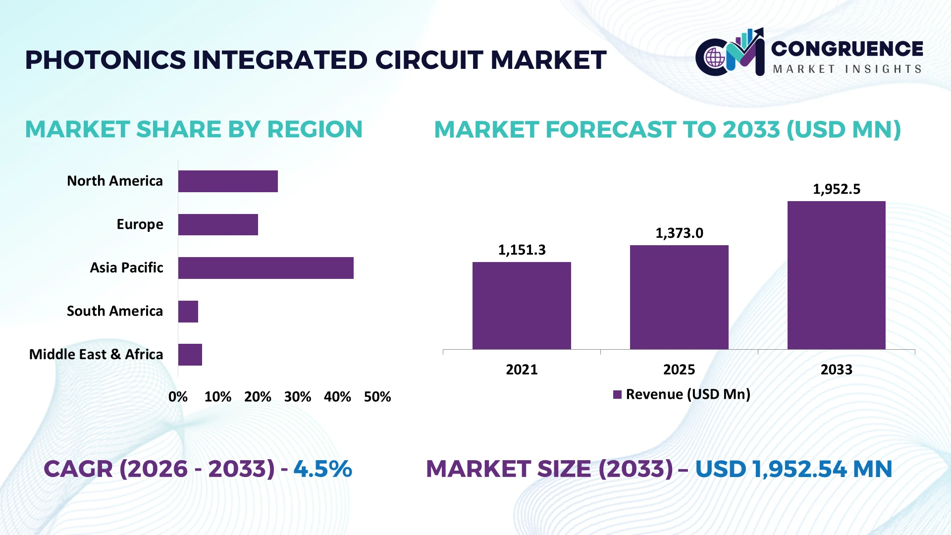
The United States accounts for an estimated 30–35% of global photonic integrated circuit demand, anchored by hyperscale AI infrastructure, semiconductor design, cloud networking, defense, and advanced sensing. Data-center migration from 400G toward 800G doubles nominal interface capacity by 100%, strengthening silicon-photonic integration. Taiwan offers greater semiconductor foundry and advanced-packaging scale, while the Netherlands leads critical photonics equipment capabilities. U.S.-China semiconductor restrictions are accelerating domestic photonics investment and diversified fabrication strategies, making foundry access and packaging capacity strategically important.
Strategically, suppliers combining photonic design, wafer-scale fabrication, lasers, advanced packaging, and high-volume testing gain the strongest position as integrated optics moves from specialized components into AI-scale infrastructure.
Market Size & Growth: USD 1,373 million in 2025 reaches USD 1,952.54 million by 2033 at 4.5% CAGR, driven by silicon-photonics deployment in high-speed AI connectivity.
Top Growth Drivers: AI interconnects contribute approximately 35%, telecom modernization 25%, and sensing/LiDAR applications 15% to incremental photonic-integration demand.
Short-Term Forecast: By 2028, advanced photonic integration is positioned to reduce optical-module power per transmitted bit by approximately 20–30% versus less-integrated architectures.
Emerging Technologies: Silicon photonics, thin-film lithium niobate, and co-packaged optics target 30–50% improvements in bandwidth density through tighter electronic-photonic integration.
Regional Leaders: By 2033, North America approaches USD 680 million, Asia-Pacific USD 625 million, and Europe USD 430 million as AI, telecom, and foundry deployments expand.
Consumer/End-User Trends: Data-center and telecommunications applications represent approximately 55–60% of PIC demand as 800G and emerging 1.6T interfaces increase integrated-photonics content.
Pilot/Case Example: In 2025, 1.6T silicon-photonic transceiver demonstrations delivered 100% higher nominal interface capacity than established 800G products, validating next-generation AI interconnect architectures.
Competitive Landscape: Intel maintains an estimated 15–20% position in silicon-photonics shipments, alongside Cisco, Broadcom, Coherent, and Lumentum across integrated optical connectivity.
Regulatory & ESG Impact: Integrated photonics can lower interconnect power requirements by approximately 20–30%, supporting data-center energy-efficiency targets as AI computing increases facility power density.
Investment & Funding: More than USD 500 million in recent public and private photonics initiatives is supporting fabrication, packaging, foundries, and commercialization across the United States and Europe.
Innovation & Future Outlook: Co-packaged optics and 1.6T connectivity target 2× the capacity of 800G interfaces, shifting investment toward wafer-scale photonics, integrated lasers, and automated packaging.
The Photonics Integrated Circuit Market is increasingly concentrated around AI data-center connectivity, coherent telecom systems, LiDAR, sensing, quantum technologies, and high-performance computing. Silicon photonics, integrated lasers, thin-film lithium niobate, and co-packaged optics are moving photonic functions onto smaller, denser platforms; 1.6T interfaces provide 100% greater nominal capacity than 800G designs. Semiconductor localization and U.S.-China technology restrictions are also elevating foundry access, advanced packaging, and supply-chain resilience as procurement priorities. This convergence of bandwidth, energy, manufacturing, and geopolitical requirements establishes the strategic context for future PIC investment and competitive positioning.
Photonic integrated circuits are becoming strategic semiconductor infrastructure as AI clusters, coherent networks, LiDAR, sensing, and quantum systems encounter electrical interconnect limits. Moving optical functions onto integrated dies increases bandwidth density while reducing discrete-component complexity. U.S.-China technology controls and semiconductor localization programs are simultaneously restructuring access to foundries, lasers, packaging, and advanced manufacturing, making supply-chain control increasingly important to product competitiveness.
Silicon-photonic integration can reduce interconnect power per transmitted bit by approximately 20–30% versus less-integrated optical architectures, while 1.6T interfaces provide 100% greater nominal capacity than 800G systems. The United States leads AI-driven design and deployment; Taiwan provides semiconductor fabrication and packaging scale, while the Netherlands combines specialized photonics research with semiconductor-equipment expertise. Through 2026–2028, 1.6T modules and co-packaged architectures will progress from qualification toward larger production programs.
A practical deployment integrates silicon-photonic transceivers beside AI switching infrastructure, shortening electrical paths and increasing rack-level bandwidth. Suppliers are expanding foundry partnerships, wafer-level testing, integrated-laser development, and packaging capacity. Competitive advantage increasingly depends on converting photonic performance into repeatable semiconductor-scale manufacturing, not simply demonstrating higher laboratory bandwidth.
AI computing is forcing data-center architectures toward integrated optics as GPU clusters require substantially higher bandwidth density and lower power per transmitted bit. Migration from 800G to 1.6T doubles nominal interface capacity by 100%, while integrated photonics can reduce interconnect energy requirements by approximately 20–30% compared with less-integrated architectures. Data-center and telecommunications applications represent an estimated 55–60% of current PIC demand, concentrating commercialization around optical connectivity. U.S. hyperscalers are accelerating qualification of silicon-photonic modules as electrical signal reach becomes increasingly restrictive at higher speeds. Chip and optical suppliers are responding through integrated-laser development, foundry partnerships, 200G-per-lane designs, and advanced packaging investment. Strategically, compute expansion is making photonic integration a scaling requirement rather than an optional efficiency enhancement.
High-volume commercialization remains constrained by packaging, testing, heterogeneous integration, and manufacturing yield rather than photonic design alone. Packaging can represent 30–50% of total PIC production cost in complex assemblies because optical alignment requires micron-scale precision, thermal management, fiber attachment, and extensive testing. Yield losses of even 5–10% materially affect unit economics when expensive lasers, electronics, and photonic dies are integrated before final qualification. The United States and Europe retain strong design capabilities but depend on globally distributed semiconductor packaging and component ecosystems, creating supply exposure during capacity disruptions. Manufacturers are mitigating this through passive alignment, wafer-level testing, standardized packaging interfaces, and partnerships with Asian foundries and OSAT providers. The decisive constraint is therefore manufacturability: superior photonic performance has limited commercial value without repeatable high-yield assembly.
Co-packaged optics creates a strategic opportunity to redesign high-capacity switching by placing photonic engines adjacent to switching silicon, reducing electrical trace length and associated power losses. Emerging architectures target approximately 20–30% lower interconnect power, while 1.6T connectivity delivers 100% more nominal capacity than 800G interfaces. Silicon photonics additionally enables modulators, waveguides, detectors, and multiplexers to share compact manufacturing platforms. Taiwan’s advanced packaging ecosystem and U.S. AI infrastructure investment create complementary commercialization advantages. Suppliers are increasing R&D in external laser sources, optical engines, chiplets, automated assembly, and thermal management. A non-obvious opportunity lies in chiplet-based photonics: standardized optical I/O can decouple compute-chip development from transceiver redesign, shortening system upgrade cycles and creating reusable photonic building blocks across multiple processors.
Long-term scalability depends on reliably integrating silicon, indium phosphide, lasers, electronics, fibers, and thermal structures within increasingly compact packages. Optical alignment tolerances can fall below a few micrometers, while temperature variation directly affects wavelength stability and device performance. At production scale, a 5% yield deterioration can materially raise effective manufacturing costs and disrupt delivery commitments. The Netherlands, United States, and Taiwan possess complementary photonics, semiconductor, and packaging strengths, but transferring laboratory processes across manufacturing ecosystems introduces qualification complexity. Companies must invest in design-for-manufacturing, automated optical alignment, wafer-level characterization, thermal simulation, standardized chiplet interfaces, and workforce development. The strategic challenge is maintaining identical optical performance across millions of devices; vendors unable to industrialize precision integration will lose ground regardless of laboratory-level bandwidth advantages.
Foundry Access Becomes Strategic: PIC developers are moving from captive fabrication toward multi-project-wafer and open-foundry models, reducing prototype barriers and shortening design cycles. Shared-wafer production can lower early fabrication costs by 50–80% versus dedicated runs. U.S. and European semiconductor localization programs are reinforcing domestic capacity, prompting developers to secure foundry partnerships, standardized process-design kits, and second-source manufacturing before volume qualification.
Wafer-Level Testing Gains Priority: Testing is shifting earlier in production as complex PIC packaging makes late-stage rejection increasingly expensive. Automated wafer probing can evaluate thousands of photonic dies before fiber attachment, while packaging can represent 30–50% of finished-device cost. Manufacturers are integrating optical probe stations, machine-vision alignment, and statistical process control, allowing defective dies to be removed before expensive lasers, fibers, and electronic components are assembled.
Thin-Film Platforms Gain Traction: Thin-film lithium niobate and silicon nitride are expanding beyond research into communications, sensing, and quantum photonics. Lithium-niobate modulators support bandwidths above 100 GHz, while silicon-nitride waveguides can achieve propagation losses below 0.1 dB/cm. Foundries and specialist developers are scaling wafer processes and design libraries, giving system companies additional material options where silicon alone cannot deliver required modulation speed or optical loss.
Chiplet Ecosystems Reshape Integration: Photonics developers increasingly separate optical engines from compute and switching dies, allowing components to advance on independent technology cycles. 1.6T optical engines provide 100% greater nominal bandwidth than 800G generations, while standardized interfaces reduce redesign requirements. Suppliers are forming packaging and semiconductor partnerships around chiplet-compatible platforms; this modularity also reduces dependence on single monolithic processes as geopolitical supply-chain pressures encourage manufacturing diversification.
Silicon Photonics represents approximately 45–50% of PIC activity, supported by CMOS-compatible fabrication, mature semiconductor infrastructure, high-density integration, and strong deployment across optical communications and data-center interconnects. Its ability to integrate modulators, waveguides, multiplexers, and detectors provides a manufacturing advantage over discrete optical assemblies. Indium Phosphide remains strategically important where native lasers and optical amplification are required, representing roughly 20–25% of demand. Gallium Arsenide retains relevance for high-speed optoelectronic and sensing applications where material performance outweighs integration economics.
Lithium Niobate is the fastest-growing type as thin-film processing enables modulators operating above 100 GHz with low optical loss and strong electro-optic performance. Silicon Nitride is simultaneously gaining traction in sensing, quantum photonics, and low-loss circuits, with advanced waveguides reaching losses below 0.1 dB/cm. Suppliers are consequently developing heterogeneous platforms combining Silicon Photonics with Indium Phosphide lasers, Silicon Nitride routing, or Lithium Niobate modulation. Investment priorities are shifting from selecting one material toward integrating complementary materials around application-specific performance requirements.
Optical Communications represent the leading application with approximately 45–50% of PIC demand because telecom backbones, metro networks, coherent transmission, and fiber infrastructure require compact modulators, lasers, detectors, and wavelength-management functions. Data Center Interconnects are the fastest-growing application as AI computing increases bandwidth requirements between accelerators, switches, racks, and facilities. Moving from 800G to 1.6T interfaces provides 100% greater nominal capacity, intensifying demand for integrated photonics capable of increasing density without proportional electrical losses.
Optical Sensing provides a differentiated market for environmental, industrial, medical, and precision-measurement systems, while LiDAR Systems use integrated emitters, beam control, and receivers to reduce size and assembly complexity. Quantum Computing remains smaller but strategically important because integrated photonics can manipulate large numbers of optical paths with high stability. Developers are scaling transceiver integration, automated packaging, photonic beamforming, and low-loss circuits. Commercial investment is consequently moving toward platforms transferable across communications and sensing rather than narrowly optimized single-purpose photonic designs.
Telecommunications Companies represent approximately 35–40% of PIC demand because long-haul, metro, access, and coherent networks require sustained deployment of integrated transmitters, receivers, modulators, and wavelength-control devices. Data Center Operators are the fastest-growing buyer group as AI clusters accelerate adoption of 800G and 1.6T optical connectivity. Compared with 800G systems, 1.6T interfaces provide a 100% increase in nominal bandwidth, making photonic density and power consumption increasingly important procurement metrics.
Automotive Companies use PICs in LiDAR and optical sensing, while Aerospace and Defense Companies prioritize compact, rugged photonic systems for communications, navigation, and sensing. Healthcare Companies deploy integrated optics across diagnostics, imaging, and biosensing, whereas Research Institutions remain critical early adopters of quantum and novel-material platforms. Suppliers are targeting these buyers through application-specific packaging, foundry ecosystems, co-development agreements, and standardized design platforms. Future demand is shifting toward buyers capable of moving photonics from specialized equipment into repeatable high-volume systems.
North America accounted for the largest market share at 36% in 2025 however, Asia-Pacific is expected to register the fastest growth, expanding at a CAGR of 6.2% between 2026 and 2033.
AI Infrastructure Moves Photonics Toward Scale
North America represents approximately 36% of global PIC activity, anchored by U.S. hyperscale computing, semiconductor design, optical communications, defense sensing, and quantum research. AI clusters are accelerating deployment of silicon-photonic transceivers as 800G interfaces transition toward 1.6T connectivity, doubling nominal interface capacity. Domestic semiconductor policy is also strengthening photonics manufacturing, with CHIPS-related programs supporting fabrication, advanced packaging, and supply-chain localization. NVIDIA, Broadcom, Cisco, Intel, and specialized photonics developers are integrating optical I/O more closely with switching and computing architectures. Canadian activity remains concentrated around quantum photonics, communications research, and semiconductor innovation. Commercial differentiation is shifting toward wafer-scale testing, integrated lasers, low-power modulation, and packaging technologies capable of converting high-performance prototypes into repeatable production volumes.
United States Market Outlook: The United States combines hyperscale AI deployment with leading semiconductor architecture, photonics R&D, defense procurement, and cloud infrastructure. Migration from 800G toward 1.6T provides a 100% bandwidth step-up, increasing photonic content around switches and accelerators. Federal semiconductor localization further strengthens opportunities for domestic PIC fabrication, packaging, testing, and integrated optical-engine development.
Open Foundries Strengthen Photonics Industrialization
Europe accounts for approximately 24% of global PIC activity, distinguished by open photonics foundries, semiconductor equipment expertise, research institutes, and specialized materials platforms. The Netherlands, Belgium, Germany, France, and the United Kingdom support silicon photonics, indium phosphide, silicon nitride, and thin-film technologies across communications, sensing, healthcare, and quantum systems. European semiconductor policy is pushing research toward industrial-scale fabrication and reduced external supply dependence. Multi-project-wafer services can lower prototype fabrication costs by 50–80% compared with dedicated wafer runs, improving access for smaller PIC developers. imec, CEA-Leti, PhotonDelta participants, and commercial foundries are strengthening process-design kits, heterogeneous integration, packaging, and automated testing. The resulting ecosystem emphasizes transferable manufacturing processes rather than isolated laboratory devices, improving commercialization pathways for specialist photonics companies.
Netherlands Market Outlook: The Netherlands provides a concentrated PIC ecosystem spanning Eindhoven’s semiconductor cluster, integrated-photonics companies, research infrastructure, and advanced manufacturing expertise. PhotonDelta has coordinated substantial public-private investment to industrialize integrated photonics. Dutch strengths in indium-phosphide and silicon-nitride platforms complement semiconductor equipment capabilities, supporting applications from telecom transceivers to biosensors and quantum photonics.
Manufacturing Depth Accelerates Volume Commercialization
Asia-Pacific represents approximately 31% of global PIC activity and holds a structural advantage in semiconductor fabrication, optical-component assembly, advanced packaging, and electronics manufacturing. Taiwan connects leading-edge foundry capabilities with sophisticated packaging infrastructure, while China combines optical communications deployment with extensive transceiver and component manufacturing. Japan contributes compound-semiconductor, sensing, materials, and precision-manufacturing expertise. Migration from 800G toward 1.6T connectivity is increasing requirements for silicon-photonic engines, lasers, modulators, and automated packaging. Taiwan’s semiconductor ecosystem is particularly valuable as heterogeneous photonic integration becomes dependent on advanced chiplet assembly. U.S.-China technology controls are simultaneously encouraging localized supply chains and alternative sourcing. Manufacturers are expanding automated alignment, wafer-level testing, silicon-photonics production, and domestic component capabilities to improve yields while reducing exposure to cross-border technology restrictions.
China Market Outlook: China combines large optical-network deployment with substantial transceiver, laser, fiber, and photonic-component production. Domestic AI and cloud infrastructure is strengthening requirements for higher-speed optical connectivity, while export restrictions encourage indigenous photonics and semiconductor development. Chinese suppliers increasingly prioritize silicon-photonic integration, packaging automation, and locally sourced components to reduce technology dependency and protect production continuity.
Telecom Infrastructure Anchors Emerging Demand
South America represents approximately 4% of global PIC activity, with demand concentrated in Brazil’s optical communications, data centers, university research, aerospace programs, and industrial sensing. Commercial deployment remains predominantly dependent on imported photonic devices because local high-volume PIC fabrication and specialized packaging infrastructure are limited. Brazil’s extensive fiber-broadband base and expanding cloud facilities nevertheless create downstream demand for silicon-photonic transceivers and integrated optical communications components. Argentina and Chile contribute smaller research and astronomy-related photonics ecosystems. Currency exposure, imported equipment costs, and limited wafer-processing infrastructure constrain commercialization of locally designed devices. Universities and technology organizations are therefore emphasizing international foundry access and research partnerships. Suppliers entering the region primarily compete through distribution, application support, communications products, and partnerships rather than local wafer-scale manufacturing.
Brazil Market Outlook: Brazil provides the strongest regional base through telecommunications scale, data-center investment, aerospace engineering, and established photonics research institutions. Fiber dominates an increasing share of fixed broadband connections, strengthening demand for integrated optical components indirectly through network equipment. Commercial opportunity centers on imported PIC-enabled systems, local design capability, university collaboration, and application-specific sensing rather than domestic volume fabrication.
Digital Infrastructure Creates Selective Photonics Demand
Middle East & Africa represents approximately 5% of global PIC activity, with adoption concentrated in telecommunications, hyperscale data centers, defense systems, sensing, research, and emerging quantum programs. Saudi Arabia and the UAE are building AI and cloud infrastructure requiring increasingly dense optical connectivity, while Israel maintains advanced semiconductor, electro-optics, defense, and silicon-photonics capabilities. South Africa contributes astronomy, academic photonics, communications research, and sensing applications but lacks comparable semiconductor manufacturing scale. Gulf investment in large computing campuses creates concentrated demand for 800G and emerging 1.6T optical systems, indirectly increasing PIC requirements. Regional buyers remain dependent on international foundries and packaging ecosystems. Companies are therefore emphasizing technology partnerships, research centers, imported optical engines, and localized system integration rather than establishing complete photonics manufacturing chains.
Israel Market Outlook: Israel combines semiconductor design expertise with defense electro-optics, LiDAR development, communications technology, and strong university research. Its advantage lies in high-value PIC design rather than manufacturing scale. Domestic companies can leverage international foundries while concentrating intellectual property around sensing, silicon photonics, optical communications, and integrated architectures suited to specialized performance-intensive applications.
Broadcom, Cisco, Coherent, Lumentum, and Intel compete across silicon photonics, optical engines, lasers, transceivers, and integrated connectivity, while specialized foundries challenge vertically integrated suppliers through open manufacturing platforms. The top five participants account for approximately 45–50% of commercial PIC activity. Competition centers on integration density, manufacturing yield, power efficiency, and packaging cost; advanced photonic integration can reduce interconnect power by 20–30%, while 1.6T platforms provide 100% greater nominal bandwidth than 800G. Leaders compete through foundry partnerships, silicon-photonics R&D, integrated lasers, automated testing, acquisitions, and semiconductor-photonics co-design. The market is shifting from discrete optical components toward heterogeneous chiplets and optical I/O integrated closer to compute silicon. Packaging can represent 30–50% of finished PIC cost, making high-yield assembly a decisive barrier. Winning requires proprietary photonic IP, scalable fabrication, packaging automation, qualified supply chains, and application-specific integration that converts laboratory performance into dependable production economics.
Broadcom
Cisco Systems
Coherent Corp.
Lumentum Holdings
Intel Corporation
Marvell Technology
NVIDIA
GlobalFoundries
Tower Semiconductor
MACOM Technology Solutions
Lightmatter
Ayar Labs
LioniX International
SMART Photonics
Silicon photonics anchors commercial PIC deployment because CMOS-compatible processing integrates modulators, waveguides, detectors, and multiplexers at semiconductor scale. Compared with discrete optical assemblies, integrated platforms can reduce interconnect power by approximately 20–30% while shrinking component footprint. Adoption is strongest in telecom and data-center connectivity, together representing roughly 55–60% of PIC demand, improving bandwidth density and manufacturing repeatability.
Emerging thin-film lithium niobate, silicon nitride, heterogeneous III-V integration, and optical chiplets extend performance beyond silicon. Lithium-niobate modulators exceed 100 GHz bandwidth, while advanced silicon-nitride waveguides achieve losses below 0.1 dB/cm. Moving from 800G to 1.6T optical interfaces delivers 100% higher nominal capacity. Foundries and system vendors are integrating lasers, photonic dies, electronic chiplets, and advanced packaging to shorten qualification cycles and improve application-specific performance.
Disruptive co-packaged optics and optical I/O move photonics beside switches and accelerators, reducing electrical reach and enabling multi-terabit chip-to-chip connectivity. Through 2026–2028, 1.6T-class engines, UCIe optical chiplets, automated wafer-level testing, and 3D photonic packaging will move deeper into production qualification. Hyperscalers, foundries, and vertically integrated suppliers benefit most because manufacturing yield, packaging automation, and bandwidth-per-watt increasingly determine competitiveness. Companies acting now secure process capacity, ecosystem partners, and design wins before optical interfaces become embedded within AI computing architectures.
September 2024 Lumentum showcased enhanced 800G ZR+ coherent pluggable transceivers for extended-reach data-center interconnects, including operating modes supporting 400 Gbps beyond 2,000 kilometers. The advance expands router-to-router coherent deployment while reducing dependence on dedicated transponder platforms significantly. Source: ECOC
November 2025 GlobalFoundries acquired Singapore-based Advanced Micro Foundry, expanding silicon-photonics manufacturing, intellectual property and R&D capacity. The transaction established GF as the largest pure-play silicon-photonics foundry by revenue, strengthening production options for AI datacenter and communications customers. Source: Reuters
March 2026 Ayar Labs raised $500 million in Series E funding, bringing venture backing to $870 million. Capital will expand high-volume co-packaged-optics production and testing, including Taiwan operations, accelerating commercialization of optical I/O for power-constrained hyperscale AI infrastructure. Source: optics.org
March 2026 Lightmatter demonstrated 1.6 Tbps throughput per fiber using its Passage co-packaged-optics chiplet, 16-wavelength DWDM and Qualcomm 112G PAM4 SerDes technology. The architecture delivers up to 8× higher fiber bandwidth density, reducing cabling pressure in AI clusters. Source: Lightmatter
The report evaluates Silicon Photonics, Indium Phosphide, Gallium Arsenide, Silicon Nitride, and Lithium Niobate platforms, with Silicon Photonics representing approximately 45–50% of market activity. Application coverage includes Optical Communications, Data Center Interconnects, Optical Sensing, LiDAR Systems, and Quantum Computing. End-user analysis examines Telecommunications Companies, Data Center Operators, Automotive Companies, Aerospace and Defense Companies, Healthcare Companies, and Research Institutions, capturing both established commercial deployment and emerging photonic integration requirements.
Regional coverage spans North America, Europe, Asia-Pacific, South America, and Middle East & Africa, assessing design ecosystems, foundry capacity, packaging infrastructure, and deployment concentration. Technology analysis tracks heterogeneous integration, optical chiplets, co-packaged optics, thin-film materials, 3D photonics, and automated wafer-level testing through 2026–2033. The report supports investment planning, manufacturing partnerships, geographic expansion, technology-roadmap development, supplier positioning, and competitive decisions as bandwidth-per-watt and scalable packaging become critical commercialization metrics.
| Report Attribute/Metric | Report Details |
|---|---|
Market Revenue in 2025 | USD 1373 Million |
Market Revenue in 2033 | USD 1952.54 Million |
CAGR (2026 - 2033) | 4.5% |
Base Year | 2025 |
Forecast Period | 2026 - 2033 |
Historic Period | 2021 - 2025 |
Segments Covered | By Type
By Application
By End-User
|
Key Report Deliverable | Revenue Forecast, Growth Trends, Market Dynamics, Segmental Overview, Regional and Country-wise Analysis, Competition Landscape |
Region Covered | North America, Europe, Asia-Pacific, South America, Middle East, Africa |
Key Players Analyzed | Broadcom, Cisco Systems, Coherent Corp., Lumentum Holdings, Intel Corporation, Marvell Technology, NVIDIA, GlobalFoundries, Tower Semiconductor, MACOM Technology Solutions, Lightmatter, Ayar Labs, LioniX International, SMART Photonics |
Customization & Pricing | Available on Request (10% Customization is Free) |