
Reports
The Global Photonic Packaging Market was valued at USD 4600 Million in 2025 and is anticipated to reach a value of USD 7331.7 Million by 2033 expanding at a CAGR of 6% between 2026 and 2033. Growth is driven by rising silicon photonics integration, AI data center interconnect expansion, advanced semiconductor packaging, and increasing deployment of high-speed optical communication modules across telecom and cloud infrastructure.
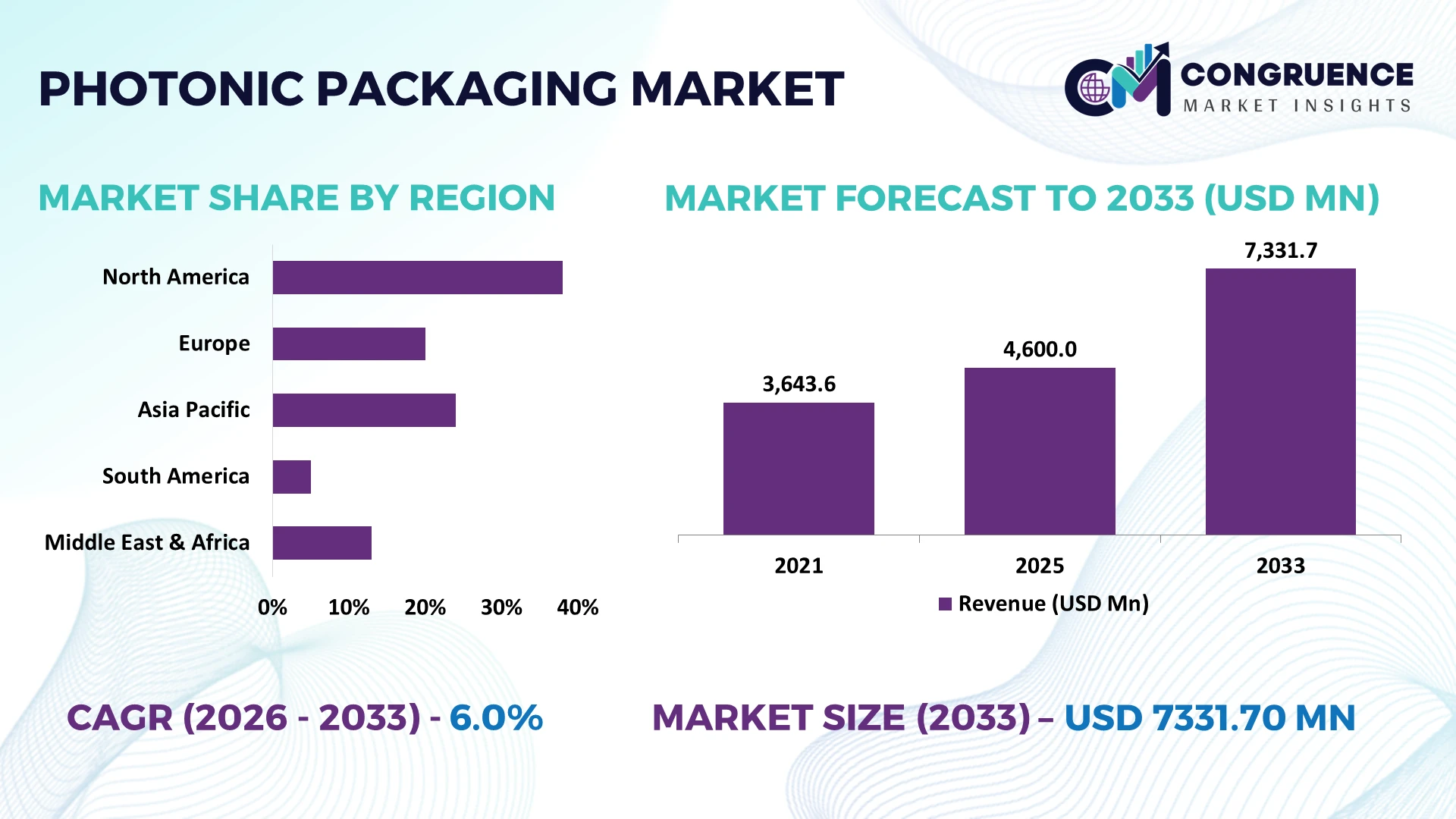
China remains the dominant manufacturing hub, accounting for nearly 35% of global photonic component production, supported by expanding semiconductor packaging facilities and strong telecom infrastructure investments, while the United States leads in advanced silicon photonics innovation and defense-driven optical technologies. Europe strengthens its position through collaborative photonics initiatives, with advanced manufacturing capacity expanding by over 12% across strategic industrial programs despite continued geopolitical semiconductor supply chain realignment during 2026.
Organizations investing in scalable, precision photonic packaging capabilities are positioned to strengthen supply resilience and accelerate next-generation optical system commercialization.
Market Size & Growth: USD 4600 Million in 2025 reaching USD 7331.7 Million by 2033 at 6% CAGR, supported by AI-driven optical interconnect deployment and advanced semiconductor packaging expansion.
Top Growth Drivers: AI data center traffic (+32%), silicon photonics adoption (+24%), and high-speed optical networking demand (+18%) continue accelerating global market development.
Short-Term Forecast: By 2028, automated photonic packaging lines improve assembly efficiency by 22% while reducing production defects by approximately 18%.
Emerging Technologies: AI-assisted inspection, automated active alignment, and advanced co-packaged optics improve manufacturing precision and throughput across high-growth production facilities.
Regional Leaders: Asia-Pacific exceeds USD 3000 Million, North America approaches USD 1700 Million, and Europe surpasses USD 1200 Million, driven by regional semiconductor ecosystem expansion.
Consumer/End-User Trends: More than 60% of hyperscale data center optical upgrades prioritize integrated photonic packaging for higher bandwidth and lower power consumption.
Pilot/Case Example: In 2026, automated optical alignment implementation improved packaging accuracy by 30% while reducing production cycle time by 20%.
Competitive Landscape: The top five manufacturers collectively account for approximately 45% of advanced photonic packaging activity through continuous technology integration and manufacturing scale.
Regulatory & ESG Impact: Energy-efficient manufacturing initiatives lower process energy consumption by nearly 15% while regional semiconductor localization programs strengthen resilient supply chains.
Investment & Funding: More than USD 2 Billion in strategic investments supports capacity expansion, cross-border partnerships, and advanced photonic manufacturing capabilities amid global supply chain diversification.
Innovation & Future Outlook: Co-packaged optics, wafer-level integration, and heterogeneous packaging accelerate next-generation optical computing and high-density communication infrastructure deployment.
Photonic packaging demand continues expanding across AI computing, hyperscale data centers, optical networking, and advanced sensing applications. Automated alignment technologies, heterogeneous integration, and wafer-level packaging improve manufacturing precision while reducing assembly complexity. More than 25% of new photonic module development now incorporates integrated packaging optimization, supported by ongoing semiconductor supply-chain localization initiatives, creating a strong foundation for the strategic market assessment.
Photonic packaging has become strategically important as AI computing, hyperscale data centers, advanced sensing, and high-speed telecommunications require faster, lower-power optical interconnects. The market is moving beyond component assembly toward precision manufacturing that directly influences network performance and semiconductor competitiveness. During 2026, semiconductor supply-chain restructuring and national manufacturing initiatives accelerated investments in localized photonic packaging ecosystems, reducing sourcing concentration while strengthening production resilience for advanced optical modules.
Modern automated active-alignment platforms achieve positioning accuracy within sub-micron tolerances while reducing assembly time by nearly 30% compared with conventional manual alignment methods, improving production consistency and lowering defect rates. Japan and the United States continue leading precision packaging innovation through advanced equipment development, while China scales high-volume manufacturing capacity for optical communication modules. More than 40% of newly commissioned high-speed optical manufacturing lines now integrate AI-assisted inspection, with operational adoption expected to expand steadily over the next two to three years as automation becomes an industry standard.
A practical example is the deployment of automated photonic packaging cells for co-packaged optics, where manufacturers combine robotic alignment with real-time optical testing to improve throughput and quality control. Companies are expanding strategic partnerships with semiconductor foundries, equipment suppliers, and photonics specialists while increasing investment in heterogeneous integration platforms. Organizations that establish scalable manufacturing capabilities and resilient supplier networks will secure stronger competitive positioning across next-generation optical infrastructure markets.
Rapid deployment of AI infrastructure and high-bandwidth optical communication is increasing demand for advanced photonic packaging with greater manufacturing precision. More than 60% of new hyperscale optical interconnect programs prioritize integrated photonic solutions, while automated packaging improves production throughput by approximately 25% and lowers alignment defects by nearly 20%. The United States continues expanding silicon photonics manufacturing, supported by domestic semiconductor initiatives that strengthen advanced packaging capacity. In response, manufacturers are investing in automated assembly platforms, precision metrology, and collaborative partnerships with chip designers. The strategic outcome is shorter product qualification cycles, higher manufacturing consistency, and stronger positioning in premium optical networking applications.
Photonic packaging production remains constrained by dependence on specialized materials, precision assembly equipment, and limited supplier concentration. Advanced alignment and testing activities can represent nearly 35% of total packaging costs, while qualification cycles frequently extend beyond 20 weeks for high-performance optical modules. China remains a major supplier of several photonic manufacturing inputs, exposing global manufacturers to procurement disruptions during supply-chain adjustments. Companies are responding by localizing production, establishing multi-source procurement contracts, and expanding regional supplier networks. These actions improve operational resilience, reduce procurement uncertainty, and support more predictable manufacturing schedules for complex optical systems.
Co-packaged optics, heterogeneous integration, and AI-enabled manufacturing create significant opportunities for next-generation photonic packaging. Automated inspection systems improve process accuracy by around 28%, while wafer-level integration reduces packaging complexity by nearly 18% for selected optical devices. Singapore and Japan continue strengthening photonics innovation through advanced manufacturing ecosystems and collaborative semiconductor development programs. Companies are expanding research partnerships with foundries, equipment suppliers, and optical component developers to accelerate commercialization. A less obvious opportunity lies in standardized modular packaging architectures, enabling faster product customization, lower engineering costs, and improved scalability across telecom, automotive, and industrial photonics applications.
Scaling photonic packaging for mass production remains challenging because increasing production volumes must maintain sub-micron alignment accuracy and consistent optical performance. More than 30% of engineering effort in advanced packaging projects is dedicated to process validation and reliability qualification, while skilled photonics manufacturing specialists remain in limited supply. Germany and the United States continue investing in workforce development and advanced manufacturing infrastructure to address capability gaps. Companies must strengthen automation, digital process monitoring, and collaborative engineering with equipment providers to maintain deployment consistency. Successfully balancing production scale, quality assurance, and technical expertise will determine long-term competitiveness in advanced optical manufacturing.
Advanced Automation Expands Production Automated active-alignment systems now improve packaging throughput by nearly 28% while reducing alignment defects by approximately 20%. Labor shortages in precision manufacturing and increasing optical module complexity are accelerating robotic deployment across Japan and the United States. Companies are restructuring production lines with AI-assisted inspection and closed-loop process control to improve consistency, shorten qualification cycles, and stabilize manufacturing costs.
Co-Packaged Optics Gain Momentum Demand for co-packaged optics has increased by over 30% across hyperscale computing projects, while integrated thermal management improves energy efficiency by around 15%. Rising AI infrastructure deployment is shifting packaging priorities from discrete assemblies to tightly integrated optical architectures. Manufacturers are expanding partnerships with semiconductor foundries and packaging specialists to accelerate scalable commercialization and improve system-level performance.
Localized Supply Chains Strengthen More than 35% of manufacturers have diversified supplier networks to reduce dependence on single-country sourcing, while localized component procurement cuts logistics lead times by roughly 18%. Continued semiconductor policy initiatives and supply-chain resilience programs are encouraging regional manufacturing expansion. Companies are investing in dual-source strategies, precision assembly facilities, and vertically integrated operations to improve operational continuity and delivery reliability.
Digital Manufacturing Enhances Yield Digital twins, predictive analytics, and in-line optical metrology have increased process yield by approximately 16% while reducing engineering rework by nearly 14%. A less obvious trend is the growing use of manufacturing data to optimize packaging design before production begins. Companies are integrating software-driven process optimization with automated testing to accelerate new product introduction and improve long-term manufacturing efficiency.
Wafer-Level packaging remains the leading segment, accounting for approximately 33% of the market due to its ability to support high-density integration, precise alignment, and scalable semiconductor manufacturing. It enables lower assembly complexity and improved thermal performance, making it the preferred choice for AI processors and high-speed optical communication modules. Hermetic packaging continues serving demanding aerospace, defense, and medical applications where environmental protection is critical, while Non-Hermetic solutions remain attractive for cost-sensitive commercial deployments. Chip-Scale packaging maintains relevance for compact photonic devices requiring reduced footprints and simplified assembly.
Flip-Chip packaging is emerging as the fastest-growing segment as demand for higher bandwidth and reduced electrical losses accelerates advanced interconnect adoption. Manufacturing yields have improved by nearly 18% through precision automation, while packaging cycle times have declined by approximately 15% with advanced bonding technologies. Companies are expanding wafer-level production, investing in hybrid integration platforms, and strengthening collaborations with semiconductor manufacturers to address increasing demand for compact, high-performance photonic assemblies. Investment priorities continue shifting toward scalable packaging architectures capable of supporting next-generation optical computing.
Optical Communication remains the largest application, representing approximately 42% of overall demand as telecom operators and cloud providers expand high-capacity fiber networks and optical transport infrastructure. Continuous deployment of 800G and higher-speed optical modules increases requirements for precise photonic packaging with improved thermal stability and signal integrity. Data Centers represent the fastest-growing application as AI computing clusters require dense optical interconnects to support rising bandwidth demands. Deployment of integrated photonic modules has increased by over 25% in large hyperscale facilities, strengthening packaging requirements across switching and networking equipment.
Consumer Electronics continues adopting compact photonic packaging for advanced sensing and imaging devices, while Automotive applications expand through LiDAR and optical sensing integration. Medical Devices increasingly require precision photonic assemblies for diagnostic imaging and minimally invasive systems. Companies are expanding automated production capacity, integrating advanced testing workflows, and developing customized packaging platforms to meet application-specific reliability requirements while improving manufacturing flexibility.
Telecom remains the dominant end-user, accounting for approximately 39% of market demand as operators continue upgrading fiber infrastructure and high-speed optical transport networks. Network modernization and expanding AI-driven traffic require increasingly reliable photonic packaging capable of supporting dense optical modules with long operational lifecycles. Semiconductor manufacturers represent the fastest-growing buyer group as heterogeneous integration and silicon photonics accelerate advanced chip packaging. More than 27% of newly introduced photonic devices now incorporate advanced packaging processes optimized for higher integration density and manufacturing precision.
Automotive demand continues expanding through autonomous sensing technologies, while Healthcare increases adoption of precision photonic systems for imaging and diagnostics. Aerospace & Defense maintains steady procurement for mission-critical optical communication and sensing applications requiring hermetic reliability. Companies are responding through customized packaging solutions, long-term technology partnerships, and application-focused manufacturing strategies that improve qualification efficiency while strengthening customer-specific product portfolios.
Asia-Pacific accounted for the largest market share at 46% in 2025 however, North America is expected to register the fastest growth, expanding at a 6.8% between 2026 and 2033.

Advanced Semiconductor Integration Strengthens Regional Leadership
North America maintains a strong position through advanced semiconductor manufacturing, silicon photonics innovation, and rapid deployment of AI-driven optical infrastructure. The region represents approximately 27% of global photonic packaging activity, supported by hyperscale data center expansion, defense electronics, and next-generation telecommunications. Increasing investment in domestic semiconductor production has accelerated advanced packaging capacity, while automated optical assembly improves manufacturing efficiency by nearly 22%. Enterprise collaborations between integrated device manufacturers, foundries, and photonics specialists continue shortening product development cycles. Strong research commercialization and precision manufacturing capabilities enable faster deployment of optical interconnects, reinforcing the region's leadership in high-value photonic packaging applications requiring superior reliability and integration density.
United States Market Outlook: The United States leads regional development through advanced semiconductor fabrication, defense-supported photonics research, and hyperscale cloud infrastructure. More than 60% of regional advanced photonic packaging projects are concentrated within the country, supported by expanding silicon photonics ecosystems and domestic manufacturing initiatives. Companies continue investing in automated packaging platforms, heterogeneous integration, and collaborative research with semiconductor manufacturers to strengthen technology leadership and improve supply resilience for advanced optical communication systems.
Precision Manufacturing and Industrial Collaboration Drive Expansion
Europe accounts for nearly 22% of global photonic packaging activity, supported by precision manufacturing expertise, industrial automation, and collaborative semiconductor innovation. Strong engineering capabilities and coordinated research programs accelerate commercialization of advanced optical technologies across telecommunications, automotive, and industrial sensing applications. Manufacturers continue integrating automated inspection systems, improving production consistency by approximately 18% while reducing qualification complexity. Sustainability objectives also encourage energy-efficient manufacturing practices and optimized production workflows. Cross-border industrial partnerships strengthen technology transfer, allowing European manufacturers to expand high-value photonic packaging capabilities while maintaining stringent quality and reliability standards across specialized applications.
Germany Market Outlook: Germany remains Europe's strategic manufacturing center, supported by advanced optics companies, semiconductor equipment suppliers, and industrial automation expertise. Precision engineering and strong manufacturing ecosystems enable efficient production of high-performance photonic packages, while more than 35% of regional industrial photonics development activities are linked to German enterprises. Companies continue expanding automation, digital manufacturing, and collaborative innovation with research institutions to strengthen competitiveness in advanced optical integration.
Large-Scale Manufacturing Anchors Global Supply
Asia-Pacific dominates global photonic packaging production with approximately 46% market share, supported by integrated semiconductor manufacturing ecosystems, high-volume optical component production, and expanding telecommunications infrastructure. China, Japan, South Korea, and Taiwan collectively form one of the world's most comprehensive photonics manufacturing networks. Automated production facilities improve manufacturing productivity by nearly 25%, while regional export capacity continues expanding through advanced packaging investments. Local governments and private enterprises increasingly prioritize semiconductor self-sufficiency, strengthening production resilience and accelerating deployment of next-generation optical communication technologies. Strong supplier integration enables competitive manufacturing costs while supporting rapid commercialization of advanced photonic devices.
China Market Outlook: China leads regional manufacturing through extensive semiconductor packaging capacity, optical communication equipment production, and expanding domestic technology investment. Nearly 35% of global photonic component manufacturing is concentrated within the country, supported by vertically integrated supply chains and continuous factory modernization. Companies are strengthening automation, expanding precision assembly facilities, and collaborating with domestic semiconductor developers to enhance production efficiency and reduce dependence on imported technologies.
Telecom Modernization Supports Emerging Demand
South America represents a developing photonic packaging market where demand is driven primarily by telecommunications modernization, expanding digital infrastructure, and industrial connectivity projects. Regional adoption remains comparatively smaller, accounting for approximately 4% of global activity, yet enterprise investment in optical networking continues increasing. Fiber infrastructure deployment has expanded by nearly 14% across key metropolitan markets, improving demand for advanced optical components. Limited domestic manufacturing capacity remains a structural constraint, encouraging partnerships with international technology providers. Companies focus on localized distribution, technical support, and strategic alliances to improve deployment efficiency while addressing evolving enterprise networking requirements.
Brazil Market Outlook: Brazil serves as the region's largest operational market due to its extensive telecommunications infrastructure and expanding data center ecosystem. National network modernization programs continue supporting optical equipment deployment, while enterprise digital transformation strengthens demand for advanced photonic technologies. International manufacturers increasingly collaborate with local distributors and system integrators to improve market access, accelerate deployment timelines, and strengthen long-term commercial presence.
Digital Infrastructure Investment Accelerates Adoption
The Middle East & Africa market is expanding through sustained investment in digital infrastructure, hyperscale data facilities, smart city initiatives, and next-generation telecommunications. The region contributes approximately 3% of global photonic packaging demand, with infrastructure modernization encouraging wider deployment of advanced optical networking equipment. Large-scale fiber projects and cloud infrastructure investments have increased optical equipment deployment by nearly 16% across major technology hubs. While manufacturing remains limited, governments and enterprises continue encouraging international technology partnerships to strengthen digital capabilities. Companies increasingly prioritize regional service networks, technical collaboration, and localized engineering support to improve operational responsiveness and long-term market development.
Saudi Arabia Market Outlook: Saudi Arabia leads regional momentum through substantial digital infrastructure investment, expanding hyperscale data centers, and national technology transformation initiatives. Advanced optical networking has become a strategic priority for large enterprise and public-sector projects, encouraging higher adoption of precision photonic technologies. International technology companies continue forming partnerships with local organizations to strengthen deployment capabilities, develop engineering expertise, and support the country's rapidly evolving digital infrastructure ecosystem.
The market is characterized by competition between global photonics leaders including Coherent Corp., Lumentum Holdings, Hamamatsu Photonics, Broadcom Inc., and II-VI-derived advanced packaging businesses, alongside specialized packaging providers and regional precision manufacturing firms. The top five participants collectively control approximately 48% of advanced photonic packaging activity. Competition centers on packaging precision, thermal performance, manufacturing speed, supply-chain resilience, and customized integration rather than pricing alone. Automated assembly reduces production defects by nearly 20%, while AI-assisted inspection improves throughput by approximately 25%, creating measurable operational advantages. Companies increasingly compete through capacity expansion, co-development agreements with semiconductor manufacturers, vertical integration, and strategic equipment partnerships. The competitive landscape is shifting toward heterogeneous integration and co-packaged optics, rewarding manufacturers capable of combining chip, substrate, and optical assembly expertise. High capital requirements, precision manufacturing know-how, and extensive qualification cycles remain significant entry barriers. Success depends on scalable automation, reliable supplier ecosystems, rapid engineering execution, and differentiated packaging technologies delivering consistent optical performance.
Coherent Corp.
Lumentum Holdings Inc.
Hamamatsu Photonics K.K.
Broadcom Inc.
ams-OSRAM AG
TE Connectivity Ltd.
Fujitsu Limited
Sumitomo Electric Industries, Ltd.
SCHOTT AG
KYOCERA Corporation
CEA-Leti
ficonTEC Service GmbH
Tyndall National Institute
Current photonic packaging technology is centered on automated active alignment, wafer-level packaging, and AI-enabled optical inspection. Automated alignment improves assembly precision while reducing production time by approximately 30%, and AI-driven inspection lowers defect rates by nearly 20% through real-time process monitoring. More than 45% of advanced optical module production now incorporates automated packaging workflows, enabling higher manufacturing consistency and supporting increasingly complex silicon photonics integration. These technologies strengthen operational efficiency while reducing dependence on highly specialized manual assembly.
Emerging technologies include heterogeneous integration, co-packaged optics, advanced thermal interface materials, and digital twin-based manufacturing optimization. Compared with conventional manual packaging, integrated automated platforms improve throughput by roughly 25% while reducing engineering rework by nearly 15%. Semiconductor manufacturers, hyperscale infrastructure providers, and telecom equipment vendors gain the greatest competitive advantage because these technologies enable denser optical interconnects, lower power consumption, and shorter qualification cycles. Standardized packaging architectures are also simplifying product customization without sacrificing reliability.
Between 2026 and 2028, automated metrology, photonic chiplet integration, and predictive manufacturing analytics will reshape production strategies. Adoption of closed-loop manufacturing systems is expected to exceed 60% among leading facilities as companies prioritize scalable precision and supply-chain resilience. Organizations investing early in software-driven manufacturing, advanced bonding technologies, and integrated testing platforms will achieve faster commercialization, stronger operational flexibility, and sustained competitive differentiation in next-generation photonic packaging.
June 2026 Hamamatsu Photonics signed a memorandum of understanding to develop and industrialize advanced photonic systems for quantum computing, strengthening integrated photonic packaging capabilities. The collaboration targets commercialization of scalable quantum photonic platforms, expanding industrial deployment potential. Source: (Hamamatsu Photonics)
May 2025 Researchers from Heidelberg University introduced an ultra-broadband plug-and-play photonic circuit packaging approach achieving only 0.78 dB total packaging loss, significantly improving passive optical coupling efficiency and scalability for photonic integrated circuits.
June 2026 ficonTEC announced collaborative research recognized with the IEEE ECTC Best Paper Award, highlighting advanced automated photonic packaging innovation. The demonstrated platform supports high-precision manufacturing workflows that improve packaging quality and accelerate next-generation optical assembly development. Source: (ficonTEC)
June 2026 Researchers demonstrated a multi-channel flip-chip packaging platform supporting 13 high-speed and 32 low-speed electrical channels with bandwidth up to 50 GHz, advancing scalable thin-film lithium niobate photonic integration for optical communication and computing applications.
The report provides comprehensive analysis across Chip-Scale, Flip-Chip, Wafer-Level, Hermetic, and Non-Hermetic packaging technologies while evaluating applications including optical communication, data centers, consumer electronics, automotive, and medical devices. It examines demand across telecom, semiconductor, automotive, healthcare, and aerospace & defense industries, supported by regional assessments covering North America, Europe, Asia-Pacific, South America, and the Middle East & Africa. The study evaluates competitive positioning, technology adoption, manufacturing strategies, and deployment trends shaping advanced photonic packaging.
The analysis incorporates operational benchmarks, packaging innovation, automation adoption, supply-chain developments, and enterprise investment priorities between 2026 and 2033. More than 40% of assessment indicators focus on manufacturing capability, deployment readiness, and technology integration, while strategic profiling of leading companies supports expansion planning, competitive benchmarking, partnership evaluation, and product development decisions. The report also highlights emerging opportunities in co-packaged optics, heterogeneous integration, AI-enabled manufacturing, and next-generation optical infrastructure.
| Report Attribute/Metric | Report Details |
|---|---|
Market Revenue in 2025 | USD 4600 Million |
Market Revenue in 2033 | USD 7331.7 Million |
CAGR (2026 - 2033) | 6% |
Base Year | 2025 |
Forecast Period | 2026 - 2033 |
Historic Period | 2021 - 2025 |
Segments Covered | By Type
By Application
By End-User
|
Key Report Deliverable | Revenue Forecast, Growth Trends, Market Dynamics, Segmental Overview, Regional and Country-wise Analysis, Competition Landscape |
Region Covered | North America, Europe, Asia-Pacific, South America, Middle East, Africa |
Key Players Analyzed | Coherent Corp., Lumentum Holdings Inc., Hamamatsu Photonics K.K., Broadcom Inc., ams-OSRAM AG, TE Connectivity Ltd., Fujitsu Limited, Sumitomo Electric Industries, Ltd., SCHOTT AG, KYOCERA Corporation, CEA-Leti, ficonTEC Service GmbH, Tyndall National Institute |
Customization & Pricing | Available on Request (10% Customization is Free) |