
Reports
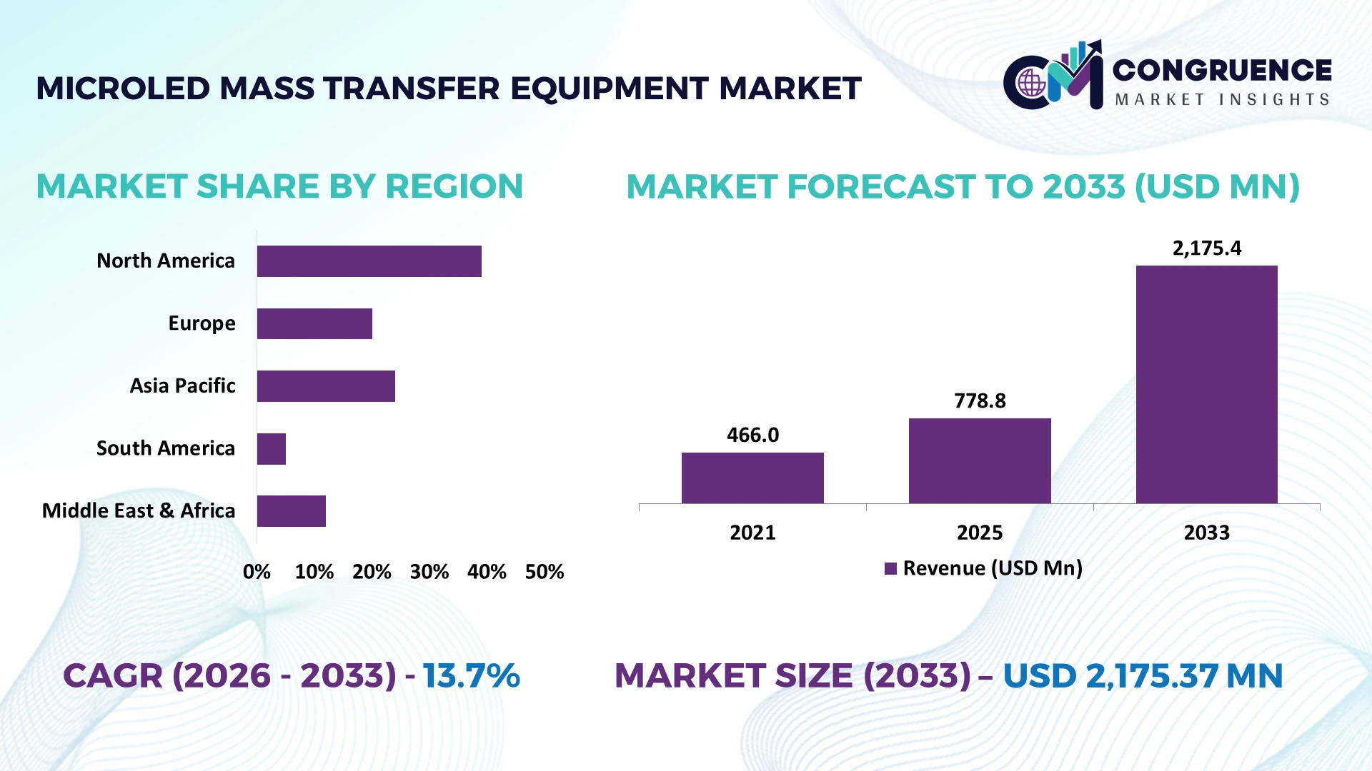
The Global MicroLED Mass Transfer Equipment Market was valued at USD 778.84 Million in 2025 and is anticipated to reach a value of USD 2175.37 Million by 2033 expanding at a CAGR of 13.7% between 2026 and 2033. Growth is driven by laser-assisted transfer exceeding 50,000 dies per second, automated defect inspection, wafer-to-panel architectures, and the requirement to transfer millions of sub-50-micrometer LEDs at production-grade yields.
South Korea represents a strategically important MicroLED transfer technology hub, accounting for approximately 42% of 4,813 major global transfer-technology patent filings, compared with China at about 23%. Korean companies LG Electronics and Samsung Electronics recorded 648 and 503 filings, respectively, while the government committed KRW 484 billion toward next-generation inorganic LED technologies through 2032. Premium televisions, automotive displays, AR/VR systems, and wearable devices remain priority applications. U.S.–China technology localization pressures are simultaneously encouraging Asian manufacturers to strengthen domestic equipment, materials, and process-control capabilities.
For equipment suppliers and display manufacturers, early qualification of high-throughput laser transfer, automated inspection, and repair platforms is critical to securing production programs before MicroLED manufacturing shifts from pilot lines toward larger commercial volumes.
Market Size & Growth: USD 778.84 million in 2025 is projected to reach USD 2,175.37 million by 2033 at 13.7% CAGR, supported by high-throughput laser transfer and increasingly automated MicroLED assembly.
Top Growth Drivers: Laser-assisted transfer represents nearly 32% of equipment activity, wafer-to-panel platforms account for approximately 46.37%, and consumer-electronics applications contribute about 54.21% of equipment demand.
Short-Term Forecast: By 2028, advanced production lines will increasingly target transfer speeds above 50,000 dies per second while automated optical inspection pushes defect detection toward sub-0.5% levels, reducing rework intensity.
Emerging Technologies: Laser-induced forward transfer, AI-enabled machine vision, hybrid electrostatic transfer, and automated repair systems are replacing slower mechanical approaches; advanced laser platforms already deliver roughly 10× higher transfer speeds than conventional stamp-based processes.
Regional Leaders: Asia-Pacific held approximately 62.83% of 2025 equipment activity, while North America accelerates advanced-packaging and MicroLED pilot infrastructure and Europe maintains roughly 8% participation concentrated around automotive, aerospace, and R&D applications.
Consumer/End-User Trends: Consumer electronics accounted for approximately 54.21% of equipment demand in 2025, while AR/VR manufacturing is increasingly shifting toward sub-10-micrometer emitters requiring substantially tighter placement accuracy and defect control.
Pilot/Case Example: In 2025–2026, laser-transfer equipment demonstrated throughput above 50,000 dies per second with approximately 99.7% placement performance within 0.6-micrometer alignment tolerances, strengthening commercial-scale manufacturing economics.
Competitive Landscape: Elastomer-stamp equipment retained approximately 41.68% share by transfer technology in 2025, while ASMPT, Coherent, Toray Engineering, Kulicke & Soffa, and PlayNitride compete through throughput, precision, inspection integration, and repair capability.
Regulatory & ESG Impact: South Korea's KRW 484 billion inorganic-LED development program extends through 2032, strengthening domestic MicroLED chips, materials, transfer processes, and manufacturing infrastructure while reducing dependence on imported critical display technologies.
Investment & Funding: Chinese display manufacturers Tianma, BOE, and Visionox collectively committed more than USD 1.5 billion to pilot and Gen 4.5 infrastructure during 2024–2025, reinforcing Asia's equipment qualification ecosystem and localized supply chain.
Innovation & Future Outlook: MicroLED applications are expected to expand from approximately 30,000 units in 2024 toward 440,000 units by 2030, intensifying requirements for scalable transfer, inspection, repair, and yield-management systems across global display manufacturing.
MicroLED mass transfer equipment is becoming a manufacturing control point for premium televisions, automotive cockpits, augmented-reality displays, smart wearables, and high-brightness commercial panels. Laser-assisted transfer exceeding 50,000 dies per second is reshaping production economics, while wafer-to-panel architectures already represent about 46% of equipment deployment. AI-driven inspection, selective laser repair, and hybrid transfer heads are reducing defect-related rework and enabling smaller emitters. Against continued semiconductor and display supply-chain localization, equipment vendors with integrated transfer, metrology, and repair capability are positioned for the next strategic phase of MicroLED commercialization.
MicroLED mass transfer equipment is becoming strategically important because transfer yield, placement accuracy, and repair throughput increasingly determine whether display makers can move from demonstration panels to repeatable volume manufacturing. A single 4K RGB display requires transferring roughly 25 million individual emitters, making equipment productivity a direct competitive variable. Supply-chain localization in South Korea, Taiwan, and China is consequently shifting investment toward integrated transfer, inspection, bonding, and repair lines rather than isolated process tools.
Laser-assisted transfer systems can process above 50,000 dies per second, delivering approximately 10× the throughput of conventional stamp-based approaches while maintaining micron-scale placement control. South Korea leads in transfer-related intellectual property and premium display integration, while China is emphasizing production capacity and localized equipment ecosystems. Taiwan remains important in semiconductor-display integration, particularly for microdisplays and advanced packaging.
A practical production line combines laser transfer with automated optical inspection to identify misplaced or defective emitters and selectively repair them without reprocessing complete panels. Through 2028, commercial platforms will increasingly target >99.99% effective post-repair yield and tighter sub-micron alignment. Equipment companies are therefore prioritizing laser technology, machine vision, process integration, and display-maker partnerships. Competitive advantage will belong to suppliers that convert transfer speed into stable yield and lower repair intensity.
Mass-transfer productivity is the primary structural driver because MicroLED commercialization requires millions of microscopic emitters to be positioned with near-zero defect tolerance. Advanced laser platforms exceed 50,000 dies per second, while production processes increasingly target transfer yields above 99.9% and placement accuracy approaching ±1 micrometer. Compared with sequential pick-and-place architectures, parallel and laser-assisted methods can improve throughput by more than 80%, materially reducing takt time. South Korea's next-generation display strategy and China's localized display-equipment expansion are accelerating qualification of domestic transfer platforms. Equipment manufacturers are responding by integrating laser transfer, automated optical inspection, alignment correction, and selective repair into unified cells. The strategic shift is clear: display producers increasingly evaluate equipment on usable yield per hour, not headline transfer speed alone.
Production economics remain constrained by the extreme defect sensitivity created when millions of MicroLED chips are transferred onto one backplane. Even a 99.99% initial transfer yield produces roughly 2,500 defective placements across a 25-million-emitter RGB 4K configuration, making inspection and repair unavoidable. Transfer equipment can represent approximately 20–30% of specialized MicroLED assembly-line capital requirements, while sub-micron alignment and environmental controls increase facility complexity. Dependence on precision lasers, optical components, motion stages, and semiconductor-grade metrology also exposes manufacturers to concentrated Japanese, German, and U.S. component supply chains. Producers are mitigating these constraints through modular equipment architectures, multisourcing, localized component qualification, and contractual supplier relationships. Operationally, reducing defect-generation frequency delivers greater economic value than simply increasing nominal transfer throughput.
The strongest opportunity lies in equipment architectures combining transfer, metrology, AI inspection, defect mapping, and selective repair within a closed-loop production workflow. Machine-vision systems can inspect millions of emitters rapidly, while laser-based selective processing can eliminate more than 90% of unnecessary manual intervention in highly automated configurations. Wafer-to-panel architectures already represent roughly 46% of equipment deployment, creating opportunities for larger transfer fields and fewer handling stages. Taiwan's semiconductor packaging ecosystem provides a particularly attractive pathway for integrating MicroLED assembly with wafer-level processing, silicon backplanes, and AR microdisplay manufacturing. Equipment developers are increasing R&D around adaptive laser control, digital process recipes, and automated repair. A non-obvious opportunity is software monetization: yield analytics and recipe optimization can create recurring value beyond one-time equipment sales.
Long-term competitiveness depends on maintaining transfer accuracy, thermal stability, inspection reliability, and repair performance as emitter dimensions move below 10 micrometers. At these dimensions, a displacement of only 1 micrometer can represent more than 10% of die width, increasing sensitivity to vibration, substrate distortion, laser-energy variation, and backplane registration errors. Production systems simultaneously need effective post-repair yields approaching 99.99% while processing tens of thousands of dies each second. Scaling laboratory performance across multi-shift factories therefore creates a process-control challenge distinct from equipment cost. Japan, South Korea, and Taiwan also face shortages of engineers spanning photonics, precision motion, semiconductor packaging, and display integration. Suppliers must invest in predictive calibration, closed-loop metrology, digital twins, workforce development, and joint qualification laboratories to deliver consistent performance across customer sites.
Laser Transfer Moves Into Production: Laser-assisted systems are moving from qualification toward production, with advanced platforms exceeding 50,000 dies per second and approaching sub-micron placement tolerances. Manufacturers are combining laser release with inline alignment and defect mapping, shortening transfer cycles by over 60%. Taiwanese and South Korean suppliers are expanding joint process-development programs to accelerate customer qualification.
Closed-Loop Yield Control Expands: Transfer cells increasingly integrate automated optical inspection, machine vision, and selective repair instead of treating inspection as a downstream operation. AI-supervised systems can identify defect levels below 0.5%, while automated repair workflows reduce repeated panel handling by roughly 30–40%. Equipment companies are integrating metrology software directly into transfer platforms to improve usable output per production hour.
Application-Specific Lines Replace Standardization: MicroLED manufacturers are shifting toward dedicated equipment configurations for televisions, automotive displays, wearables, and microdisplays because emitter dimensions now range from below 5 µm to above 50 µm. In China, automotive panel shipments expanded nearly 10% in 2024, encouraging equipment suppliers to offer modular optics, configurable transfer heads, and application-specific bonding recipes.
Pilot Lines Transition Toward Commercialization: Production strategies are changing from laboratory demonstrations to low-volume commercial lines. AUO's G4.5 infrastructure supports MicroLED smartwatch and automotive programs, while AR products represented 58% of MicroLED display activity measured by Counterpoint Research in 2025. Companies are prioritizing scalable pilot capacity, customer co-development, and flexible tooling before committing to larger manufacturing footprints.
Stamp Transfer Systems remain the leading type, accounting for approximately 41.7% of 2025 equipment activity. Their dominance reflects mature elastomeric handling, relatively low consumable costs, compatibility with 10–20 µm dies, and transfer rates around 10,000–20,000 dies per second. Pick-and-Place Systems retain strategic relevance for prototype development, repair, and low-volume heterogeneous integration where individual die control outweighs throughput requirements. Roll-to-Roll Systems remain specialized, primarily supporting flexible-substrate development rather than mainstream rigid-panel manufacturing.
Laser Transfer Systems represent the fastest adoption shift among the listed technologies, capturing nearly one-third of equipment activity as manufacturers pursue non-contact processing, >50,000-die-per-second throughput, and tighter sub-micron alignment. Electrostatic Transfer Systems remain smaller but increasingly complement laser or mechanical architectures where controlled landing forces are required. Equipment suppliers are consequently redirecting engineering investment toward laser optics, configurable transfer heads, automated calibration, and hybridized process modules. The business implication is a gradual migration from mechanically optimized platforms toward software-controlled, non-contact architectures capable of handling smaller emitters without sacrificing production speed.
Television Displays remain the largest equipment-intensive application, representing an estimated 32–35% of deployment because large-format panels require millions of RGB emitters, extensive transfer fields, and repeated inspection-repair cycles. Display Assembly remains strategically important across multiple product categories, particularly where transfer, bonding, testing, and repair are integrated into one production architecture. MicroLED Displays used in signage and premium commercial installations continue supporting mature equipment utilization because large pixel pitches reduce transfer complexity relative to near-eye devices.
Wearable Displays represent the fastest-growing application shift as commercial smartwatch launches validate smaller, high-brightness MicroLED panels. Wearables increasingly require emitters below 20 µm, pushing suppliers toward high-precision laser transfer and denser inspection workflows. Automotive Displays are simultaneously strengthening through transparent displays, cockpit modules, and exterior communication surfaces, while television manufacturers focus on reducing panel cost and repair intensity. Companies are therefore separating equipment configurations by die size and substrate format rather than relying on universal transfer platforms. This application fragmentation increases demand for modular tooling and recipe-based automation.
Display Manufacturers constitute the dominant end-user group, representing approximately 45–50% of equipment procurement because they operate the transfer, bonding, inspection, repair, and backplane integration infrastructure required for commercial MicroLED production. Consumer Electronics Companies typically participate through specification development, co-investment, and supply agreements rather than owning every process stage. Semiconductor Manufacturers are gaining importance as MicroLED production adopts wafer-level processing, CMOS integration, and semiconductor-grade metrology, particularly for high-pixel-density microdisplays.
Automotive Electronics Companies are the fastest-expanding buyer group as vehicle platforms adopt larger, brighter, and more durable display architectures. Total automotive center-display area increased 19% during 2025, while 15–20-inch displays increased their share from 7% to 11%, strengthening requirements for precision assembly and reliable high-temperature operation. Research Institutes remain important for emerging transfer physics, novel materials, and sub-10 µm device development. Equipment suppliers are responding with configurable research platforms, joint development agreements, automotive-qualified process modules, and semiconductor-compatible systems, shifting competitive positioning toward ecosystem integration rather than standalone machine sales.
Asia-Pacific accounted for the largest market share at approximately 63% in 2025 however, North America is expected to register the fastest growth, expanding at a CAGR of approximately 15% between 2026 and 2033.
Advanced Microdisplay Integration Accelerates Equipment Qualification
North America accounts for approximately 18% of MicroLED mass transfer equipment activity, with deployment concentrated around semiconductor-grade microdisplays, AR systems, defense electronics, advanced packaging, and specialized display development. The region's advantage is process integration rather than high-volume television-panel manufacturing. U.S. technology programs increasingly combine MicroLED epitaxy, CMOS backplanes, wafer-level bonding, laser transfer, and automated inspection, creating demand for equipment capable of sub-10 µm emitter handling. Federal semiconductor localization initiatives are also strengthening domestic photonics and advanced-packaging infrastructure. Applied Materials' planned EPIC Center in California represents a USD 4 billion semiconductor R&D investment and is designed to support more than 2,000 engineering positions, reinforcing the process-development ecosystem available to next-generation display technologies. Equipment vendors are consequently targeting research fabs and specialty manufacturers through configurable platforms and joint process qualification.
United States Market Outlook: The United States combines semiconductor fabrication, photonics expertise, AR development, and defense-grade microelectronics demand. The CHIPS ecosystem has mobilized tens of billions of dollars for domestic semiconductor manufacturing and R&D, expanding infrastructure relevant to MicroLED process integration. Equipment demand centers on high-precision transfer, wafer bonding, metrology, and automated defect correction rather than commodity display assembly.
Semiconductor Integration Shapes Specialized Equipment Demand
Europe represents approximately 8% of MicroLED mass transfer equipment activity, with Germany, France, Belgium, and the United Kingdom emphasizing semiconductor integration, automotive displays, photonics, and microdisplay research. European deployment differs from Asian volume manufacturing because equipment specifications prioritize process flexibility, traceability, energy efficiency, and compatibility with semiconductor-grade production. The European Chips Act targets more than EUR 43 billion of policy-driven public and private investment, strengthening pilot-line and advanced-device infrastructure that can support MicroLED development. Automotive digitalization adds another equipment pathway as European OEMs evaluate high-brightness displays for cockpits, head-up systems, and exterior communication. Equipment providers are responding through collaborative R&D, modular transfer platforms, and partnerships with research institutes, enabling customers to qualify laser transfer and heterogeneous integration before committing to larger production installations.
Germany Market Outlook: Germany's strategic advantage comes from its automotive electronics, precision automation, optics, and semiconductor equipment base. The country's automotive industry produces more than 4 million passenger vehicles annually, providing a substantial qualification environment for next-generation display systems. MicroLED equipment suppliers can leverage German expertise in machine vision, motion control, industrial lasers, and automotive reliability testing to develop production-ready transfer architectures.
Display Manufacturing Scale Drives Equipment Leadership
Asia-Pacific controls approximately 63% of MicroLED mass transfer equipment activity, reflecting its concentration of display fabrication, semiconductor packaging, LED manufacturing, and production-equipment ecosystems. South Korea leads transfer-related intellectual property, China is scaling localized display infrastructure, while Taiwan combines LED manufacturing with semiconductor-grade packaging and backplane capabilities. South Korea accounts for roughly 42% of major MicroLED transfer-related patent filings, compared with approximately 23% for China, demonstrating the region's depth beyond manufacturing capacity. China simultaneously continues qualification of domestic laser, inspection, bonding, and repair equipment as technology localization reshapes procurement. Taiwan's established display and semiconductor supply chains support rapid pilot-to-production transitions. Suppliers including Toray Engineering and ASMPT are consequently emphasizing high-throughput transfer, automated inspection, and integrated repair systems designed for Asian production environments where equipment utilization and yield determine investment returns.
South Korea Market Outlook: South Korea combines Samsung and LG's display commercialization capabilities with a dense semiconductor, equipment, materials, and research ecosystem. Korean entities account for roughly 42% of major MicroLED transfer-technology patent filings, with LG Electronics and Samsung Electronics holding hundreds of filings individually. National next-generation display programs are reinforcing domestic equipment development, giving suppliers direct access to demanding television, automotive, and microdisplay qualification programs.
Premium Display Adoption Precedes Local Manufacturing
South America represents approximately 3% of global equipment activity, with demand centered on research laboratories, electronics engineering, display integration, and imported premium-display ecosystems rather than dedicated MicroLED fabrication. Brazil provides the largest industrial base through electronics manufacturing clusters in Manaus and São Paulo, while automotive production creates longer-term demand for advanced cockpit and information displays. Brazil manufactures more than 2 million vehicles annually, establishing an addressable downstream environment for high-brightness automotive display integration. However, limited compound-semiconductor fabrication and specialized transfer infrastructure restrict near-term installation of full production lines. Equipment vendors therefore prioritize university laboratories, application-development centers, and multinational electronics facilities using modular or research-scale platforms. Partnerships with international technology providers offer a more viable entry route than building standalone mass-production capacity before local MicroLED supply chains mature.
Brazil Market Outlook: Brazil offers the strongest South American pathway through its electronics assembly base, automotive industry, technical universities, and Manaus Free Trade Zone. Annual vehicle production above 2 million units supports eventual automotive-display qualification, while local electronics operations provide integration capability. Near-term equipment opportunities favor laboratory transfer systems, inspection tools, prototyping platforms, and application engineering rather than high-volume MicroLED fabs.
Digital Infrastructure Investment Creates Specialized Demand
Middle East & Africa accounts for approximately 2–3% of MicroLED mass transfer equipment activity, with adoption concentrated in research, premium digital displays, smart-city infrastructure, defense electronics, and emerging semiconductor programs. Saudi Arabia and the UAE are using economic-diversification programs to build electronics, AI, advanced-manufacturing, and semiconductor capabilities, creating an institutional base for future MicroLED development. Saudi Arabia's National Semiconductor Hub targets more than 50 semiconductor design companies by 2030, while the UAE continues expanding technology-oriented industrial infrastructure. Current equipment requirements favor laboratory-scale transfer, characterization, packaging, and prototype systems because local LED epitaxy and display-panel fabrication remain limited. International equipment companies are addressing the market through research partnerships, technical training, and configurable platforms rather than immediate high-volume installations, aligning capital deployment with developing engineering capability.
Saudi Arabia Market Outlook: Saudi Arabia offers the strongest emerging manufacturing pathway as Vision 2030 directs investment toward semiconductor design, advanced electronics, photonics, and localized technology capabilities. The National Semiconductor Hub's target of more than 50 design companies provides an ecosystem foundation for compound-semiconductor and display research. Initial MicroLED equipment demand will concentrate around universities, R&D centers, prototyping facilities, and specialized electronics programs.
ASMPT, Toray Engineering, Coherent, Kulicke & Soffa, and X Display compete through differentiated transfer architectures, while specialist equipment developers challenge established semiconductor-tool suppliers on precision and application customization. The top five players collectively control approximately 55–60% of commercial equipment activity, reflecting strong intellectual-property and qualification barriers. Stamp-based platforms retain roughly 42% technology share, but laser systems have approached one-third as customers prioritize non-contact transfer and higher throughput. Leading laser architectures deliver more than 50,000 dies per second, shifting competition from mechanical handling toward optical control, inline metrology, and software-defined process optimization. Players are securing positions through display-maker partnerships, integrated inspection-repair modules, application-specific tooling, and semiconductor-compatible automation. Supply-chain control over precision lasers, motion systems, and optical components is becoming strategically important. Customer qualification cycles and sub-micron process expertise remain formidable entry barriers. Winning requires proven yield, scalable throughput, integrated defect management, and rapid customization across television, automotive, wearable, and microdisplay production environments.
ASMPT
Toray Engineering Co., Ltd.
Coherent Corp.
Kulicke & Soffa Industries, Inc.
X Display Company
TDK Corporation
TOWA Corporation
Besi
EV Group
SÜSS MicroTec SE
SCREEN Holdings Co., Ltd.
Onto Innovation Inc.
Current MicroLED manufacturing relies on elastomer stamp transfer, precision pick-and-place, and mass bonding, but laser-induced forward transfer is changing throughput economics. ASMPT’s AD300Pro can bond more than 300,000 MicroLEDs in one pass with ±2 µm placement accuracy. Laser approaches move thousands of dies per shot, delivering above 90% throughput improvement versus sequential single-die placement. Integrated inspection and bonding increasingly determine usable yield rather than nominal transfer speed.
Emerging platforms combine excimer-laser LIFT, machine vision, adaptive binning, and closed-loop defect repair. Holst Centre demonstrated submicron transfer precision and greater than 99.9% yield across more than 10,000 MicroLEDs, signaling readiness for higher-density manufacturing. Toray Engineering integrates transfer equipment with photoluminescence inspection and laser repair, allowing defect coordinates to flow between processes. This integration reduces manual handling, improves repair efficiency by roughly 30%, and benefits suppliers offering process cells over standalone machines.
Disruptive development is shifting toward direct wafer-to-backplane laser transfer, fluidic self-assembly, and hybrid bonding for sub-10-µm emitters. By 2026–2028, production qualification will increasingly require >99.99% post-repair yield, sub-micron registration, and software-controlled process traceability. Equipment vendors investing now in laser optics, automated metrology, configurable recipes, and integrated repair gain faster customer qualification and stronger positioning across AR, automotive, wearable, and premium-display programs.
April 2024 Toray Engineering partnered with Advantest to integrate MicroLED inspection, transfer, mounting, and manufacturing-data analysis workflows. The collaboration connects multiple production stages through unified data linkage, targeting higher manufacturing efficiency and faster defect-management decisions. Source: toray-eng.com
July 2024 Coherent advanced excimer-based laser-induced forward transfer as an industrial MicroLED manufacturing route, demonstrating ±1.5 µm placement accuracy while transferring thousands of dies per laser shot. The architecture addresses the throughput limitations of conventional single-die semiconductor bonders. Source: coherent.com
September 2025 Holst Centre demonstrated laser-assisted MicroLED transfer with submicron precision and greater than 99.9% yield across more than 10,000 devices. Its adaptive-pitch release architecture supports high-density wafers, strengthening die-on-demand processing for advanced display and photonics manufacturing. Source: techblick.com
July 2026 Pixel-Flo secured £5.25 million in initial equity funding to commercialize Continuous-Flo fluidic MicroLED mass transfer. The University of Sheffield spinout uses continuous slot-die assembly for single-step RGB placement, creating an alternative pathway to conventional mechanical transfer architectures. Source: pixel-flo.com
The report evaluates MicroLED mass transfer equipment across Pick-and-Place Systems, Laser Transfer Systems, Stamp Transfer Systems, Electrostatic Transfer Systems, and Roll-to-Roll Systems. Application coverage includes Display Assembly, MicroLED Displays, Wearable Displays, Television Displays, and Automotive Displays, while end-user analysis examines Display Manufacturers, Consumer Electronics Companies, Semiconductor Manufacturers, Automotive Electronics Companies, and Research Institutes. Stamp-based platforms account for roughly 42% of current technology deployment, while laser architectures are strengthening as emitter dimensions move below 10 µm.
Geographic coverage spans North America, Europe, Asia-Pacific, South America, and Middle East & Africa, with Asia-Pacific representing approximately 63% of equipment activity. The assessment examines transfer throughput, placement precision, defect inspection, repair automation, hybrid bonding, and wafer-to-panel integration. Strategic analysis through 2033 supports equipment investment planning, geographic expansion, supplier benchmarking, technology partnerships, capacity decisions, and competitive positioning as MicroLED manufacturing transitions from specialized pilot environments toward increasingly automated commercial production.
| Report Attribute/Metric | Report Details |
|---|---|
Market Revenue in 2025 | USD 778.84 Million |
Market Revenue in 2033 | USD 2175.37 Million |
CAGR (2026 - 2033) | 13.7% |
Base Year | 2025 |
Forecast Period | 2026 - 2033 |
Historic Period | 2021 - 2025 |
Segments Covered | By Type
By Application
By End-User
|
Key Report Deliverable | Revenue Forecast, Growth Trends, Market Dynamics, Segmental Overview, Regional and Country-wise Analysis, Competition Landscape |
Region Covered | North America, Europe, Asia-Pacific, South America, Middle East, Africa |
Key Players Analyzed | ASMPT, Toray Engineering Co., Ltd., Coherent Corp., Kulicke & Soffa Industries, Inc., X Display Company, TDK Corporation, TOWA Corporation, Besi, EV Group, SÜSS MicroTec SE, SCREEN Holdings Co., Ltd., Onto Innovation Inc. |
Customization & Pricing | Available on Request (10% Customization is Free) |