
Reports
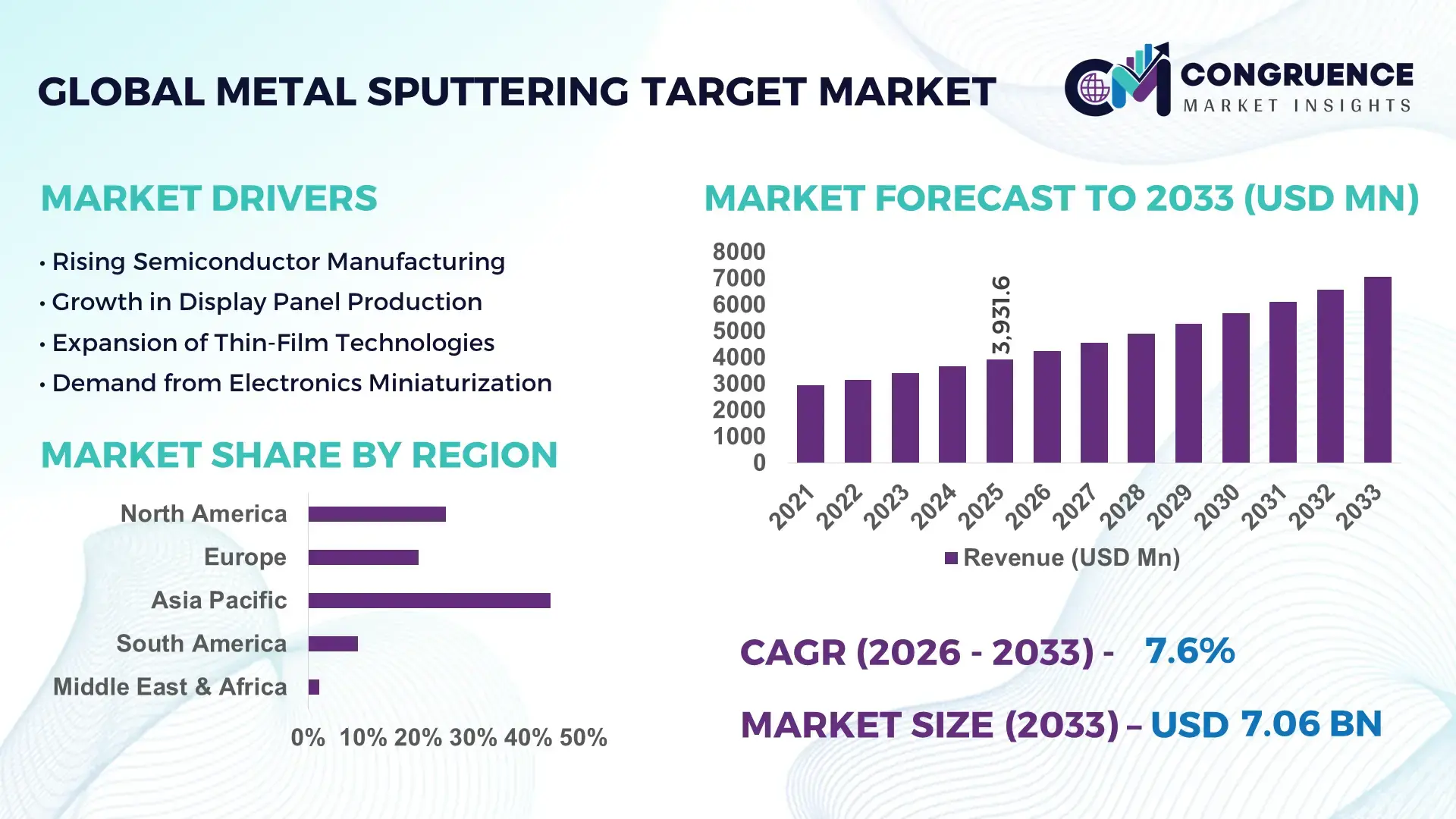
The Global Metal Sputtering Target Market was valued at USD 3931.5757408 Million in 2025 and is anticipated to reach a value of USD 7064.22978148706 Million by 2033 expanding at a CAGR of 7.6% between 2026 and 2033. This growth is driven by expanding demand for thin-film coatings in advanced electronics and optical applications.
China has established extensive capacity in metal sputtering target production, with annual output exceeding 250,000 kg of high-purity targets and capital investment in excess of USD 400 million across multiple fabrication hubs. The country’s facilities support diverse end-applications ranging from flat-panel displays and solar PV cells to semiconductor wafer processing, with technological advancements such as ultra-high-purity target engineering (>99.99 %) and real-time process quality analytics integrated into manufacturing lines. China’s R&D initiatives have produced next-generation alloys that improve deposition rates by over 18 % and reduce defect densities in coatings for consumer electronics.
Market Size & Growth: Valued at ~USD 3.93 B in 2025, projected to ~USD 7.06 B by 2033 at a 7.6 % CAGR, supported by growing electronics and energy storage sectors.
Top Growth Drivers: Expansion in display manufacturing (22 %), adoption in semiconductor fabs (18 %), efficiency improvement in coating processes (15 %).
Short-Term Forecast: By 2028, expected 12 % reduction in production costs and 14 % improvement in target utilization efficiency.
Emerging Technologies: Development of nanostructured target materials; AI-assisted sputtering process control; hybrid PVD/ALD integration.
Regional Leaders: Asia Pacific ~USD 3.1 B by 2033 with rapid consumer electronics fabrication; North America ~USD 1.4 B with advanced semiconductors; Europe ~USD 1.0 B in automotive sensors and optics coating uptake.
Consumer/End-User Trends: High adoption in flat-panel displays, advanced optics, MEMS sensors, and emerging AR/VR devices.
Pilot or Case Example: 2025 pilot in semiconductor processing yielded 17 % throughput gain and 9 % energy savings in sputtering lines.
Competitive Landscape: Market leader ~28 % share; other major competitors include global and regional specialty target manufacturers.
Regulatory & ESG Impact: Increasing environmental standards for emissions and waste handling, incentives for energy-efficient coating technologies.
Investment & Funding Patterns: Over USD 150 million in recent targeted capital expenditure for advanced fabrication and automation solutions.
Innovation & Future Outlook: Focus on additive manufacturing of targets, recyclable target materials, and integration of predictive maintenance technologies.
The Metal Sputtering Target Market is shaped by substantial contributions from consumer electronics, semiconductor fabrication, optical coatings, and renewable energy equipment sectors, each showing differentiated consumption patterns. Recent innovation includes development of high-entropy alloy sputtering targets that enhance film uniformity and lifetime, and automated target conditioning systems reducing downtime. Regulatory drivers emphasize environmental compliance in target production and waste recycling standards, while economic factors such as tariff adjustments influence regional supply chains. Emerging trends point to increased adoption of ultra-thin coatings in flexible electronics and growth in materials tailored for 5G and high-frequency applications, indicating continued diversification and technological evolution in the marketplace.
The Metal Sputtering Target Market holds strategic relevance due to its foundational role in advanced manufacturing ecosystems spanning semiconductors, flat-panel displays, photovoltaic modules, data storage devices, and precision optics. Sputtering targets enable deposition of thin films with thickness control at nanometer levels, a requirement for sub-5 nm semiconductor nodes and high-resolution OLED panels. High-purity metal targets (≥99.99%) and alloy-engineered variants are increasingly integrated into fabrication lines where deposition uniformity improvements of 15–20% directly influence device yield and lifecycle performance. High-entropy alloy targets deliver nearly 25% improvement in film stability compared to conventional single-metal targets, enabling longer chamber run times and reduced defect rates.
Asia Pacific dominates in production volume due to concentrated electronics manufacturing clusters, while North America leads in technology adoption, with over 60% of advanced fabs deploying AI-driven deposition control systems. By 2028, AI-enabled process optimization is expected to reduce material waste in sputtering operations by 18% and improve chamber utilization rates by 15%. Firms are committing to ESG metrics such as a 30% increase in target material recycling and a 20% reduction in energy intensity by 2030 through closed-loop reclamation and energy-efficient vacuum systems. In 2025, a Japanese semiconductor materials producer achieved a 16% defect reduction through machine-learning-based plasma uniformity control. These developments position the Metal Sputtering Target Market as a pillar of industrial resilience, regulatory alignment, and sustainable technological advancement.
The global increase in semiconductor wafer fabrication capacity, including multiple 300 mm and advanced node fabs under development, is significantly raising consumption of high-purity metal sputtering targets. Each semiconductor wafer can undergo dozens of deposition cycles, with metal targets required for interconnects, barrier layers, and conductive films. Similarly, OLED and high-resolution LCD display production lines depend on large-area sputtering for transparent conductive and reflective coatings. Growth in electric vehicles and 5G infrastructure further intensifies demand for power devices and RF components, both of which rely on precision thin-film deposition. As device geometries shrink below 10 nm, tolerances for impurities and film inconsistencies tighten, increasing the requirement for engineered alloy targets and advanced bonding technologies that extend target life and improve material utilization rates.
Production of sputtering targets depends on high-purity metals such as copper, indium, tantalum, and rare specialty elements that undergo multi-stage refining, vacuum melting, and precision machining. Fluctuations in mining output, geopolitical trade controls, and energy-intensive refining processes contribute to cost instability and supply uncertainty. Achieving ≥99.99% purity often requires repeated vacuum arc remelting and stringent contamination control, increasing processing time and operational expenditure. In addition, bonding targets to backing plates with diffusion bonding or indium soldering adds technical complexity. Smaller manufacturers may face barriers to meeting tight purity specifications required by semiconductor and display fabs, which can delay qualification cycles and reduce supplier diversity within the market.
Solar photovoltaic manufacturing increasingly utilizes sputtered thin films for back contacts, transparent conductive layers, and protective coatings, particularly in thin-film and heterojunction cell architectures. Expanding installations of building-integrated photovoltaics and high-efficiency modules raise demand for large-area metal targets optimized for uniform deposition. In advanced optics, anti-reflective, mirror, and filter coatings for AR/VR devices, LiDAR systems, and high-precision sensors require multi-layer metal films with nanometer accuracy. Development of flexible electronics and wearable devices introduces new substrates compatible with low-temperature sputtering, encouraging innovation in alloy compositions and target bonding methods. These application areas support diversification beyond traditional semiconductor demand and promote adoption of customized, performance-enhanced target materials.
Sputtering targets used in semiconductor and display fabrication must undergo lengthy qualification processes to verify purity, grain structure, bonding integrity, and erosion behavior under specific plasma conditions. Equipment differences among PVD systems—such as magnetron design, power density, and chamber geometry—require tailored target specifications. Any deviation in deposition rate or particle generation can disrupt yields in high-volume production environments. Additionally, increasing environmental and workplace safety regulations for metal powder handling and waste disposal necessitate upgraded filtration and recycling systems. These factors extend development cycles, raise compliance costs, and require continuous technical collaboration between target manufacturers and equipment suppliers to maintain compatibility and performance standards.
• 300 mm Wafer Fabrication Expansion Increasing Target Consumption by 20% per Line
The transition toward advanced-node semiconductor manufacturing is accelerating installation of 300 mm wafer fabrication lines, each requiring multiple metal sputtering processes for interconnects, barrier layers, and seed films. A single advanced fab can operate over 1,500 deposition chambers, driving nearly 20% higher annual consumption of high-purity copper and aluminum targets per line compared to legacy nodes. Tighter process tolerances below 7 nm are also pushing demand for targets with impurity levels under 100 ppm, improving film uniformity by 15% and reducing particle defects during high-volume manufacturing.
• Shift Toward High-Entropy and Alloy Targets Improving Film Stability by 25%
Manufacturers are increasingly deploying multi-element and high-entropy alloy sputtering targets to enhance thin-film durability in power electronics and optical coatings. These advanced compositions demonstrate up to 25% better thermal stability and 18% lower microcrack formation under high-power plasma conditions compared to conventional single-metal targets. Adoption is particularly strong in automotive sensor and RF device production, where multilayer coatings must withstand operating temperatures exceeding 200°C, prompting greater use of engineered grain structures and advanced hot isostatic pressing techniques.
• AI-Driven Process Control Reducing Material Waste by 18%
Integration of AI-enabled monitoring in physical vapor deposition systems is transforming sputtering efficiency. Real-time plasma diagnostics and predictive erosion modeling now allow fabs to optimize target utilization, lowering unused material losses by nearly 18% and extending target life cycles by 12%. Smart algorithms adjust power density and magnetic field balance dynamically, cutting chamber downtime by 10% and improving coating thickness uniformity across substrates exceeding 2 m², particularly in display and photovoltaic panel production environments.
• Sustainability Initiatives Increasing Target Material Recycling Rates to 35%
Environmental performance has become a critical procurement criterion, leading to closed-loop recycling programs for spent sputtering targets. Advanced reclamation technologies now recover up to 35% of residual high-value metals such as indium, tantalum, and silver from used targets. Energy-efficient vacuum melting and powder metallurgy processes have lowered processing energy intensity by 14%, while waste reduction protocols in fabrication plants cut hazardous byproduct volumes by 11%, aligning production practices with stricter environmental compliance requirements.
The Metal Sputtering Target Market demonstrates structured segmentation across material type, application focus, and end-user industry demand, reflecting the technical diversity of thin-film deposition processes. Material selection varies based on conductivity, reflectivity, corrosion resistance, and bonding compatibility with substrates. Semiconductor fabrication and display manufacturing together account for more than 60% of total target usage volume, as both require multilayer metal deposition with thickness precision under 10 nanometers. Renewable energy and precision optics segments are expanding, with thin-film solar and advanced sensor coatings increasing demand for specialty alloy targets. End-user distribution is highly concentrated in electronics manufacturing clusters, where over 70% of deposition systems operate in continuous high-throughput cycles. Increasing integration of automated sputtering systems and material reclamation programs is also influencing procurement preferences, particularly in facilities aiming to improve utilization rates beyond 85%.
Metal sputtering targets are categorized into pure metal targets, alloy targets, compound metal targets, and high-entropy or engineered composite targets. Pure metal targets such as copper, aluminum, titanium, and chromium lead the segment with approximately 48% share due to their widespread use in semiconductor interconnects, barrier layers, and conductive films. Their dominance is supported by purity requirements exceeding 99.99% and consistent deposition behavior in high-volume manufacturing. Alloy targets account for nearly 27% adoption, used where improved mechanical strength or corrosion resistance is required, particularly in display backplanes and optical coatings. However, high-entropy and engineered composite targets represent the fastest-growing type, expanding at around 9.2% CAGR, driven by demand for improved thermal stability and reduced grain boundary diffusion in high-power electronics. Compound metal targets and niche specialty materials collectively contribute about 25%, serving applications such as transparent conductive layers and magnetic storage media.
Semiconductor device fabrication represents the leading application, accounting for nearly 44% of metal sputtering target utilization due to repeated deposition steps for conductive and barrier layers in logic and memory devices. Display panel manufacturing follows with roughly 26%, driven by large-area coating requirements in OLED and LCD technologies. Photovoltaic cell production and thin-film solar applications are the fastest-growing segment, advancing at approximately 8.7% CAGR, supported by expansion in high-efficiency cell architectures that require sputtered metal contacts and reflective back layers. Optical coatings, data storage media, and MEMS device production together represent about 30% combined, serving specialized performance requirements.
Integrated device manufacturers and semiconductor foundries form the largest end-user group with nearly 46% share, as high-volume wafer processing demands continuous target replacement and strict material specifications. Display manufacturers account for around 24%, particularly in East Asian electronics hubs where fabrication plants operate 24/7 production lines. The fastest-growing end-user segment is renewable energy equipment manufacturers, expanding at about 9% CAGR due to increased installation of high-efficiency photovoltaic modules and thin-film technologies. Optical equipment producers, automotive electronics suppliers, and industrial coating firms collectively contribute roughly 30%, driven by growth in LiDAR, advanced driver assistance systems, and sensor miniaturization.
Asia Pacific accounted for the largest market share at 47% in 2025 however, North America is expected to register the fastest growth, expanding at a CAGR of 8.4% between 2026 and 2033.
Asia Pacific’s dominance is supported by dense electronics manufacturing clusters, with over 65% of global flat-panel display fabrication capacity and more than 55% of semiconductor wafer output located in this region. More than 70 large-scale sputtering deposition facilities operate across China, Japan, South Korea, and Taiwan combined. North America, holding roughly 24% share in 2025, is seeing accelerated investments in advanced semiconductor nodes below 5 nm, where sputtering precision requirements have increased by 20% over previous technology generations. Europe contributes approximately 18% share, with strong demand from automotive electronics and precision optics. South America and Middle East & Africa together account for around 11%, driven by emerging renewable energy manufacturing and industrial coating applications. Regional differences in target purity standards, recycling adoption rates exceeding 30% in developed markets, and automation levels above 60% in high-end fabs shape localized demand patterns.
How is advanced semiconductor reshoring transforming demand patterns?
North America represents nearly 24% of global metal sputtering target consumption, largely driven by semiconductor fabrication, aerospace electronics, and medical device manufacturing. Over 35 new or expanded wafer fabrication projects have been announced, increasing demand for high-purity copper, titanium, and tantalum targets used in interconnect and barrier layer deposition. Policy measures promoting domestic chip production and research incentives have accelerated procurement of precision deposition materials. Facilities increasingly deploy AI-enabled process monitoring, improving deposition yield by 15% and lowering defect density. A regional materials engineering company has expanded bonded target production capacity by 22% to support local fabs. Buyers in this market prioritize reliability, long target life, and ESG compliance, with recycling participation exceeding 32% among major fabrication plants.
Why is precision engineering adoption reshaping thin-film material demand?
Europe accounts for approximately 18% of market share, supported by Germany, the UK, and France, where automotive electronics, industrial sensors, and advanced optics manufacturing are concentrated. Over 40% of automotive sensor modules produced in the region rely on sputtered metal films for conductive and protective layers. Environmental directives encouraging material recycling and reduced industrial emissions are pushing adoption of closed-loop target recovery systems. Advanced research hubs are integrating digital twin technology into coating processes, improving thickness control accuracy by 13%. A regional specialty materials manufacturer recently upgraded powder metallurgy lines, raising ultra-high-purity target output by 19%. Buyers demonstrate strong preference for traceable materials and environmentally compliant supply chains, shaping procurement strategies.
What manufacturing scale advantages are accelerating thin-film production ecosystems?
Asia-Pacific leads global volume consumption, with China, Japan, South Korea, and Taiwan hosting more than 60% of high-throughput deposition lines worldwide. Semiconductor and display manufacturing dominate usage, with over 75% of OLED panels fabricated within the region. Infrastructure investments in electronics parks and materials R&D centers exceed 50 industrial clusters dedicated to thin-film technologies. A major regional producer increased alloy target output by 25% to meet demand from power electronics and 5G device manufacturers. Automation penetration in sputtering lines surpasses 65%, improving throughput consistency. Procurement behavior emphasizes cost-efficiency, rapid supply cycles, and compatibility with high-volume manufacturing platforms.
How are renewable energy and industrial modernization influencing coating material uptake?
South America holds close to 6% share, with Brazil and Argentina leading demand tied to solar module assembly, industrial machinery coatings, and emerging electronics manufacturing. Expansion of photovoltaic assembly lines has raised consumption of aluminum and silver-based sputtering targets by 14% over two years. Trade incentives encouraging local manufacturing of energy equipment support equipment imports and materials supply chains. Industrial modernization programs in automotive and packaging sectors also stimulate use of corrosion-resistant coatings. Regional buyers often focus on durability and cost optimization, with growing participation in recycling programs reaching 18% among larger facilities.
How is industrial diversification driving advanced coating technology adoption?
Middle East & Africa represent around 5% of global demand, with UAE and South Africa as primary markets. Growth is linked to solar energy equipment production, architectural glass coating, and oilfield instrumentation requiring corrosion-resistant thin films. Industrial diversification strategies emphasize technology localization, with new materials processing zones established in at least 8 industrial parks. Vacuum coating equipment imports have increased by 12% over recent years. A regional industrial group initiated a precision coating program improving equipment component lifespan by 20%. Buyers prioritize durability in harsh environments and favor suppliers offering technical support and stable logistics partnerships.
China – 29% share: Metal Sputtering Target demand driven by extensive electronics manufacturing capacity and large-scale semiconductor and display fabrication infrastructure.
United States – 18% share: Metal Sputtering Target consumption supported by advanced semiconductor fabs, aerospace electronics production, and strong R&D investment in thin-film technologies.
The Metal Sputtering Target market exhibits a moderately consolidated structure, with the top 5 manufacturers collectively accounting for approximately 54% of global supply volume, while more than 45 regional and niche producers compete in specialty alloys and custom-bonded targets. Competition is driven by purity levels exceeding 99.99%, grain structure control, bonding reliability, and target utilization efficiency. Leading players maintain vertically integrated operations covering refining, vacuum melting, hot isostatic pressing, and precision machining, enabling defect rate reductions of up to 20% compared to outsourced processing models.
Strategic initiatives increasingly focus on long-term supply agreements with semiconductor fabs and display panel manufacturers, where multi-year contracts secure over 60% of recurring demand. Partnerships between target manufacturers and PVD equipment suppliers are rising, supporting co-development of erosion-resistant designs that extend target life by 15–18%. Innovation intensity is high, with more than 30% of product launches over the past two years involving alloy or composite targets engineered for high-power and high-temperature deposition. Automation investments in inspection and bonding processes have improved yield consistency by 12%, strengthening competitive differentiation based on reliability, ESG compliance, and rapid customization capabilities.
Praxair Surface Technologies
Materion Corporation
ULVAC, Inc.
Tosoh Corporation
Hitachi Metals
Honeywell Electronic Materials
Kurt J. Lesker Company
Angstrom Sciences
Fujimi Incorporated
China Rare Metal Material Co.
GRIKIN Advanced Material Co.
Luvata
Sumitomo Chemical
Technological advancement in the Metal Sputtering Target Market is centered on material purity engineering, advanced metallurgy, and process integration with next-generation physical vapor deposition (PVD) systems. Ultra-high-purity metal targets exceeding 99.999% purity are increasingly required for advanced semiconductor nodes below 5 nm, where contamination thresholds are below 50 ppm. Grain size optimization through controlled recrystallization and hot isostatic pressing improves film uniformity by 15% and reduces arcing events during high-power sputtering. Bonding innovations such as diffusion bonding and elastomer-backed designs extend usable target life by 12–18%, directly lowering changeover frequency in high-throughput fabrication lines.
AI-enabled deposition control systems are transforming sputtering efficiency. Real-time plasma diagnostics, erosion tracking sensors, and predictive maintenance algorithms reduce material waste by 18% and improve chamber uptime by 14%. Magnetron design enhancements, including unbalanced and rotating magnet arrays, increase ionization efficiency by 10%, supporting uniform coatings over substrates larger than 2 m². In display manufacturing, large-area sputtering systems now operate at power densities above 10 W/cm², demanding targets with enhanced thermal conductivity and stress resistance.
Emerging technologies include additive manufacturing of complex target geometries, which can reduce production lead times by 20% and enable gradient alloy structures for controlled erosion patterns. Closed-loop recycling systems using vacuum distillation and electrorefining recover up to 35% of residual metals from spent targets, supporting sustainability targets. Integration of digital twins in deposition lines allows process simulation accuracy within 8% of real-world performance, enabling faster parameter optimization and reduced pilot runs, strengthening operational resilience and technical precision across end-user industries.
• In May 2025, Honeywell International introduced an automated quality control system for sputtering targets aimed at enhancing consistency in deposition processes across semiconductor and display fabs, improving defect detection rates by more than 18% compared to manual inspection methods.
• In March 2025, Plansee SE expanded its molybdenum target production capacity in Europe to meet rising demand from multiple EU-based semiconductor fabs, strengthening local supply resilience and reducing lead times for advanced logic and power device manufacturers.
• In January 2025, Materion Corporation entered a strategic partnership with a U.S.–based semiconductor fabricator to supply advanced aluminum alloy sputtering targets for 3 nm logic production lines, with plans to intensify R&D for compound semiconductor target compositions.
• In December 2024, ULVAC Technologies unveiled a suite of high-uniformity sputtering systems compatible with customized target geometries, designed to support 3D semiconductor packaging and advanced wafer-level integration, enhancing deposition precision by approximately 15%.
The scope of the Metal Sputtering Target Market Report encompasses a comprehensive analysis of material, application, and geographic segments critical to stakeholders. Material segmentation includes pure metal, alloy, and composite sputtering targets used across semiconductor fabrication, display panels, photovoltaic modules, precision optics, and specialized industrial coatings. Type-specific coverage examines engineering attributes such as purity grades (>99.99%), bonding technologies, form factors (disc, square, rotatable), and target backing designs that influence performance characteristics in diverse deposition environments.
Application-focused analysis details usage in advanced logic and memory devices, flat-panel and OLED displays, thin-film solar cells, automotive sensors, MEMS, and aerospace components, highlighting key performance requirements and tooling compatibilities. End-user delineations include integrated device manufacturers, foundries, display producers, energy equipment fabricators, and industrial coating enterprises, capturing adoption drivers and procurement behaviors.
Geographically, the report evaluates markets across North America, Europe, Asia-Pacific, South America, and Middle East & Africa, addressing infrastructure maturity, regional production hubs, and technology adoption levels. It discusses manufacturing trends such as automation integration, AI-enabled process control, and sustainability practices including target recycling and closed-loop material recovery. Emerging niches, such as high-entropy alloy targets, specialty precious metal targets for magnetic and optical applications, and customized sputtering solutions for flexible electronics, further expand the analytical breadth. The report positions these insights to inform strategic decisions on product development, capacity planning, supply chain optimization, and market entry strategies.
| Report Attribute/Metric | Report Details |
|---|---|
|
Market Revenue in 2025 |
USD V2025 Million |
|
Market Revenue in 2033 |
USD V2033 Million |
|
CAGR (2026 - 2033) |
7.6% |
|
Base Year |
2025 |
|
Forecast Period |
2026 - 2033 |
|
Historic Period |
2021 - 2025 |
|
Segments Covered |
By Types
By Application
By End-User
|
|
Key Report Deliverable |
Revenue Forecast, Growth Trends, Market Dynamics, Segmental Overview, Regional and Country-wise Analysis, Competition Landscape |
|
Region Covered |
North America, Europe, Asia-Pacific, South America, Middle East, Africa |
|
Key Players Analyzed |
JX Nippon Mining & Metals, Plansee SE, Praxair Surface Technologies, Materion Corporation, ULVAC, Inc., Tosoh Corporation, Hitachi Metals, Honeywell Electronic Materials, Kurt J. Lesker Company, Angstrom Sciences, Fujimi Incorporated, China Rare Metal Material Co., GRIKIN Advanced Material Co., Luvata, Sumitomo Chemical |
|
Customization & Pricing |
Available on Request (10% Customization is Free) |


