
Reports
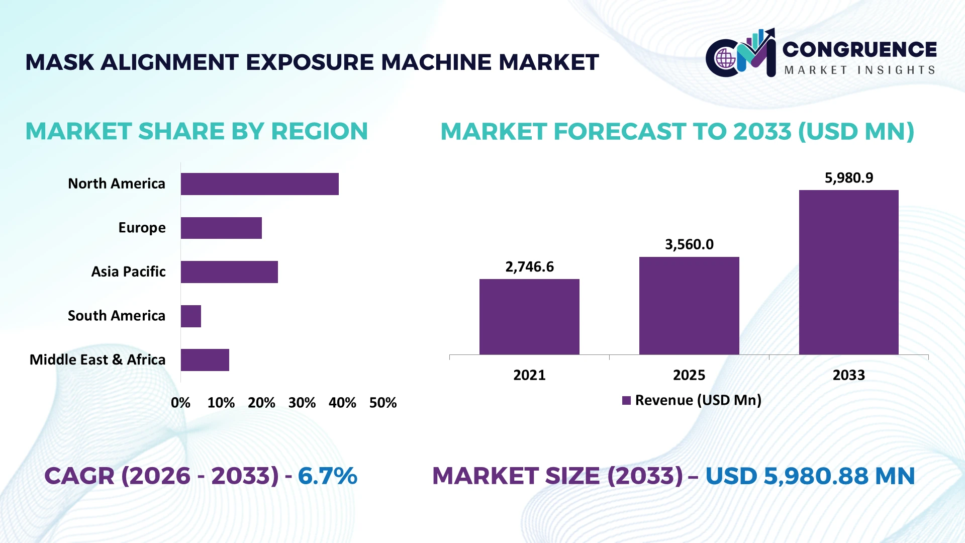
The Global Mask Alignment Exposure Machine Market was valued at USD 3560 Million in 2025 and is anticipated to reach a value of USD 5980.88 Million by 2033 expanding at a CAGR of 6.7% between 2026 and 2033. Growth is driven by 300 mm fab expansion, advanced packaging, MEMS, power semiconductor production, sub-micron overlay requirements, and increasing automation of contact and proximity lithography workflows.
China represents the strongest geographic demand center, accounting for roughly 27% of projected global 300 mm fab-equipment spending in 2026, based on USD 36 billion against USD 133 billion worldwide. Its mainstream 22–40 nm capacity share is projected to reach 42% by 2028, supporting mask-aligner deployment across MEMS, power devices, sensors and packaging. Korea, by comparison, is positioned near USD 27 billion in fab-equipment investment. U.S. semiconductor export controls affecting equipment shipments to China are accelerating localization, supplier diversification and qualification of domestic lithography platforms.
Strategically, equipment suppliers with 300 mm automation, sub-micron alignment and flexible advanced-packaging capability are positioned to capture the highest-value production programs.
Market Size & Growth: USD 3.56 billion in 2025 advances toward USD 5.98 billion by 2033 at 6.7%, supported by advanced packaging, MEMS and automated lithography adoption.
Top Growth Drivers: 300 mm equipment investment rises 18% in 2026, memory investment increases 29%, while China’s mainstream-node capacity share approaches 42% by 2028.
Short-Term Forecast: By 2026, wafer-fab equipment activity rises 10.2%, increasing installation opportunities for alignment, coating and exposure systems supporting technology migrations.
Emerging Technologies: Automated 300 mm handling, 0.5 µm top-side alignment and digital maskless exposure are redefining precision lithography for heterogeneous integration.
Regional Leaders: China targets USD 36 billion, Korea USD 27 billion and Taiwan USD 24.5 billion in 2026 fab-equipment spending, reinforcing Asia’s high-volume lithography concentration.
Consumer/End-User Trends: Asia generated around 70% of SUSS Advanced Backend Solutions sales in 2025, reflecting concentrated adoption among packaging, MEMS and semiconductor manufacturers.
Pilot/Case Example: In May 2025, EV Group introduced LITHOSCALE XT with up to six exposure heads and 5× higher throughput than its previous benchmark system.
Competitive Landscape: SUSS estimates approximately 50% share within its mask-aligner imaging market; EV Group, Canon, Nikon and SMEE remain important global competitors.
Regulatory & ESG Impact: U.S. Section 232 semiconductor actions and a 25% tariff on selected advanced computing chips intensify localization and resilient equipment sourcing strategies.
Investment & Funding: Global 300 mm fab-equipment investment totals approximately USD 439 billion across 2026–2028, strengthening capital deployment toward AI, advanced logic and memory capacity.
Innovation & Future Outlook: Next-generation platforms combine 300 mm automation, digital distortion compensation, dual-wavelength exposure and sub-micron overlay, shifting competition toward software-controlled, high-throughput lithography.
Mask alignment exposure machines are increasingly deployed in advanced packaging, MEMS, power semiconductors, sensors and compound-device fabrication, where precise overlay and thick-resist processing are critical. New 300 mm automated platforms deliver alignment accuracy down to 0.5 µm, while maskless systems are pushing throughput up to fivefold. Export-control pressures are simultaneously accelerating localized equipment qualification, setting the stage for deeper strategic analysis.
Mask alignment exposure equipment is becoming strategically important as semiconductor manufacturers extend lithography investment beyond front-end logic into advanced packaging, MEMS, power devices and heterogeneous integration. Worldwide 300 mm fab-equipment spending is projected to increase 18% in 2026 and 14% in 2027, creating a broader installed base for precision patterning. Supply-chain regionalization is reinforcing this shift as China, Korea, Taiwan and the United States expand domestic fabrication ecosystems.
Technology competition is simultaneously shifting from conventional fixed-mask workflows toward automated alignment and digital exposure. SUSS MA300 Gen3 supports 200–300 mm wafers with top-side alignment accuracy down to 0.5 µm, while EV Group’s six-head LITHOSCALE XT delivers up to five times the throughput of its previous-generation platform. China held approximately 23% of global 300 mm capacity in 2025 versus Korea’s 24%, while Taiwan remained near 21%, highlighting different combinations of manufacturing scale and technology specialization.
Through 2028, advanced-memory, packaging and power-device programs will intensify equipment qualification. A practical example is maskless patterning of warped fan-out wafers, where real-time die-shift compensation supports yield without sacrificing throughput. Equipment companies are therefore prioritizing 300 mm automation, flexible substrate processing and digital lithography partnerships. Competitive advantage will increasingly depend on overlay precision, throughput and application flexibility rather than exposure capability alone.
AI infrastructure, HBM production and heterogeneous integration are increasing requirements for high-precision lithography across packaging and specialty-device lines. Global 300 mm equipment spending is projected to rise 18% in 2026, while memory-equipment investment increases 29%; DRAM equipment spending also rises 29% as manufacturers expand HBM and DDR5 capability. This capacity cycle directly increases requirements for automated wafer handling, thick-resist exposure and accurate overlay. Korea’s memory manufacturers are accelerating technology upgrades, while Chinese fabs continue capacity localization amid semiconductor supply-chain restructuring. Equipment vendors are responding with automated 300 mm mask aligners, dual-wavelength exposure and advanced alignment software. The strategic advantage lies in packaging compatibility: suppliers able to process TSV, RDL and bumping structures on one platform reduce tool fragmentation and improve fab utilization.
Export controls and equipment qualification requirements are fragmenting procurement strategies, particularly for fabs operating in China. U.S. controls introduced in December 2024 covered 24 semiconductor-manufacturing equipment categories and added 140 entities to the Entity List; subsequent policy changes removed license-free treatment previously available to selected foreign-owned fabs in China. Meanwhile, China’s fab-equipment spending was projected to decline 24% in 2025 and another 5% in 2026 after exceptionally high investment. These restrictions complicate sourcing, service availability and production-line qualification, raising switching costs for manufacturers dependent on established process recipes. Suppliers and fabs are responding through localized service networks, alternative component qualification and multi-vendor sourcing. The operational constraint is therefore not simply equipment availability; requalifying lithography processes without sacrificing overlay stability or yield can delay capacity utilization.
Maskless exposure creates a high-value adjacent opportunity where advanced packaging requires rapidly changing layouts, large interposers and compensation for wafer distortion. EV Group’s LITHOSCALE XT uses as many as six exposure heads and delivers up to fivefold higher throughput than its preceding benchmark platform while supporting 300 mm wafers and 300 × 300 mm panels. The system also reaches sub-2-micron lines and spaces, enabling digital patterning for fan-out packaging, MEMS and advanced imaging. This matters because eliminating physical-mask changes improves economics for multi-die designs and frequent product transitions. Taiwan’s continuing 2 nm and sub-2 nm manufacturing expansion strengthens downstream demand for sophisticated packaging ecosystems. Vendors are consequently investing in digital exposure, distortion compensation and panel-compatible architectures. Hybrid portfolios combining mask alignment with maskless lithography offer a differentiated pathway into high-mix advanced-packaging production.
The long-term challenge is maintaining overlay, yield and throughput as packaging architectures become larger, thicker and less geometrically stable. Advanced fan-out substrates can bow or shift during processing, while interposers exceeding conventional reticle dimensions create stitching and alignment complications. EV Group addresses these pressures with real-time distortion and die-shift compensation, while SUSS systems deliver top-side alignment accuracy down to 0.5 µm. Scaling these capabilities across high-volume fabs becomes harder as memory capacity reaches approximately 4.1 million 300 mm wafers monthly in 2026 and 4.2 million in 2027. Manufacturers must synchronize metrology, material handling, alignment software and exposure recipes rather than optimize individual tools independently. Equipment suppliers therefore need deeper process-development partnerships and stronger automation integration; consistent production yield will become a more decisive competitive metric than standalone resolution specifications.
300 mm Automation Reshapes Workflows. Automated loading, recipe management, robotic wafer transfer, and machine-vision alignment are becoming standard on high-volume lithography lines. Global 300 mm installed capacity is projected to increase about 7% in 2026, while related front-end equipment spending rises 25%. Suppliers are prioritizing automated 200–300 mm platforms to reduce manual handling, stabilize overlay performance, and increase utilization across specialty semiconductor and packaging fabs.
Digital Exposure Moves Into HVM. Maskless lithography is shifting from development environments toward high-volume heterogeneous integration. EV Group’s 2025 LITHOSCALE XT uses up to six exposure heads, supports 300 mm wafers and 300 × 300 mm panels, and delivers up to five times higher throughput than its preceding platform. Manufacturers are adopting digital patterning to accelerate layout changes, compensate die shift, and eliminate repeated physical-mask changes.
Mature-Node Utilization Tightens Capacity. AI-related power IC demand is redirecting 8-inch and 12-inch mature-node production. Average utilization among the top ten 8-inch foundries reached about 88% in 2026 and is expected to approach 90% during the second half. Lithography suppliers are strengthening support for power devices, analog ICs, sensors, and specialty wafers as fabs restructure limited capacity toward higher-margin processes.
Localized Support Gains Strategic Weight. China is projected to hold about 25% of global 300 mm front-end capacity in 2026, compared with approximately 23% for Korea and 21% for Taiwan. Export-control pressure is increasing the value of localized qualification, spare-parts availability, and application engineering. Equipment vendors are expanding service capabilities and multi-vendor compatibility because uptime and process support increasingly influence purchasing decisions alongside optical specifications.
Automatic Systems lead the Mask Alignment Exposure Machine Market with an estimated 45% share in 2025, reflecting their strong suitability for high-volume semiconductor, MEMS, and advanced-device manufacturing. These systems integrate automated wafer loading, programmable exposure recipes, machine-vision alignment, and robotic handling, enabling fabs to improve repeatability while reducing operator-dependent variation. Their dominance is reinforced by migration toward 200 mm and 300 mm production environments, where equipment utilization and process consistency directly affect yield. Semi-Automatic Systems represent approximately 25% of demand and remain attractive for specialty fabs requiring lower capital intensity with partial automation.
Multi-Axis Systems are the fastest-growing type, holding an estimated 17% share as heterogeneous packaging, double-sided processing, and complex substrate geometries require more flexible positioning and alignment. Manual Systems account for roughly 13%, concentrated in laboratories, universities, pilot lines, and low-volume specialty fabrication. Suppliers are prioritizing modular automation, higher-axis motion control, recipe digitization, and upgradeable handling systems. Investment is therefore shifting toward platforms that can scale from engineering qualification into sustained production without requiring complete equipment replacement.
Wafer Exposure represents the leading application with an estimated 31% share in 2025, supported by its central role across specialty semiconductors, MEMS, power devices, sensors, and compound-semiconductor fabrication. Demand is concentrated around systems capable of stable proximity or contact exposure, thick-resist processing, and repeatable alignment on increasingly diverse wafer formats. Mask Alignment accounts for approximately 23%, reflecting tighter overlay requirements across multilayer processing, while Patterning contributes about 16% as manufacturers extend lithography into structured resist and microfabrication workflows.
Packaging is the fastest-growing application, representing approximately 19% of demand as redistribution layers, bumping, fan-out packaging, interposers, and heterogeneous integration increase lithography intensity after front-end wafer fabrication. MEMS Fabrication holds around 11%, supported by sensor, automotive, industrial, and medical-device production. Equipment companies are responding through backside alignment, distortion compensation, thick-resist exposure, and flexible substrate handling. The strategic shift is toward multi-application platforms that increase equipment utilization by supporting several lithography steps rather than dedicating one system to a narrow process window.
Semiconductor Manufacturers hold the largest end-user position with an estimated 33% share in 2025, driven by continuous lithography requirements across analog, power, compound-semiconductor, sensor, and specialty-device production. Their larger installed manufacturing base supports demand for automated systems with standardized recipes, high uptime, integrated wafer handling, and repeatable overlay control. Foundries represent approximately 27% and form the fastest-growing buyer group as contract manufacturers expand process portfolios and allocate more capacity toward AI-related, power, mature-node, and specialty applications.
Device Manufacturers account for roughly 18%, especially where integrated sensor, optoelectronic, and power-device companies maintain internal fabrication. MEMS Manufacturers represent approximately 14%, emphasizing double-sided alignment, thick-resist compatibility, and non-standard substrate processing, while Research Institutes account for around 8% and prioritize configurable systems for process development. Suppliers are targeting foundries through scalable automation, application-specific process modules, and stronger service ecosystems. Competitive positioning increasingly depends on enabling one platform to support multiple customer products, shortening qualification cycles and improving overall tool utilization.
Asia-Pacific accounted for the largest market share at 67% in 2025 however, North America is expected to register the fastest growth, expanding at a CAGR of 8.1% between 2026 and 2033.
Domestic Fab Expansion Accelerates Equipment Localization
North America accounted for an estimated 12% of the Mask Alignment Exposure Machine Market in 2025, with the United States concentrating demand across advanced packaging, MEMS, compound semiconductors, power electronics, photonics and research fabs. The Americas are positioned near 9% of worldwide 300 mm front-end capacity, while 300 mm equipment investment is accelerating as domestic fabs move from construction into tool installation and qualification. Four new semiconductor fab projects began construction across the Americas in 2025, strengthening requirements for lithography, wafer handling and process-control infrastructure. Federal semiconductor policy and supply-chain localization are also pushing manufacturers toward domestic engineering support and resilient equipment sourcing. Mask-aligner vendors are consequently emphasizing automated substrate handling, sub-micron overlay, localized service and compatibility with specialty processes rather than competing solely on exposure resolution.
United States Market Outlook: Arizona, Texas, New York and Oregon form an expanding semiconductor manufacturing corridor spanning foundry, memory, analog, power and advanced-packaging operations. U.S. manufacturing incentives are accelerating equipment qualification while domestic suppliers and international OEMs strengthen application-engineering capacity. The Americas are expected to represent roughly 9% of worldwide 300 mm capacity, providing a larger addressable installed base for precision lithography systems.
Specialty Semiconductor Capacity Drives Modernization
Europe represented an estimated 10% of global mask alignment exposure machine demand in 2025, supported by automotive semiconductors, MEMS, power electronics, analog devices, silicon carbide and photonics. Germany, France, Italy and Austria are converting semiconductor sovereignty policies into new manufacturing infrastructure, creating opportunities for contact and proximity lithography alongside advanced process equipment. European Chips Act initiatives include 13 approved state-aid decisions covering semiconductor facilities, while new projects span 300 mm FD-SOI, FinFET, SiC, mixed-signal devices and advanced packaging. This diversified technology mix favors flexible aligners capable of processing thick resists, unconventional substrates and double-sided structures. Equipment suppliers are aligning product development with automotive-grade process control, energy-efficient manufacturing and stronger local technical support. Europe’s advantage lies less in sheer wafer volume and more in high-value specialty processes where mask alignment remains technically and economically competitive.
Germany Market Outlook: Dresden is emerging as Europe’s most consequential semiconductor production cluster. ESMC’s planned 300 mm facility targets 480,000 wafers annually at full capacity by 2029, complementing Infineon, Bosch and GlobalFoundries operations. The concentration of automotive, industrial and mixed-signal manufacturing strengthens demand for lithography systems supporting 12–28 nm peripheral processes, MEMS, power devices and heterogeneous integration.
Manufacturing Scale Sustains Lithography Leadership
Asia-Pacific commanded an estimated 67% market share in 2025, reflecting unmatched concentration of wafer fabrication, outsourced semiconductor manufacturing, MEMS production and advanced packaging. China, Korea, Taiwan and Japan collectively dominate 300 mm capacity, with China alone projected to reach 25% of worldwide capacity in 2026, followed by Korea at 23%, Taiwan at 21% and Japan at 12%. This manufacturing density creates continuous demand for automated alignment, proximity exposure and specialty lithography across mature-node ICs, power devices, sensors and packaging. Export controls are simultaneously accelerating equipment localization in China, while Taiwan and Korea emphasize advanced foundry and memory ecosystems. Vendors are responding through application centers, localized service teams and production-grade automation. A non-obvious advantage is installed-base proximity: dense semiconductor clusters shorten qualification cycles because equipment makers can support multiple fabs through concentrated engineering networks.
China Market Outlook: China is strategically significant because mature-node localization is occurring alongside rapid domestic equipment qualification. Its 300 mm capacity is positioned around 2.4 million wafers per month in 2026, providing substantial demand for lithography outside leading-edge EUV processes. Power semiconductors, MEMS, analog devices and advanced packaging are particularly relevant for domestic mask-aligner manufacturers competing on localization, service responsiveness and procurement security.
Policy Support Rebuilds Semiconductor Capability
South America held an estimated 3% share in 2025, with demand concentrated in university cleanrooms, semiconductor assembly, microelectronics R&D, sensors and selected device-production facilities. Brazil provides the region’s strongest industrial foundation and is rebuilding semiconductor capability through Brasil Semicon, PADIS and targeted development financing. Policy now supports chip design, physical processing, R&D and manufacturing infrastructure, improving conditions for laboratory and pilot-scale lithography equipment deployment. The market nevertheless remains constrained by limited wafer-fabrication scale, imported equipment dependence and a smaller specialist workforce than established semiconductor hubs. Suppliers therefore compete through compact manual and semi-automatic systems, technical partnerships and research-focused configurations rather than high-volume automated installations. Increasing public support for microelectronics creates a pathway from academic lithography toward commercial specialty-device manufacturing, but equipment utilization remains the critical economic threshold for expansion.
Brazil Market Outlook: Brazil anchors regional semiconductor development through production incentives, R&D infrastructure and industrial modernization. The government invested R$267 million in strategic ICT projects during 2025, 116% above 2024 support, while more than R$1.2 billion is planned through FNDCT for semiconductors in 2026. This funding strengthens laboratories, pilot manufacturing and equipment modernization, supporting selective mask-aligner procurement.
Semiconductor Localization Moves Into Infrastructure Building
Middle East & Africa represented an estimated 8% of market demand in 2025, although commercial installations remain concentrated in Israel, the Gulf states and South Africa rather than broadly distributed. Israel contributes established semiconductor fabrication and advanced R&D capability, while Saudi Arabia and the UAE are building semiconductor design, AI and advanced-manufacturing ecosystems through sovereign investment and international partnerships. The wider Europe-and-Middle-East manufacturing grouping is projected near 7% of worldwide 300 mm front-end capacity, illustrating a modest but strategically relevant production base. Current mask-aligner opportunities are strongest in research centers, compound semiconductors, MEMS, photonics and pilot manufacturing rather than large-scale commodity wafer production. Vendors are positioning through university partnerships, process-development support and configurable lithography platforms. The decisive constraint remains ecosystem depth: cleanroom infrastructure, process engineers and downstream packaging capability must expand together before high-volume equipment deployment becomes economical.
Israel Market Outlook: Israel remains the region’s most mature semiconductor operating environment, supported by established fabrication, multinational R&D centers and a dense chip-design ecosystem. Its advantage is process sophistication rather than regional production volume, supporting demand for research and specialty lithography in MEMS, sensors, photonics and advanced-device development where configurable alignment systems provide greater process flexibility than high-cost projection tools.
SUSS MicroTec and EV Group compete directly for high-precision automated mask-alignment installations, while Canon targets broader lithography workflows and MIDAS System, Neutronix Quintel and OAI compete strongly in research, MEMS and specialty-device environments. The top five suppliers are estimated to control approximately 68% of market demand, creating a moderately concentrated structure. Technology increasingly outweighs basic tool pricing: automated platforms command roughly 45% of type demand, while systems supporting 300 mm substrates address the fastest modernization programs. Sub-micron alignment approaching 0.5 µm gives premium suppliers a process-control advantage over conventional manual architectures. Competition is shifting toward automation, backside alignment, thick-resist processing, integrated metrology and application-specific customization. SUSS and EV Group are extending modular platforms, software control and global service capability, while smaller suppliers defend positions through lower ownership costs and flexible configurations. Qualification time, installed-base support and process know-how remain substantial entry barriers. Winning requires precision, application breadth, dependable service and scalable automation.
SUSS MicroTec
EV Group
Canon Inc.
MIDAS System Co., Ltd.
Neutronix Quintel
Optical Associates, Inc. (OAI)
Shanghai Micro Electronics Equipment (SMEE)
ABM, Inc.
HÜTTINGER Elektronik / specialized lithography equipment providers
C&D Semiconductor Services
Kloe
Durham Magneto Optics
SVG / specialty lithography equipment providers
MicroTech Systems
Current mask aligners are shifting toward automated 200–300 mm handling, machine-vision alignment and digitally controlled exposure. SUSS MA300 Gen3 achieves 0.5 µm top-side alignment, while automated recipe control reduces operator-dependent variation by an estimated 10–15% versus manual workflows. Deployment is strongest in advanced packaging, MEMS and power-device fabs, where automation improves repeatability, equipment utilization and multilayer overlay control.
Emerging digital lithography adds real-time distortion correction, infrared alignment and dual-wavelength exposure. EV Group’s LITHOSCALE XT uses up to six exposure heads and delivers fivefold higher throughput than its previous platform, supporting sub-2 µm patterning on 300 mm wafers. Compared with legacy single-layout mask workflows, digital pattern switching can eliminate 100% of physical mask changes between compatible designs, benefiting high-mix fan-out and heterogeneous-integration manufacturers.
Disruptive integration through maskless exposure, AI-assisted image recognition and connected metrology will reshape equipment selection through 2026–2028. UV-LED retrofits can cut exposure-system electricity consumption by about 81% versus mercury lamps, while predictive process monitoring strengthens uptime. Suppliers combining alignment, exposure, handling and analytics gain the competitive advantage as fabs prioritize flexible platforms that shorten qualification, accommodate warped substrates and support production without sacrificing precision. This convergence reduces tool fragmentation and simplifies process transfer from pilot development into manufacturing.
March 2026 SUSS reported Advanced Backend Solutions, including mask aligners, generated 349.7 million euros in 2025 sales. The scale confirms sustained commercial deployment across packaging lithography, while reinforcing investment capacity for automated alignment platforms. Source: FinancialFilings
May 2025 EV Group introduced LITHOSCALE XT with six parallel exposure heads and fivefold higher throughput than its predecessor. The platform shifts maskless lithography toward high-volume heterogeneous integration, reducing traditional throughput constraints for advanced packaging manufacturers. Source: EEHerald
September 2024 Canon released the FPA-3030i6 i-line system, increasing 200-mm productivity from 123 to 130 wafers hourly while reducing lens aberration over 50%. The upgrade strengthens specialty lithography economics for SiC, GaN and power-device production. Source: Canon
February 2026 University of Waterloo upgraded its SUSS MA6 from mercury-lamp exposure to UV-LED technology, cutting average daily electricity consumption from 7.62 kWh to 1.42 kWh. The retrofit demonstrates lower-energy modernization of installed mask-aligner infrastructure. Source: Waterloo
The Mask Alignment Exposure Machine Market report evaluates Automatic Systems, Manual Systems, Semi-Automatic Systems and Multi-Axis Systems across Wafer Exposure, Mask Alignment, Patterning, MEMS Fabrication and Packaging applications. End-user coverage includes Semiconductor Manufacturers, Device Manufacturers, Foundries, MEMS Manufacturers and Research Institutes. Automatic systems represent an estimated 45% of 2025 demand, highlighting the transition toward production-scale automation, repeatable overlay and integrated wafer handling.
Regional assessment covers North America, Europe, Asia-Pacific, South America, and Middle East & Africa, with Asia-Pacific representing an estimated 67% of deployment value. Technology coverage examines sub-micron alignment, 200–300 mm automation, backside and infrared alignment, thick-resist exposure, UV-LED modernization, maskless lithography and digital distortion compensation. The 2026–2033 framework supports investment planning, geographic expansion, equipment portfolio positioning and competitive benchmarking while identifying emerging opportunities across heterogeneous integration, MEMS, power semiconductors and advanced packaging.
| Report Attribute/Metric | Report Details |
|---|---|
Market Revenue in 2025 | USD 3560 Million |
Market Revenue in 2033 | USD 5980.88 Million |
CAGR (2026 - 2033) | 6.7% |
Base Year | 2025 |
Forecast Period | 2026 - 2033 |
Historic Period | 2021 - 2025 |
Segments Covered | By Type
By Application
By End-User
|
Key Report Deliverable | Revenue Forecast, Growth Trends, Market Dynamics, Segmental Overview, Regional and Country-wise Analysis, Competition Landscape |
Region Covered | North America, Europe, Asia-Pacific, South America, Middle East, Africa |
Key Players Analyzed | SUSS MicroTec, EV Group, Canon Inc., MIDAS System Co., Ltd., Neutronix Quintel, Optical Associates, Inc. (OAI), Shanghai Micro Electronics Equipment (SMEE), ABM, Inc., HÜTTINGER Elektronik / specialized lithography equipment providers, C&D Semiconductor Services, Kloe, Durham Magneto Optics, SVG / specialty lithography equipment providers, MicroTech Systems |
Customization & Pricing | Available on Request (10% Customization is Free) |