
Reports
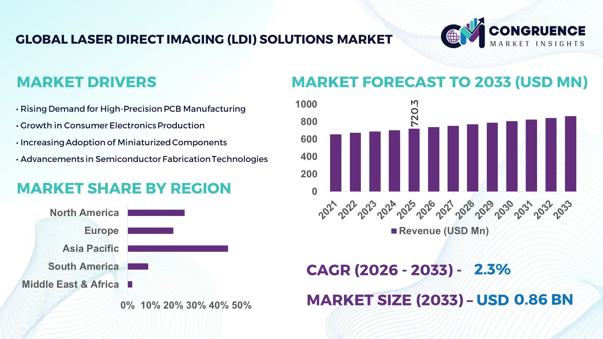
The Global Laser Direct Imaging (LDI) Solutions Market was valued at USD 720.32 Million in 2025 and is anticipated to reach a value of USD 864.04 Million by 2033 expanding at a CAGR of 2.3% between 2026 and 2033. This steady expansion is primarily driven by the increasing demand for high-precision printed circuit board (PCB) manufacturing across advanced electronics and semiconductor industries.
China stands as the dominant country in the Laser Direct Imaging (LDI) Solutions market, supported by extensive PCB manufacturing capacity and continuous investment in electronics infrastructure. The country produces over 50% of the global PCB output, with more than 2,500 registered PCB manufacturers operating across industrial hubs such as Guangdong and Jiangsu. Investment in high-end manufacturing equipment, including LDI systems, exceeded USD 3 billion in recent years, reflecting a strong push toward automation and miniaturization. Additionally, adoption of LDI technology in China’s flexible and high-density interconnect (HDI) PCB segments has surpassed 65%, driven by demand from consumer electronics, automotive electronics, and 5G communication devices. Continuous advancements in laser resolution capabilities, reaching sub-10 micron precision, further reinforce the country's technological leadership in this market.
Market Size & Growth: Valued at USD 720.32 Million in 2025, projected to reach USD 864.04 Million by 2033, growing at 2.3% CAGR due to increasing demand for precision PCB fabrication.
Top Growth Drivers: 68% rise in HDI PCB adoption, 55% improvement in production efficiency, 48% increase in demand for miniaturized electronics.
Short-Term Forecast: By 2028, manufacturing defect rates are expected to reduce by 30% due to advanced imaging automation.
Emerging Technologies: Integration of AI-based imaging calibration, UV laser advancements, and digital lithography systems.
Regional Leaders: Asia-Pacific projected at USD 420 Million by 2033 with strong electronics manufacturing; North America at USD 190 Million driven by aerospace electronics; Europe at USD 160 Million with automotive electronics expansion.
Consumer/End-User Trends: Increased adoption among PCB manufacturers, semiconductor fabs, and automotive electronics producers focusing on precision and yield optimization.
Pilot or Case Example: In 2024, a leading PCB manufacturer achieved 28% production efficiency improvement using automated LDI systems.
Competitive Landscape: Market leader holds approximately 22% share, followed by Orbotech, SCREEN Holdings, Manz AG, and Via Mechanics.
Regulatory & ESG Impact: Environmental policies promoting chemical-free imaging processes are accelerating LDI adoption.
Investment & Funding Patterns: Over USD 1.2 billion invested in advanced PCB manufacturing technologies globally in recent years.
Innovation & Future Outlook: Increased integration with Industry 4.0 systems and real-time process monitoring technologies.
The Laser Direct Imaging (LDI) Solutions market is witnessing robust demand across key industry sectors, particularly consumer electronics, automotive electronics, and telecommunications, which collectively contribute over 70% of total demand. Innovations such as high-speed UV laser systems and AI-driven alignment technologies are enhancing throughput and reducing defect rates. Regulatory pressure to minimize chemical usage in traditional photolithography is further accelerating LDI adoption due to its environmentally friendly, maskless process. Asia-Pacific leads consumption due to high-volume electronics manufacturing, while Europe shows steady growth driven by electric vehicle electronics. The market is also benefiting from increased investments in smart manufacturing, with future trends focusing on ultra-fine line imaging and integration with automated inspection systems for improved production reliability.
The Laser Direct Imaging (LDI) Solutions market holds significant strategic importance in enabling next-generation electronics manufacturing, particularly in high-density interconnect (HDI) and flexible PCB production. As global electronics demand continues to evolve toward miniaturization and higher functionality, LDI systems provide critical advantages in precision, repeatability, and process efficiency. Advanced UV laser imaging delivers up to 40% improvement in pattern accuracy compared to conventional photolithography methods, making it a preferred technology for manufacturers aiming to enhance yield and reduce defects.
Asia-Pacific dominates in production volume due to its extensive electronics manufacturing ecosystem, while North America leads in technology adoption, with over 60% of advanced PCB facilities integrating digital imaging solutions. By 2028, AI-powered process optimization in LDI systems is expected to reduce production errors by up to 35%, significantly improving operational efficiency and cost control. Companies are also aligning with sustainability goals, committing to reduce chemical waste by 50% through the adoption of maskless imaging technologies by 2030.
A notable micro-scenario includes a 2025 deployment in South Korea, where a semiconductor supplier achieved a 25% increase in throughput and a 20% reduction in rework rates using AI-integrated LDI platforms. This reflects the growing importance of intelligent automation in the sector. The Laser Direct Imaging (LDI) Solutions market is positioned as a critical pillar for resilient manufacturing, enabling compliance with environmental regulations while supporting scalable, high-precision production. Its future pathways are closely tied to digital transformation, sustainability, and the ongoing evolution of advanced electronics ecosystems.
The increasing demand for HDI PCBs is a major growth driver for the Laser Direct Imaging (LDI) Solutions market, as these advanced circuit boards require extremely fine line widths and precise alignment. HDI PCBs are widely used in smartphones, wearable devices, and automotive electronics, where compact design and high performance are essential. LDI systems enable imaging resolutions below 10 microns, which is critical for producing multilayer boards with complex circuitry. Global smartphone shipments exceeding 1.2 billion units annually and the rapid expansion of electric vehicle electronics have significantly boosted HDI PCB production. Furthermore, LDI technology improves manufacturing yield by up to 25% compared to traditional exposure methods, making it a preferred solution for high-volume production environments.
High capital expenditure associated with Laser Direct Imaging (LDI) systems remains a significant restraint for market expansion, particularly among small and medium-sized manufacturers. Advanced LDI equipment can cost substantially more than conventional photolithography systems, requiring significant upfront investment in machinery, software integration, and skilled workforce training. Additionally, maintenance and calibration costs add to the operational burden. Many manufacturers operating in cost-sensitive regions continue to rely on traditional exposure methods due to lower initial costs, despite lower efficiency. The complexity of integrating LDI systems into existing production lines also creates barriers, as it may require infrastructure upgrades and process redesign, limiting widespread adoption in certain segments of the market.
The rapid expansion of advanced electronics manufacturing presents substantial opportunities for the Laser Direct Imaging (LDI) Solutions market. Emerging technologies such as 5G infrastructure, Internet of Things (IoT) devices, and electric vehicles are driving demand for highly sophisticated PCBs with increased functionality and compact designs. LDI systems are well-suited for these applications due to their ability to deliver precise imaging without the need for physical masks. The global rollout of 5G networks alone has led to a surge in demand for high-frequency PCBs, where LDI technology improves signal integrity and manufacturing accuracy. Additionally, increasing investments in semiconductor fabrication and smart manufacturing facilities are creating new avenues for LDI adoption, particularly in regions focusing on technological self-sufficiency and supply chain resilience.
Rapid technological evolution within the Laser Direct Imaging (LDI) Solutions market presents a significant challenge, particularly in terms of workforce readiness and system adaptability. As LDI systems become more advanced, incorporating AI-driven alignment and real-time process monitoring, the need for highly skilled operators and engineers increases. However, there is a noticeable shortage of professionals with expertise in laser imaging technologies and digital manufacturing systems. This skill gap can lead to suboptimal system utilization and reduced return on investment. Additionally, frequent technological upgrades require continuous investment in training and equipment modernization, placing financial pressure on manufacturers. Compatibility issues between legacy systems and new LDI technologies further complicate implementation, slowing down adoption rates in certain regions.
• Increasing Adoption of AI-Driven Imaging Optimization: The integration of artificial intelligence into Laser Direct Imaging (LDI) systems is significantly improving operational precision and efficiency. Advanced AI-based calibration tools have demonstrated up to 35% improvement in alignment accuracy and a 28% reduction in imaging defects across high-density PCB production lines. Over 60% of newly installed LDI systems in 2025 feature AI-enabled process optimization modules, enabling predictive maintenance and automated error correction. This trend is particularly strong in Asia-Pacific, where smart manufacturing adoption has increased by over 50% in leading electronics hubs.
• Expansion of Ultra-Fine Line Imaging Capabilities: Demand for ultra-fine line imaging below 10 microns is accelerating as electronic devices become more compact and complex. Approximately 48% of next-generation PCB designs now require sub-10 micron resolution, compared to just 30% five years ago. LDI solutions equipped with advanced UV laser sources have improved line definition precision by 40%, enabling manufacturers to meet stringent design requirements for 5G modules and wearable electronics. This capability is becoming a key differentiator for suppliers targeting high-performance applications.
• Shift Toward Environmentally Sustainable Manufacturing Processes: Environmental sustainability is reshaping production strategies in the Laser Direct Imaging (LDI) Solutions market, with manufacturers actively replacing traditional photolithography methods. LDI eliminates the need for photomasks and chemical-intensive processes, reducing chemical waste by up to 50% and water consumption by approximately 30%. Over 45% of PCB manufacturers in Europe have transitioned to maskless imaging technologies to comply with stricter environmental regulations, reflecting a broader industry commitment to green manufacturing practices.
• Growth in High-Speed, High-Throughput Production Systems: The need for faster production cycles is driving the development of high-speed LDI systems capable of increasing throughput without compromising precision. Modern LDI machines have achieved throughput improvements of up to 32%, enabling large-scale manufacturers to meet rising demand for consumer electronics and automotive components. Approximately 55% of large PCB fabrication facilities have upgraded to high-throughput LDI platforms, reducing production cycle times by nearly 25%. This trend is particularly prominent in regions with high-volume manufacturing requirements, including China and South Korea.
The Laser Direct Imaging (LDI) Solutions market segmentation is primarily defined by type, application, and end-user industries, each playing a critical role in shaping demand patterns and technological adoption. By type, UV laser-based systems dominate due to their superior precision and compatibility with advanced PCB manufacturing requirements. Application-wise, PCB fabrication remains the primary segment, driven by increasing demand for HDI and flexible circuit boards in modern electronics. From an end-user perspective, consumer electronics manufacturers account for a significant portion of adoption, supported by high production volumes and the need for miniaturized components. Additionally, automotive and telecommunications sectors are witnessing rising integration of LDI systems due to growing demand for advanced electronic modules. Regional consumption trends indicate strong dominance of Asia-Pacific, supported by large-scale manufacturing, while North America and Europe show increasing adoption driven by technological advancements and sustainability requirements.
The Laser Direct Imaging (LDI) Solutions market by type is segmented into UV Laser Direct Imaging systems, Digital Laser Imaging systems, and hybrid imaging solutions. UV Laser Direct Imaging systems lead the segment, accounting for approximately 58% of total adoption due to their ability to achieve sub-10 micron resolution and superior line accuracy. These systems are widely used in HDI PCB production, where precision is critical for multilayer circuit designs. In comparison, Digital Laser Imaging systems hold around 27% share, offering flexibility and faster setup times, making them suitable for small-batch and prototype production. Hybrid imaging solutions, combining traditional and digital techniques, contribute the remaining 15%, catering to niche applications requiring cost-performance balance.
The fastest-growing segment is Digital Laser Imaging systems, expanding at an estimated growth rate of 5.1%, driven by increasing demand for rapid prototyping and flexible manufacturing processes. Their ability to reduce setup time by nearly 40% compared to conventional systems is a key growth factor.
By application, the Laser Direct Imaging (LDI) Solutions market is dominated by PCB manufacturing, which accounts for approximately 65% of total usage due to the widespread adoption of HDI and flexible PCBs in consumer electronics and communication devices. Semiconductor packaging applications follow with around 20% share, benefiting from the need for high-precision imaging in advanced chip designs. However, flexible electronics applications are emerging as the fastest-growing segment, expected to grow at a rate of 6.3%, driven by increasing adoption in wearable devices and foldable displays.
Other applications, including MEMS fabrication and microfluidic device production, collectively contribute about 15% of the market, offering specialized use cases in medical and industrial sectors. The ability of LDI systems to deliver maskless imaging and reduce defect rates by up to 25% makes them highly suitable for these precision-driven applications.
In terms of end-users, the consumer electronics industry leads the Laser Direct Imaging (LDI) Solutions market, accounting for approximately 52% of total demand due to high production volumes of smartphones, tablets, and wearable devices. Automotive electronics represent around 23% of the market, driven by increasing integration of advanced driver-assistance systems (ADAS) and electric vehicle components. Telecommunications follows with approximately 15% share, supported by the rapid deployment of 5G infrastructure and networking equipment.
The fastest-growing end-user segment is automotive electronics, expanding at an estimated rate of 5.6%, fueled by rising adoption of electric vehicles and advanced onboard electronic systems. Automotive manufacturers are increasingly relying on LDI systems to produce high-reliability PCBs capable of operating under extreme conditions. Other end-users, including aerospace, healthcare devices, and industrial automation, collectively account for about 10% of the market, with adoption rates increasing due to demand for precision and reliability.
Region Asia-Pacific accounted for the largest market share at 52% in 2025 however, North America is expected to register the fastest growth, expanding at a CAGR of 4.1% between 2026 and 2033.
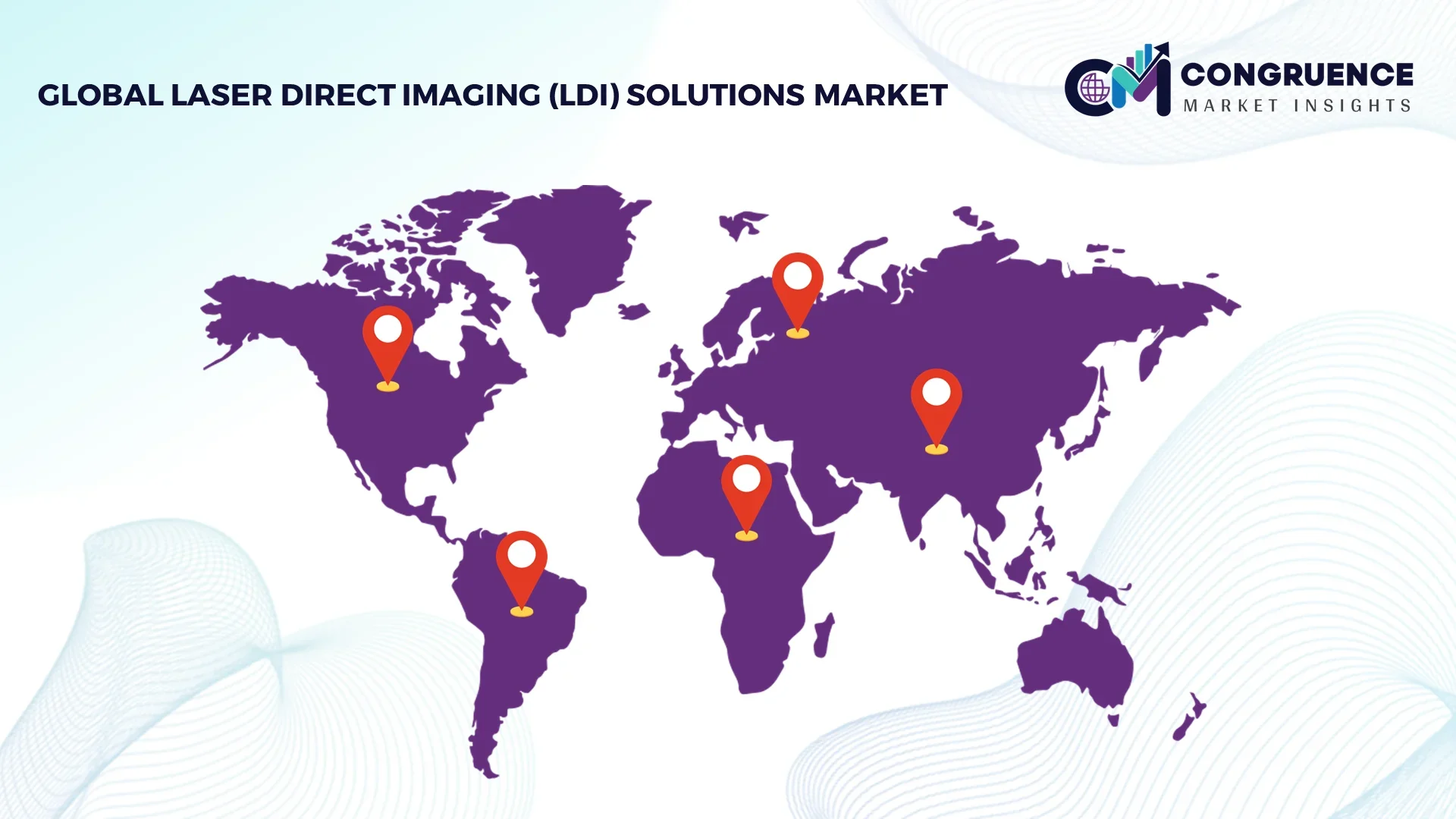
Asia-Pacific’s dominance is supported by its massive PCB production ecosystem, with China, Japan, and South Korea collectively contributing over 70% of global PCB manufacturing output. China alone hosts more than 2,500 PCB production facilities, while Japan leads in high-end substrate innovation with over 35% of advanced packaging output. North America, holding approximately 22% share, is witnessing accelerated adoption of high-precision LDI systems driven by aerospace and defense electronics demand. Europe contributes around 18% of the global market, supported by automotive electronics manufacturing in Germany and France. Meanwhile, South America and the Middle East & Africa collectively account for nearly 8%, with increasing investments in electronics infrastructure and localized manufacturing capabilities. Regional consumption patterns highlight that over 65% of LDI installations are concentrated in high-volume manufacturing zones, while emerging economies are focusing on digital transformation and localized production strategies.
How is advanced electronics manufacturing accelerating precision imaging adoption across industries?
North America holds approximately 22% of the Laser Direct Imaging (LDI) Solutions market, driven by strong demand from aerospace, defense, and high-performance computing sectors. The United States accounts for nearly 80% of regional demand, supported by over 1,200 advanced electronics manufacturing facilities. Regulatory frameworks promoting domestic semiconductor production, including incentives exceeding USD 50 billion, have accelerated investments in advanced PCB and imaging technologies. The region is also witnessing rapid digital transformation, with over 58% of manufacturers integrating Industry 4.0 solutions such as AI-driven process monitoring. Technological advancements include the deployment of high-speed UV laser imaging systems capable of improving throughput by up to 30%. A notable regional player has focused on developing next-generation LDI platforms with enhanced resolution capabilities below 8 microns, targeting aerospace-grade PCB applications. Consumer behavior in this region reflects high enterprise adoption, particularly in healthcare and financial electronics systems, where precision and reliability are critical performance metrics.
What role do sustainability regulations play in shaping high-precision imaging adoption trends?
Europe accounts for approximately 18% of the Laser Direct Imaging (LDI) Solutions market, with Germany, the United Kingdom, and France leading regional demand. Germany alone contributes nearly 35% of Europe’s electronics manufacturing output, particularly in automotive electronics and industrial automation systems. Strict environmental regulations have driven the adoption of LDI solutions, with over 48% of manufacturers transitioning to maskless imaging processes to reduce chemical waste. Sustainability initiatives aligned with carbon neutrality targets have encouraged the adoption of energy-efficient laser systems, reducing energy consumption by up to 20%. Technological advancements include integration of automated inspection systems with LDI platforms, improving defect detection rates by 25%. A regional equipment manufacturer has introduced eco-friendly LDI systems with reduced emissions, targeting automotive electronics suppliers. Consumer behavior in Europe is influenced by regulatory compliance, leading to increased demand for environmentally sustainable and traceable manufacturing processes.
Why is large-scale electronics manufacturing fueling precision imaging innovation at unprecedented levels?
Asia-Pacific leads the Laser Direct Imaging (LDI) Solutions market in both volume and adoption, contributing over 52% of global demand. China, Japan, and South Korea are the top consuming countries, collectively accounting for more than 70% of regional usage. China’s electronics manufacturing infrastructure includes over 2,500 PCB factories, while Japan leads in advanced semiconductor packaging technologies. India is emerging as a growing market, with electronics manufacturing output increasing by over 25% in recent years. The region is characterized by rapid infrastructure expansion and high-volume production, with more than 65% of global LDI system installations concentrated in this region. Innovation hubs in South Korea and Taiwan are driving advancements in ultra-fine imaging, achieving resolutions below 10 microns. A leading regional manufacturer has deployed AI-integrated LDI systems, improving production efficiency by 28%. Consumer behavior in Asia-Pacific is driven by strong demand for smartphones, wearable devices, and 5G infrastructure, contributing to sustained growth in high-precision PCB manufacturing.
How are emerging electronics manufacturing initiatives shaping precision imaging demand across industries?
South America represents approximately 5% of the Laser Direct Imaging (LDI) Solutions market, with Brazil and Argentina as key contributors. Brazil accounts for nearly 60% of regional electronics production, supported by over 300 manufacturing facilities focusing on consumer electronics and automotive components. Infrastructure development and energy sector investments have increased demand for reliable electronic systems, indirectly boosting the adoption of advanced imaging technologies. Government incentives promoting local manufacturing and import substitution policies have encouraged investment in advanced production equipment, including LDI systems. Adoption of digital manufacturing technologies has increased by over 20% across key industrial sectors. A regional electronics manufacturer has implemented LDI solutions to improve PCB production accuracy, achieving a 22% reduction in defects. Consumer behavior in South America is influenced by growing demand for localized production and language-specific electronic interfaces, supporting gradual market expansion.
What factors are driving modernization of precision electronics manufacturing capabilities in developing economies?
The Middle East & Africa region holds approximately 3% of the Laser Direct Imaging (LDI) Solutions market, with the UAE and South Africa leading adoption. The UAE accounts for nearly 40% of regional demand, driven by investments in smart infrastructure and advanced technology projects. South Africa contributes around 30%, supported by industrial automation initiatives and electronics manufacturing growth. Demand trends are influenced by sectors such as oil and gas, construction, and telecommunications, where reliable electronic systems are critical. Technological modernization efforts have increased adoption of automated manufacturing solutions by over 18% in recent years. Trade partnerships and government-led digital transformation programs have further accelerated market development. A regional technology firm has introduced LDI-enabled PCB production systems, improving efficiency by 20% in local manufacturing units. Consumer behavior reflects increasing demand for high-quality electronic devices and infrastructure-driven solutions.
China – 38% market share in the Laser Direct Imaging (LDI) Solutions market, driven by extensive PCB manufacturing capacity and strong electronics production ecosystem.
United States – 21% market share in the Laser Direct Imaging (LDI) Solutions market, supported by advanced aerospace, defense, and semiconductor industries.
The Laser Direct Imaging (LDI) Solutions market exhibits a moderately consolidated competitive structure, with approximately 25–30 active global and regional players competing across different technology segments. The top five companies collectively account for nearly 58% of the total market share, reflecting strong technological capabilities and established customer relationships. Market leaders differentiate themselves through continuous innovation, particularly in high-resolution imaging systems and AI-integrated process optimization solutions.
Strategic initiatives such as partnerships, mergers, and product launches play a crucial role in shaping the competitive landscape. Over 40% of leading companies have introduced next-generation LDI systems with sub-10 micron resolution capabilities in the past three years. Additionally, collaborations with semiconductor manufacturers and PCB producers have increased by 35%, enabling companies to expand their application portfolios.
Innovation trends include the integration of Industry 4.0 technologies, with more than 50% of major players investing in smart manufacturing solutions. Companies are also focusing on sustainability, developing eco-friendly systems that reduce chemical usage by up to 50%. The competitive environment is further intensified by regional players offering cost-effective solutions, particularly in Asia-Pacific, where production scale and pricing strategies play a significant role.
Orbotech Ltd.
SCREEN Holdings Co., Ltd.
Manz AG
Via Mechanics Ltd.
Limata GmbH
Hitachi High-Tech Corporation
ORC Manufacturing Co., Ltd.
Aiscent Technologies Co., Ltd.
CFMEE
Technological advancements in the Laser Direct Imaging (LDI) Solutions market are centered around improving imaging precision, throughput efficiency, and process automation to meet the evolving demands of high-density electronics manufacturing. Modern LDI systems utilize ultraviolet (UV) laser wavelengths, typically in the range of 355 nm, enabling resolution capabilities below 10 microns, which is essential for high-density interconnect (HDI) and flexible printed circuit boards (PCBs). Recent innovations have further pushed imaging precision to nearly 5 microns, supporting next-generation semiconductor packaging and microelectronics fabrication.
Artificial intelligence and machine learning integration have become critical in optimizing imaging processes. AI-driven alignment systems can improve registration accuracy by up to 35% while reducing setup time by approximately 25%. Predictive maintenance algorithms are also being deployed, decreasing unexpected equipment downtime by nearly 20% and enhancing overall operational efficiency. Additionally, digital twin technology is being introduced in advanced manufacturing facilities, enabling real-time simulation and process optimization, which can improve yield rates by up to 18%.
Another key technological trend is the development of high-speed multi-beam laser systems, which significantly enhance throughput. These systems can increase production speed by over 30% compared to traditional single-beam configurations, allowing manufacturers to scale operations without compromising accuracy. Integration with automated optical inspection (AOI) systems is also becoming standard, enabling inline defect detection and reducing defect rates by up to 28%.
Sustainability-focused innovations are gaining traction, with LDI systems eliminating the need for photomasks and reducing chemical usage by approximately 50%. Water consumption in PCB fabrication processes has also decreased by nearly 30% with the adoption of maskless imaging technologies. Furthermore, advancements in software-driven patterning and real-time data analytics are enabling manufacturers to achieve higher process repeatability and consistency, making LDI solutions a cornerstone technology in smart manufacturing environments.
• In March 2025, SCREEN Holdings Co., Ltd. introduced an upgraded LDI system featuring enhanced multi-beam laser architecture capable of improving throughput by approximately 25% while maintaining sub-10 micron accuracy. The system is designed for high-volume PCB manufacturing and integrates advanced process automation features. Source: www.screen.co.jp
• In October 2024, Manz AG expanded its electronics manufacturing portfolio by launching a next-generation digital LDI platform focused on flexible PCB production. The system demonstrated a 30% reduction in production cycle time and improved alignment precision for complex circuit designs. Source: www.manz.com
• In July 2024, Han’s Laser Technology Industry Group Co., Ltd. deployed an advanced UV LDI system in its PCB solutions segment, achieving a 20% increase in production efficiency and supporting ultra-fine line imaging below 8 microns for high-end electronics applications. Source: www.hanslaser.com
• In January 2025, Hitachi High-Tech Corporation introduced a new laser imaging solution integrated with AI-based defect detection, reducing inspection time by 35% and improving defect identification accuracy across semiconductor substrate manufacturing processes. Source: www.hitachi-hightech.com
The scope of the Laser Direct Imaging (LDI) Solutions Market Report encompasses a comprehensive evaluation of key market segments, technological advancements, and industry applications, providing decision-makers with a structured understanding of the global landscape. The report covers multiple product types, including UV laser imaging systems, digital LDI platforms, and hybrid imaging technologies, each contributing to varying levels of precision and operational efficiency. UV-based systems alone account for over 55% of installations due to their superior resolution capabilities, while digital systems are gaining traction in flexible manufacturing environments.
From an application perspective, the report analyzes key sectors such as PCB manufacturing, semiconductor packaging, MEMS fabrication, and flexible electronics, with PCB production contributing more than 60% of total demand. It also highlights niche segments such as microfluidics and advanced sensor manufacturing, where precision imaging is increasingly critical.
Geographically, the report provides in-depth coverage of Asia-Pacific, North America, Europe, South America, and the Middle East & Africa, with Asia-Pacific leading in production volume and accounting for over half of global installations. The analysis includes country-level insights for major markets such as China, the United States, Germany, and Japan, detailing infrastructure capabilities and manufacturing trends.
The report further explores technological developments, including AI integration, multi-beam laser systems, and sustainable manufacturing processes that reduce chemical usage by up to 50%. It also addresses end-user industries such as consumer electronics, automotive, telecommunications, and aerospace, collectively representing over 80% of market demand. This structured scope ensures a holistic view of current capabilities and emerging opportunities within the Laser Direct Imaging (LDI) Solutions market.
| Report Attribute/Metric | Report Details |
|---|---|
|
Market Revenue in 2025 |
USD V2025 Million |
|
Market Revenue in 2033 |
USD V2033 Million |
|
CAGR (2026 - 2033) |
2.3% |
|
Base Year |
2025 |
|
Forecast Period |
2026 - 2033 |
|
Historic Period |
2021 - 2025 |
|
Segments Covered |
By Types
By Application
By End-User
|
|
Key Report Deliverable |
Revenue Forecast, Growth Trends, Market Dynamics, Segmental Overview, Regional and Country-wise Analysis, Competition Landscape |
|
Region Covered |
North America, Europe, Asia-Pacific, South America, Middle East, Africa |
|
Key Players Analyzed |
Orbotech Ltd., SCREEN Holdings Co., Ltd., Manz AG, Via Mechanics Ltd., Limata GmbH, Hitachi High-Tech Corporation, ORC Manufacturing Co., Ltd., Aiscent Technologies Co., Ltd., CFMEE |
|
Customization & Pricing |
Available on Request (10% Customization is Free) |


