
Reports
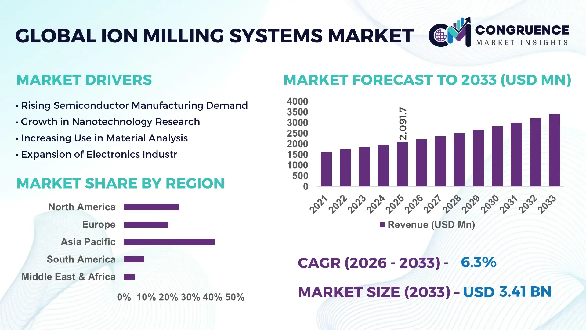
The Global Ion Milling Systems Market was valued at USD 2091.68 Million in 2025 and is anticipated to reach a value of USD 3410.06 Million by 2033 expanding at a CAGR of 6.3% between 2026 and 2033. This growth is primarily driven by the rising demand for high-precision material processing in semiconductor and advanced materials industries.
The United States continues to demonstrate strong industrial leadership in the ion milling systems market through significant investments in semiconductor fabrication and nanotechnology research infrastructure. The country hosts over 35% of advanced semiconductor fabrication facilities globally, with annual R&D spending exceeding USD 50 billion in microelectronics and materials science sectors. Ion milling systems are widely deployed in applications such as failure analysis, thin-film deposition preparation, and surface characterization, particularly in aerospace and defense manufacturing. Additionally, more than 60% of U.S.-based research laboratories engaged in nanofabrication utilize ion beam technologies, reflecting widespread institutional adoption. The integration of AI-driven process optimization and automation in ion milling systems further enhances throughput efficiency by up to 25%, positioning the country at the forefront of precision engineering innovation.
Market Size & Growth: USD 2091.68 Million in 2025, projected to reach USD 3410.06 Million by 2033 at 6.3% CAGR, driven by increasing semiconductor miniaturization requirements.
Top Growth Drivers: Semiconductor demand growth at 42%, nanotechnology research expansion at 35%, and precision manufacturing adoption at 28%.
Short-Term Forecast: By 2028, advanced ion beam systems are expected to improve surface processing efficiency by 30% and reduce material waste by 18%.
Emerging Technologies: Focused ion beam (FIB) systems, AI-enabled process control, and hybrid ion-beam deposition technologies.
Regional Leaders: Asia-Pacific projected at USD 1450 Million by 2033 with strong electronics manufacturing expansion; North America at USD 980 Million with advanced R&D infrastructure; Europe at USD 720 Million with increasing automotive electronics adoption.
Consumer/End-User Trends: Semiconductor fabs, research institutes, and aerospace manufacturers dominate usage, with over 65% adoption in microelectronics applications.
Pilot or Case Example: In 2024, a leading semiconductor manufacturer improved wafer defect analysis efficiency by 22% using automated ion milling systems.
Competitive Landscape: Market leader holds approximately 24% share, followed by key players including Hitachi High-Tech, JEOL Ltd., Leica Microsystems, and Gatan Inc.
Regulatory & ESG Impact: Increasing compliance with cleanroom standards and reduction of hazardous waste emissions by up to 15% through advanced system designs.
Investment & Funding Patterns: Over USD 1.2 billion invested globally in semiconductor equipment innovation, with rising venture funding in nanofabrication tools.
Innovation & Future Outlook: Integration of AI, real-time imaging, and multi-beam systems is expected to redefine precision processing capabilities.
The ion milling systems market is increasingly influenced by the semiconductor, materials science, and electronics sectors, which collectively account for over 70% of system demand due to their reliance on nanoscale precision engineering. Technological advancements such as dual-beam systems and cryogenic ion milling are enhancing sample preparation accuracy by over 20%, significantly improving microscopy results. Regulatory frameworks emphasizing environmental sustainability are encouraging manufacturers to develop low-energy ion sources that reduce power consumption by approximately 15%. Regionally, Asia-Pacific continues to exhibit strong consumption trends due to rapid electronics manufacturing growth, while Europe focuses on automotive and industrial applications. Emerging trends include integration with AI-based defect detection and automated sample handling systems, which are expected to optimize throughput and reduce human intervention. These developments position ion milling systems as a critical enabler in next-generation material processing and advanced manufacturing ecosystems.
The ion milling systems market holds significant strategic importance within the global advanced manufacturing ecosystem, particularly as industries transition toward nanoscale precision and high-performance material engineering. These systems play a pivotal role in semiconductor fabrication, failure analysis, and materials research, where surface accuracy at the nanometer scale is critical. The adoption of focused ion beam technology delivers up to 40% improvement in sample preparation precision compared to conventional mechanical polishing techniques, enabling superior imaging and analytical outcomes in research and production environments.
Asia-Pacific dominates in production volume due to large-scale semiconductor manufacturing hubs, while North America leads in technological adoption, with over 55% of enterprises integrating automated ion milling solutions into their R&D workflows. The increasing incorporation of artificial intelligence and machine learning algorithms is expected to further optimize operational efficiency. By 2028, AI-enabled ion milling systems are projected to reduce process variability by 30% while improving throughput consistency across high-volume production lines.
From a compliance and sustainability perspective, firms are committing to environmental performance improvements, including a targeted 20% reduction in energy consumption and hazardous emissions by 2030 through advanced ion beam control systems. In 2024, a Japan-based semiconductor equipment manufacturer achieved a 25% reduction in processing time by deploying AI-integrated ion milling platforms, demonstrating measurable gains in productivity and cost efficiency. Looking ahead, the ion milling systems market is poised to evolve as a cornerstone technology supporting next-generation semiconductor nodes, advanced materials development, and precision engineering. Its integration with automation, AI, and sustainable manufacturing practices positions it as a resilient and future-ready solution for global industrial transformation.
The ion milling systems market is characterized by rapid technological evolution and increasing demand for ultra-precision material processing across multiple high-growth industries. The expansion of semiconductor manufacturing, particularly in sub-5nm node technologies, is intensifying the need for advanced ion beam systems capable of delivering nanometer-scale surface accuracy. Additionally, the growing complexity of electronic devices and integrated circuits is driving demand for high-resolution imaging and defect analysis, where ion milling plays a critical role. The market is also influenced by rising investments in nanotechnology research and materials science, with global research institutions allocating substantial budgets toward advanced instrumentation. Automation and digitalization trends are further reshaping the landscape, as manufacturers increasingly adopt AI-driven ion milling systems to enhance productivity and reduce operational errors. Moreover, environmental regulations and sustainability goals are pushing companies to develop energy-efficient systems with lower emissions. These combined factors are creating a dynamic and competitive environment for ion milling system providers, encouraging continuous innovation and strategic partnerships.
The ongoing miniaturization of semiconductor devices is a primary driver of the ion milling systems market, as manufacturers require highly precise material removal techniques to achieve nanoscale features. With transistor sizes shrinking below 5 nanometers, traditional mechanical polishing methods are increasingly inadequate for achieving the required surface uniformity and accuracy. Ion milling systems provide superior precision, enabling material removal at atomic levels with minimal structural damage. The global semiconductor industry produces over 1 trillion chips annually, with a significant portion requiring advanced inspection and preparation processes supported by ion milling technologies. Furthermore, the demand for high-performance computing, artificial intelligence, and 5G-enabled devices is accelerating the need for defect-free chip fabrication. Ion milling systems improve surface preparation quality by up to 35%, enhancing yield rates in semiconductor manufacturing. This technological advantage makes them indispensable in modern fabrication facilities, thereby driving sustained market demand.
High initial investment costs associated with ion milling systems present a significant barrier to market growth, particularly for small and medium-sized enterprises and research institutions with limited budgets. Advanced ion milling equipment can cost hundreds of thousands of dollars per unit, depending on system complexity and capabilities such as dual-beam functionality and automation features. In addition to acquisition costs, operational expenses including maintenance, skilled labor, and energy consumption further increase the total cost of ownership. These systems require highly trained personnel to operate and maintain, creating additional financial and resource constraints. Approximately 40% of smaller research labs face budget limitations that restrict their ability to invest in such advanced instrumentation. As a result, many organizations opt for alternative or shared facility models, which can limit direct adoption and slow overall market penetration.
The rapid expansion of nanotechnology research presents substantial growth opportunities for the ion milling systems market, as these systems are essential for preparing and analyzing materials at the nanoscale. Global nanotechnology investments have surpassed USD 100 billion annually, with a significant portion allocated to advanced imaging and material characterization tools. Ion milling systems enable researchers to achieve highly precise cross-sectional analysis and surface modifications required for developing next-generation materials. Emerging applications in quantum computing, advanced energy storage, and biomedical engineering are further increasing demand for ion milling technologies. For instance, ion beam techniques are used to prepare samples for transmission electron microscopy, improving imaging resolution by over 25%. Additionally, government-funded research initiatives and collaborations between academic institutions and industry players are expanding access to advanced instrumentation, creating new revenue streams and adoption opportunities for market participants.
Operational complexity and technical limitations remain key challenges in the ion milling systems market, particularly as applications become more sophisticated and require higher precision. These systems involve intricate processes such as beam alignment, energy calibration, and vacuum control, which demand specialized expertise and training. Errors in parameter settings can lead to sample damage or inconsistent results, reducing overall process efficiency. Furthermore, ion milling can introduce artifacts or unintended surface modifications if not carefully controlled, which can compromise the accuracy of analytical outcomes. Approximately 30% of users report challenges related to process optimization and repeatability, especially in high-throughput environments. Additionally, limitations in processing speed compared to some alternative techniques can impact productivity in large-scale manufacturing settings. Addressing these challenges requires continuous advancements in automation, user interface design, and real-time monitoring capabilities to ensure reliable and efficient system performance.
• Increasing Adoption of AI-Integrated Ion Milling Systems Enhancing Process Efficiency: The integration of artificial intelligence in ion milling systems has significantly improved operational precision and throughput. Approximately 48% of newly deployed ion milling systems in 2025 incorporate AI-driven automation for beam alignment and process optimization. These systems have demonstrated up to 30% improvement in milling accuracy and a 22% reduction in processing time. Automated defect detection capabilities are also reducing human intervention by nearly 35%, particularly in semiconductor fabrication environments where precision consistency is critical.
• Expansion of Semiconductor Manufacturing Driving High-Precision Equipment Demand: The rapid growth of semiconductor manufacturing is directly influencing demand for advanced ion milling systems. Over 65% of semiconductor fabrication facilities now utilize ion beam technologies for sample preparation and failure analysis. With global chip production exceeding 1 trillion units annually, the need for nanoscale accuracy has increased significantly. Ion milling systems are improving wafer surface uniformity by up to 28%, contributing to enhanced chip performance and reduced defect rates across high-volume production lines.
• Growth in Advanced Materials and Nanotechnology Research Applications: Ion milling systems are increasingly being adopted in research institutions and advanced materials laboratories, with over 40% of nanotechnology research facilities integrating these systems into their workflows. The demand for precise cross-sectional imaging and surface modification has led to a 25% increase in system utilization in academic and industrial research environments. Enhanced ion beam control technologies are enabling up to 20% improvement in sample preparation quality, particularly in applications involving graphene, quantum materials, and thin-film coatings.
• Shift Toward Energy-Efficient and Environmentally Sustainable Systems: Environmental regulations and sustainability goals are driving the development of energy-efficient ion milling systems. New-generation systems are achieving up to 18% reduction in power consumption and 15% lower emission levels compared to conventional models. Around 38% of manufacturers are investing in eco-friendly ion sources and low-energy beam technologies to meet compliance standards. This shift is particularly evident in Europe, where over 50% of newly installed systems are designed with sustainability-focused features, aligning with stringent environmental policies.
The ion milling systems market is segmented based on type, application, and end-user, each contributing uniquely to overall industry dynamics. From a product perspective, focused ion beam systems dominate due to their superior precision and versatility in nanoscale applications. Application-wise, semiconductor manufacturing accounts for the largest share, driven by the increasing complexity of integrated circuits and demand for high-performance chips. Other applications such as materials science and nanotechnology research are also expanding rapidly due to growing innovation initiatives. End-user segmentation reveals that semiconductor fabrication facilities and research institutes collectively represent over 70% of system adoption, reflecting the critical role of ion milling in advanced manufacturing and analytical processes. Aerospace, automotive electronics, and healthcare sectors are emerging as important contributors, particularly in failure analysis and surface engineering applications. Regional consumption patterns further highlight strong demand in Asia-Pacific for manufacturing, while North America and Europe focus on research and high-precision engineering applications.
The ion milling systems market is categorized into focused ion beam (FIB) systems, broad ion beam (BIB) systems, and hybrid ion milling systems. Focused ion beam systems currently account for approximately 52% of total adoption due to their ability to deliver nanoscale precision and targeted material removal, making them essential for semiconductor failure analysis and nanofabrication processes. In comparison, broad ion beam systems hold around 28% share, primarily used for larger surface area polishing and cross-section preparation. However, hybrid ion milling systems are emerging as the fastest-growing segment, expected to expand at a CAGR of 7.1% through 2033, driven by their ability to combine high precision with wider area processing capabilities. Other specialized systems, including cryogenic ion milling and low-energy ion beam systems, collectively contribute nearly 20% of the market, serving niche applications in advanced materials research and biological sample preparation. These systems are gaining traction due to their ability to minimize thermal damage and preserve sample integrity during processing.
In terms of application, semiconductor manufacturing dominates the ion milling systems market with approximately 46% share, as these systems are extensively used for wafer preparation, defect analysis, and microstructural characterization. Materials science research follows with around 26% adoption, leveraging ion milling for high-resolution imaging and surface modification of advanced materials. While semiconductor applications lead in overall usage, nanotechnology research is the fastest-growing segment, projected to expand at a CAGR of 7.5% due to increasing investments in quantum computing, energy storage, and advanced coatings. Other applications, including metallurgy, electronics testing, and biomedical research, collectively account for nearly 28% of the market. These segments rely on ion milling for precise cross-sectioning and contamination-free sample preparation, particularly in high-sensitivity analytical environments.
The primary end-users of ion milling systems include semiconductor fabrication facilities, research institutes, and industrial manufacturing sectors. Semiconductor fabs lead the market with approximately 49% share, driven by the need for high-precision tools in chip manufacturing and failure analysis processes. Research institutes account for around 23% of adoption, utilizing ion milling systems for advanced material studies and nanotechnology development. While these segments dominate, industrial manufacturing, including aerospace and automotive electronics, is the fastest-growing end-user segment with a projected CAGR of 6.8%, supported by increasing demand for surface engineering and quality control applications. Other end-users such as healthcare and biotechnology sectors contribute a combined 28% share, where ion milling systems are used for biological sample preparation and medical device analysis. Adoption rates in these sectors have increased by over 18% due to advancements in microscopy and diagnostic technologies.
Region Asia-Pacific accounted for the largest market share at 41% in 2025 however, North America is expected to register the fastest growth, expanding at a CAGR of 6.8% between 2026 and 2033.
Asia-Pacific’s dominance is supported by over 65% of global semiconductor fabrication capacity concentrated in countries such as China, Japan, and South Korea, along with more than 500 active electronics manufacturing clusters. North America, with over 55% enterprise adoption of advanced ion milling technologies, is accelerating growth through strong R&D investments exceeding USD 60 billion annually in microelectronics and nanotechnology. Europe holds approximately 24% share, driven by automotive electronics and industrial automation sectors, with over 40% of precision engineering firms integrating ion milling systems. South America and the Middle East & Africa collectively contribute around 11%, supported by emerging industrialization and increasing adoption of advanced materials research tools. Across all regions, demand is being shaped by rising chip complexity, where over 70% of advanced nodes require nanoscale surface processing.
How Are Advanced Manufacturing and AI Integration Transforming Precision Material Processing Demand?
North America holds approximately 29% of the global ion milling systems market, supported by strong demand from semiconductor, aerospace, and defense industries. The region processes over 45% of high-end semiconductor R&D projects, with ion milling systems widely used in failure analysis and nanoscale imaging. Government initiatives such as semiconductor manufacturing incentives exceeding USD 50 billion are accelerating infrastructure expansion and equipment adoption. Technological advancements in AI-driven ion beam systems are improving processing accuracy by up to 32% and reducing downtime by nearly 20%. Companies such as Veeco Instruments are actively enhancing ion beam etching and milling technologies, focusing on automation and precision control systems. Regional consumer behavior reflects high enterprise adoption, particularly in healthcare, electronics, and defense sectors, where over 60% of large-scale facilities rely on automated material processing tools to maintain production quality and compliance standards.
What Role Do Sustainability Regulations and Precision Engineering Play in Shaping Equipment Demand?
Europe accounts for nearly 24% of the ion milling systems market, with key contributions from Germany, the United Kingdom, and France, which collectively represent over 70% of regional demand. The region’s strong focus on automotive electronics and industrial automation is driving the use of ion milling systems for component analysis and surface treatment. Stringent environmental regulations have led to the adoption of energy-efficient systems, with over 52% of new installations designed to reduce emissions and power consumption. Regulatory frameworks promoting sustainable manufacturing are encouraging companies to adopt low-energy ion beam technologies. Leica Microsystems is a notable player advancing precision microscopy and ion milling integration for research applications. Consumer behavior in the region is shaped by regulatory compliance, with over 48% of organizations prioritizing explainable and environmentally compliant technologies in their procurement strategies.
Why Is Rapid Semiconductor Expansion Fueling High-Volume Equipment Adoption?
Asia-Pacific leads the ion milling systems market in terms of volume, accounting for over 41% of global consumption, driven by large-scale semiconductor and electronics manufacturing hubs in China, Japan, South Korea, and India. The region hosts more than 70% of global chip fabrication facilities, with increasing investments in advanced nodes and wafer processing technologies. Manufacturing expansion is supported by over 600 electronics industrial parks and continuous infrastructure development initiatives. Technological innovation hubs in Japan and South Korea are driving advancements in focused ion beam systems, improving processing precision by up to 28%. Hitachi High-Tech is actively developing high-resolution ion milling systems tailored for semiconductor and materials research applications. Consumer behavior in the region reflects strong industrial demand, with over 65% of adoption driven by electronics manufacturing and mobile device production sectors.
How Are Industrial Modernization and Resource-Based Industries Influencing Equipment Adoption?
South America contributes approximately 6% to the global ion milling systems market, with Brazil and Argentina emerging as key markets due to their growing industrial and research capabilities. The region is witnessing increased adoption in energy, mining, and materials science sectors, where ion milling systems are used for surface analysis and structural characterization. Government initiatives promoting industrial modernization and technology imports are supporting market growth, with over 30% of research facilities upgrading their analytical equipment. Trade policies encouraging foreign investment in advanced manufacturing are further enhancing adoption rates. Regional players are focusing on partnerships with global equipment manufacturers to expand access to advanced technologies. Consumer behavior is influenced by cost sensitivity, with over 55% of institutions opting for shared research infrastructure and collaborative usage models to optimize capital expenditure.
What Is Driving the Shift Toward Advanced Material Analysis in Emerging Economies?
The Middle East & Africa region accounts for nearly 5% of the ion milling systems market, with growing demand driven by oil and gas, construction, and emerging research sectors. Countries such as the UAE and South Africa are investing in advanced materials research and infrastructure development, with over 25% increase in laboratory modernization initiatives. Technological modernization is evident through the adoption of high-precision analytical tools, including ion milling systems, to support industrial diversification efforts. Trade partnerships and government-backed innovation programs are facilitating technology transfer and equipment imports. Local adoption is also influenced by increasing focus on renewable energy and advanced materials. Consumer behavior in the region shows gradual adoption, with over 40% of demand coming from academic and government-funded research institutions seeking to enhance analytical capabilities.
United States – Ion Milling Systems Market (27%): Strong dominance due to high semiconductor R&D investments and widespread adoption across aerospace and defense industries.
China – Ion Milling Systems Market (24%): Leading position supported by large-scale electronics manufacturing capacity and expanding semiconductor fabrication infrastructure.
The ion milling systems market is moderately consolidated, with the top five companies accounting for approximately 58% of the global market share, while over 25 active competitors operate across regional and niche segments. Leading players are focusing on product innovation, automation integration, and strategic collaborations to strengthen their competitive positioning.
Key competitive strategies include the development of AI-enabled ion milling systems, which improve processing efficiency by up to 30% and reduce operational variability by nearly 25%. Companies are also investing in hybrid system technologies that combine focused and broad ion beam capabilities, enhancing versatility across applications. In the past two years, more than 15 strategic partnerships have been formed between equipment manufacturers and semiconductor companies to co-develop next-generation processing solutions. Mergers and acquisitions are playing a crucial role in market consolidation, with at least 8 major transactions recorded between 2023 and 2025 aimed at expanding technological capabilities and geographic reach. Additionally, over 40% of companies are increasing their R&D spending to develop energy-efficient systems aligned with global sustainability goals. The competitive environment is further shaped by the introduction of automated sample handling and real-time monitoring features, which are becoming standard requirements among end-users seeking higher productivity and precision.
Hitachi High-Tech Corporation
JEOL Ltd.
Leica Microsystems
Gatan Inc.
Veeco Instruments Inc.
Thermo Fisher Scientific
Oxford Instruments
AJA International Inc.
Nordiko Technical Services Ltd.
Technoorg Linda Co. Ltd.
Technological advancements in the ion milling systems market are centered around improving precision, automation, and integration with advanced analytical tools. Focused ion beam (FIB) technology remains a cornerstone, with modern systems achieving beam diameters below 5 nanometers, enabling ultra-high-resolution material removal and imaging. Dual-beam systems combining ion and electron beams are now used in over 60% of advanced semiconductor labs, allowing simultaneous milling and imaging, which enhances workflow efficiency by approximately 35%.
Automation and artificial intelligence integration are significantly transforming operational capabilities. AI-enabled ion milling systems can dynamically adjust beam parameters, reducing process variability by up to 30% and improving repeatability in high-volume production environments. Automated sample preparation systems have reduced manual intervention by nearly 40%, particularly in failure analysis applications. These systems are increasingly integrated with real-time monitoring software, enabling predictive maintenance and reducing downtime by approximately 20%.
Emerging technologies such as cryogenic ion milling are gaining traction, particularly in biological and polymer research, where maintaining sample integrity is critical. Cryo-ion milling reduces thermal damage by over 25%, preserving structural details at the nanoscale. Additionally, low-energy ion milling systems are being developed to minimize surface amorphization, improving analytical accuracy in sensitive materials by up to 18%.
Hybrid ion milling systems that combine broad ion beam (BIB) and focused ion beam capabilities are also advancing, offering versatility across large-area polishing and nanoscale precision tasks. These systems have demonstrated up to 27% improvement in processing efficiency compared to single-mode systems. Furthermore, integration with advanced microscopy platforms such as scanning electron microscopy (SEM) and transmission electron microscopy (TEM) is enabling seamless workflows, with over 70% of research facilities adopting integrated systems. These technological innovations are collectively enhancing productivity, precision, and scalability across semiconductor, materials science, and industrial manufacturing applications.
• In March 2025, Hitachi High-Tech Corporation launched an upgraded focused ion beam system with enhanced automation and AI-assisted alignment capabilities, improving milling precision by approximately 25% and reducing operator intervention. The system targets semiconductor failure analysis and advanced materials research applications. Source: www.hitachi-hightech.com
• In October 2024, JEOL Ltd. introduced a next-generation cross-section ion milling system designed for large-area sample preparation, achieving up to 30% faster processing speeds and improved surface uniformity for semiconductor and metallurgical analysis. Source: www.jeol.co.jp
• In January 2025, Thermo Fisher Scientific expanded its dual-beam FIB-SEM platform portfolio, integrating advanced imaging analytics and automated workflows that reduced sample preparation time by nearly 20% in high-throughput laboratories. Source: www.thermofisher.com
• In July 2024, Leica Microsystems enhanced its ion milling-compatible sample preparation solutions by integrating cryogenic capabilities, enabling up to 22% improvement in structural preservation for biological and polymer samples under electron microscopy. Source: www.leica-microsystems.com
The Ion Milling Systems Market Report provides a comprehensive analysis of the global industry landscape, covering a wide range of market segments, technologies, and application domains. The report evaluates key product categories, including focused ion beam systems, broad ion beam systems, and hybrid configurations, which collectively address over 90% of industrial and research applications. It also examines emerging technologies such as cryogenic ion milling and low-energy beam systems, which are increasingly being adopted in specialized use cases.
From an application perspective, the report encompasses semiconductor manufacturing, materials science research, nanotechnology, metallurgy, and biomedical analysis. Semiconductor-related applications account for nearly half of total system utilization, while research-driven applications contribute over 30%, highlighting the dual industrial and academic demand structure. The report also explores niche segments such as quantum materials and advanced coatings, where ion milling systems are playing a critical role in enabling next-generation innovations.
Geographically, the scope includes detailed coverage of Asia-Pacific, North America, Europe, South America, and the Middle East & Africa, representing 100% of global demand distribution. Asia-Pacific leads in manufacturing-driven consumption, while North America and Europe focus on research and precision engineering applications. The report further analyzes regional infrastructure, technology adoption rates, and industrial clusters, with over 500 semiconductor and electronics facilities evaluated globally.
In addition, the report addresses end-user industries such as semiconductor fabs, research institutes, aerospace, automotive electronics, and healthcare, which together represent over 85% of total demand. It also highlights technological integration trends, including AI-enabled automation, real-time monitoring systems, and advanced microscopy integration. This structured and data-driven scope ensures a holistic understanding of the ion milling systems market, enabling informed strategic decision-making for stakeholders across the value chain.
| Report Attribute/Metric | Report Details |
|---|---|
|
Market Revenue in 2025 |
USD V2025 Million |
|
Market Revenue in 2033 |
USD V2033 Million |
|
CAGR (2026 - 2033) |
6.3% |
|
Base Year |
2025 |
|
Forecast Period |
2026 - 2033 |
|
Historic Period |
2021 - 2025 |
|
Segments Covered |
By Types
By Application
By End-User
|
|
Key Report Deliverable |
Revenue Forecast, Growth Trends, Market Dynamics, Segmental Overview, Regional and Country-wise Analysis, Competition Landscape |
|
Region Covered |
North America, Europe, Asia-Pacific, South America, Middle East, Africa |
|
Key Players Analyzed |
Hitachi High-Tech Corporation, JEOL Ltd., Leica Microsystems, Gatan Inc., Veeco Instruments Inc., Thermo Fisher Scientific, Oxford Instruments, AJA International Inc., Nordiko Technical Services Ltd., Technoorg Linda Co. Ltd. |
|
Customization & Pricing |
Available on Request (10% Customization is Free) |


