
Reports
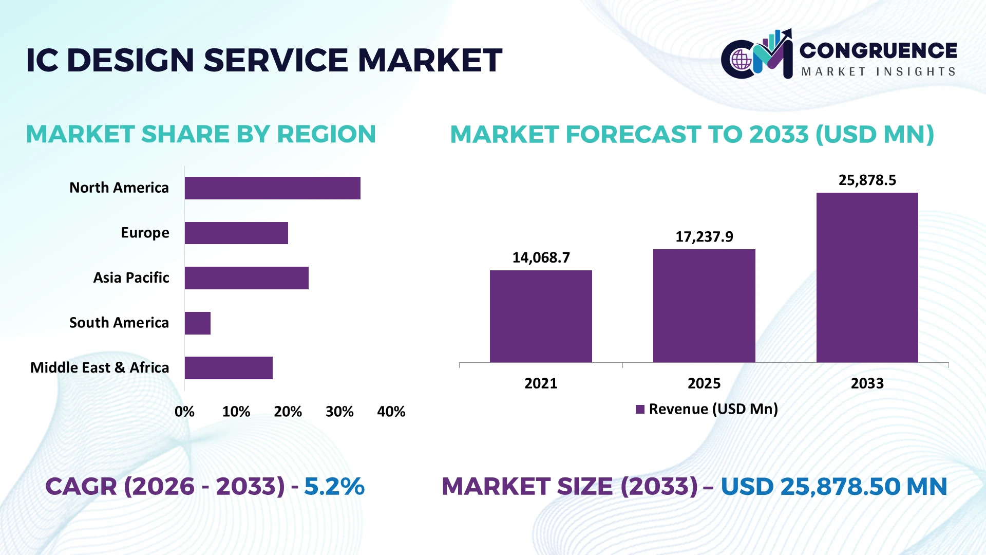
The Global IC Design Service Market was valued at USD 17237.85 Million in 2025 and is anticipated to reach a value of USD 25878.5 Million by 2033 expanding at a CAGR of 5.21% between 2026 and 2033. Growth is driven by increasing AI accelerator complexity, chiplet integration, advanced-node migration, and fabless semiconductor companies outsourcing verification, physical design, and IP development to accelerate tape-out schedules.
The United States remains the leading high-value IC design center, supported by AI, data-center, automotive, and communications semiconductor development, while India provides approximately 20% of the global semiconductor design workforce, creating substantial engineering capacity for outsourced design services. The U.S. CHIPS Act directs USD 52.7 billion toward semiconductor manufacturing, research, and workforce development, strengthening domestic ecosystem resilience amid U.S.-China technology restrictions.
Strategically, buyers should prioritize IC design partners with advanced-node, AI/HPC, chiplet, verification, and multi-region engineering capabilities.
Market Size & Growth: USD 17,237.85 million in 2025 is projected to reach USD 25,878.5 million by 2033 at a 5.21% CAGR, supported by AI, chiplets, and advanced semiconductor architectures.
Top Growth Drivers: AI/HPC chip development 32%, design outsourcing 24%, chiplet adoption 18%.
Short-Term Forecast: By 2028, AI-assisted design automation targets 10–15% higher engineering productivity and shorter verification cycles.
Emerging Technologies: AI-assisted EDA, chiplets, 2.5D/3D integration, and RISC-V are reshaping high-performance IC design workflows.
Regional Leaders: North America is projected at USD 9.1 billion, Asia-Pacific at USD 8.4 billion, and Europe at USD 4.2 billion, with AI, automotive, and communications adoption strengthening.
Consumer/End-User Trends: More than 60% of advanced electronics platforms increasingly incorporate dedicated AI or edge-computing capabilities, increasing demand for specialized IC design.
Pilot/Case Example: 2025 chiplet-oriented development programs demonstrated approximately 20% reductions in selected integration and verification cycles through reusable IP and modular architectures.
Competitive Landscape: Synopsys, Cadence, Arm, Broadcom, and NVIDIA remain prominent ecosystem participants, competing through advanced-node expertise, semiconductor IP, EDA integration, and AI-focused architectures.
Regulatory & ESG Impact: The USD 52.7 billion U.S. CHIPS Act is accelerating domestic semiconductor capacity and strengthening geographically diversified design-to-manufacturing strategies.
Investment & Funding: More than USD 50 billion in major semiconductor ecosystem commitments during the recent expansion cycle are supporting fabs, advanced packaging, R&D, and associated design capabilities.
Innovation & Future Outlook: AI-native EDA, 3D ICs, chiplets, advanced packaging, and domain-specific accelerators are shifting competition toward reusable IP, faster verification, and design productivity.
The IC Design Service Market is gaining strategic importance across AI accelerators, automotive electronics, data-center processors, networking silicon, and edge devices. Demand increasingly centers on advanced-node implementation, reusable semiconductor IP, AI-enabled verification, and chiplet integration, with AI-assisted EDA delivering roughly 10–15% productivity gains in targeted workflows. At the same time, geopolitical semiconductor localization is encouraging geographically diversified engineering capacity, creating a stronger strategic case for specialized IC design partners.
IC design services are becoming strategically important because semiconductor companies compete increasingly on architecture, time-to-tape-out, power efficiency, and specialized computing rather than fabrication alone. AI accelerators, automotive SoCs, networking processors, and edge devices are increasing design complexity, pushing fabless companies toward external expertise for verification, physical design, semiconductor IP, and advanced-node implementation. Outsourcing selected engineering workloads can reduce internal design-cycle requirements by around 15%.
Supply-chain restructuring is further changing investment priorities. The United States is strengthening domestic semiconductor capabilities, while India is expanding its role as a high-volume engineering hub with roughly 20% of the global semiconductor design workforce. By contrast, Taiwan remains concentrated in advanced semiconductor manufacturing and ecosystem integration, creating complementary rather than identical competitive advantages.
Over the next 2–3 years, AI-assisted EDA adoption is positioned to improve targeted engineering productivity by 10–15%, while chiplet-based architectures increasingly support modular system development. A practical deployment example is automotive semiconductor development, where reusable IP and automated verification allow design teams to shorten validation cycles. Companies are therefore increasing partnerships with specialized design firms and prioritizing AI, chiplets, 3D integration, and advanced-node expertise. Competitive advantage will increasingly depend on combining engineering scale with faster, reusable design execution.
AI and high-performance computing architectures are intensifying demand for specialized IC design capabilities, with AI-assisted EDA workflows delivering approximately 10–15% productivity gains and automated verification reducing selected engineering cycles by nearly 20%. U.S. data-center accelerator development and automotive semiconductor programs are accelerating this shift from conventional design outsourcing toward architecture-level collaboration. Companies are responding by expanding AI-chip engineering teams, acquiring specialized IP capabilities, and forming partnerships covering verification, physical design, and packaging. The non-obvious advantage is faster reuse: modular IP can allow engineering teams to adapt proven blocks across multiple products instead of rebuilding designs for every tape-out, improving resource utilization and shortening commercialization schedules.
Advanced-node IC design remains constrained by escalating EDA licensing, verification, IP, and engineering costs, with specialized development programs frequently requiring 15–25% higher engineering budgets than mature-node projects. Dependence on concentrated semiconductor ecosystems also exposes companies to geopolitical restrictions affecting technology access, particularly across U.S.-China supply chains. These pressures increase project-cost volatility and complicate predictable capacity planning. Companies are responding through multi-year EDA contracts, reusable IP libraries, geographically diversified engineering teams, and selective migration to mature nodes where performance requirements permit. A key operational insight is that the lowest-cost design partner is not necessarily the most competitive; verification quality and first-pass silicon success increasingly determine total program economics.
Chiplet architectures create an important opportunity for IC design service providers because modular silicon enables companies to combine specialized functions without developing an entire monolithic die. Adoption of advanced packaging and chiplet methodologies is expected to expand engineering demand, while AI-assisted workflows can deliver roughly 10–15% productivity improvements in targeted design activities. India is particularly positioned to capture outsourced chiplet verification and physical-design workloads through its large semiconductor engineering base. Companies are increasing R&D around reusable IP, 2.5D/3D integration, and die-to-die interfaces while partnering across the semiconductor ecosystem. The strategic opportunity lies in becoming an integration partner rather than a task-based vendor, capturing higher-value architecture, verification, and system-level design work.
IC design execution faces a widening skills gap across advanced-node physical design, functional verification, chiplet integration, and AI accelerator architecture. Specialized engineering shortages can increase project timelines by 10–15%, while complex multi-die systems introduce additional verification and interoperability requirements. India is expanding semiconductor education and engineering capacity, but advanced expertise remains concentrated among established semiconductor hubs. Cybersecurity also becomes more critical as distributed design teams exchange proprietary RTL, IP, and verification assets across borders. Companies must therefore invest in secure collaborative design environments, continuous workforce training, automated verification, and standardized IP management. Long-term competitiveness will depend less on engineering headcount alone and more on integrating specialized talent, automation, cybersecurity, and reusable design infrastructure into one scalable workflow.
AI-Assisted Design Workflows: Generative AI and machine-learning-enabled EDA are moving from pilot use into verification, optimization, and physical-design workflows, with targeted productivity gains of 10–15% and selected tasks compressed from days to hours. Companies are expanding AI-enabled engineering teams to address advanced-node complexity and talent shortages.
Cloud-Based Engineering Expansion: Cloud EDA adoption is increasing as distributed teams require scalable compute, with infrastructure utilization improving roughly 15% and provisioning cycles falling 20%. U.S. and Indian design centers are shifting selected workloads to shared environments, reducing idle capacity while supporting cross-border collaboration and faster project scaling.
Chiplet Verification Intensifies: Chiplet-based architectures are increasing demand for interoperability testing, reusable IP, and multi-die verification, with integration workloads rising approximately 20% and reusable design blocks reducing selected development effort by 15%. Companies are restructuring partnerships around packaging, IP, and system-level verification rather than standalone design tasks.
Geopolitical Design Localization: U.S.-China technology restrictions and semiconductor localization programs are accelerating multi-country engineering footprints, with companies targeting 10–15% greater geographic diversification of critical design activities. India is gaining outsourced workloads while U.S. firms strengthen domestic capabilities, creating a non-obvious shift toward dual-location engineering models that improve continuity rather than simply lowering labor costs.
Digital IC Design remains the leading type, accounting for an estimated 48% share, supported by processor, memory, networking, AI accelerator, and embedded-system requirements. Its scalability and compatibility with automation give it a clear cost and productivity advantage, while advanced verification tools are improving design throughput by roughly 12%. Analog IC Design remains strategically important for power management and sensor interfaces, while Mixed-Signal IC Design benefits from increasing system integration and typically commands more specialized engineering resources.
Mixed-Signal IC Design is the fastest-growing type, expanding its adoption base as automotive, industrial, and connected-device platforms combine digital processing with analog sensing and power functions. Demand for integrated signal chains is increasing design complexity by approximately 15%, encouraging companies to strengthen mixed-signal verification capabilities and specialist partnerships. RF IC Design remains concentrated in wireless connectivity and telecommunications, where performance optimization and frequency-specific expertise remain decisive.
Consumer Electronics represents the leading application, with an estimated 36% share, supported by smartphones, wearables, smart-home devices, and computing products requiring compact, power-efficient silicon. High-volume product cycles favor reusable IP and automated verification, while AI-enabled functionality is increasing semiconductor design complexity by approximately 15%. Telecommunications remains a mature application, but higher networking throughput continues supporting specialized RF and digital IC requirements.
Automotive Electronics is the fastest-growing application, driven by electrification, ADAS, digital cockpits, and zonal architectures. Automotive design workloads are increasing roughly 12–18% as semiconductor content rises per vehicle, encouraging OEMs and suppliers to establish closer design partnerships and longer development programs. Industrial Electronics and IoT Devices remain important for automation, sensing, and connected equipment, with IoT-driven semiconductor requirements increasingly emphasizing low-power processing and secure connectivity.
Semiconductor Companies represent the dominant end-user group, with an estimated 42% share, because fabless firms and integrated manufacturers continuously require architecture, RTL development, verification, physical design, and IP integration. Their outsourcing intensity is increasing approximately 15% as advanced-node programs demand specialized expertise. Electronics OEMs and Consumer Electronics Manufacturers remain important buyers, particularly where proprietary silicon improves product differentiation and power efficiency.
Automotive OEMs are the fastest-growing end-user group as software-defined vehicles, ADAS, EV power electronics, and centralized computing increase direct involvement in semiconductor roadmaps. Their IC design-service requirements are expanding approximately 12%, with longer-term partnerships replacing isolated project procurement. Telecom Equipment Manufacturers continue prioritizing networking and RF performance, while OEM buyers increasingly seek customized engagement models, co-development, and dedicated engineering teams rather than generic outsourcing capacity.
North America accounted for the largest market share at 42% in 2025 however, Asia-Pacific is expected to register the fastest growth, expanding at a CAGR of 6.8% between 2026 and 2033.
AI-Centric Semiconductor Development Is Reshaping Design Capacity
North America commands approximately 42% of the global IC design service market, supported by dense activity across AI accelerators, data-center processors, automotive semiconductors, networking silicon, aerospace electronics, and high-performance computing. The United States represents the region's primary design center, where fabless semiconductor companies increasingly outsource RTL development, verification, physical design, and semiconductor IP integration to accelerate tape-out schedules. AI and advanced-node programs are increasing demand for specialized engineering capabilities by roughly 15%, while cloud-based EDA environments are improving distributed design utilization. U.S. semiconductor localization initiatives are also strengthening coordination between design, fabrication, advanced packaging, and testing. Companies are responding through engineering-center expansion, specialist acquisitions, and long-term design partnerships. The principal competitive advantage is shifting from low-cost engineering capacity toward architecture expertise, advanced verification capability, and faster design-to-silicon execution.
United States Market Outlook: The United States remains the most influential IC design hub because of its concentration of fabless semiconductor companies, EDA expertise, AI-chip developers, and high-performance computing programs. AI accelerator and data-center silicon development continues to increase demand for specialized front-end and back-end engineering. Domestic semiconductor investment and supply-chain localization are additionally encouraging companies to maintain critical design capabilities closer to strategic manufacturing and packaging infrastructure.
Automotive and Industrial Silicon Are Reshaping Design Priorities
Europe accounts for approximately 21% of global IC design service activity, with Germany, the Netherlands, France, and the United Kingdom providing strong capabilities across automotive electronics, industrial systems, telecommunications, power management, and embedded computing. Automotive semiconductor development is particularly influential as electrification, ADAS, centralized computing, and software-defined vehicle architectures increase semiconductor content per vehicle. European semiconductor programs are also emphasizing supply-chain resilience, functional safety, energy efficiency, and advanced packaging. Automotive and industrial applications are generating roughly 12% higher demand for specialized mixed-signal, embedded, and safety-oriented design capabilities. Companies are responding through cross-border R&D partnerships, semiconductor ecosystem alliances, and greater investment in reusable IP and verification automation. Europe's strategic strength is its ability to combine semiconductor design with deep automotive and industrial domain knowledge, allowing providers to compete on reliability, customization, and certification expertise rather than engineering cost alone.
Germany Market Outlook: Germany represents Europe's strongest IC design opportunity because automotive OEMs, Tier-1 suppliers, industrial manufacturers, and semiconductor companies are concentrated around sophisticated electronics development programs. Demand is expanding for ADAS processors, power-management ICs, automotive networking, and safety-critical embedded silicon. Functional-safety requirements are increasing verification intensity, strengthening the position of design providers with specialized validation and certification capabilities.
Manufacturing Scale Is Driving Tighter Design-to-Silicon Integration
Asia-Pacific represents approximately 34% of global IC design service activity and holds the strongest ecosystem concentration across semiconductor design, fabrication, packaging, testing, and electronics manufacturing. Taiwan anchors advanced-node manufacturing and foundry-linked design services, South Korea combines memory and consumer-electronics expertise, China maintains a broad electronics supply chain, and India provides a rapidly expanding engineering base. India accounts for approximately 20% of the global semiconductor design workforce, supporting outsourced verification, physical design, embedded systems, and IP development. Supply-chain restructuring is encouraging companies to establish multi-country engineering footprints connecting India with Taiwan and other manufacturing hubs. Companies are also expanding partnerships across chip design, advanced packaging, and foundry services to reduce iteration delays. The region's non-obvious advantage is ecosystem proximity: design teams can coordinate more efficiently with fabrication, packaging, and testing partners, improving design validation and accelerating production readiness.
Taiwan Market Outlook: Taiwan remains strategically central to advanced IC design because of its tightly integrated foundry, semiconductor IP, packaging, testing, and equipment ecosystem. Its concentration of advanced manufacturing capability supports rapid design iteration for AI accelerators, networking processors, mobile silicon, and high-performance computing. Close designer-foundry coordination also enables complex designs to move efficiently from physical implementation into silicon validation and volume manufacturing.
Application-Specific Silicon Is Expanding Beyond Traditional Electronics
South America remains a developing IC design service market, with Brazil representing the strongest concentration of semiconductor engineering, electronics manufacturing, telecommunications infrastructure, and technology development. Demand is centered on automotive electronics, industrial automation, payment systems, telecommunications equipment, embedded systems, and connected devices rather than advanced-node mass production. Local semiconductor initiatives are encouraging greater development of application-specific ICs, while limited domestic advanced-node fabrication capacity keeps many programs dependent on overseas foundries. Companies are therefore emphasizing design specialization, international fabrication partnerships, and localized engineering rather than capital-intensive manufacturing. Selected collaborative design programs can reduce engineering expenditure by approximately 10% through shared IP and external verification resources. Brazil's strategic value lies in customer proximity and application customization, enabling design providers to address local requirements while accessing international manufacturing infrastructure. This creates a partnership-led model rather than a vertically integrated semiconductor ecosystem.
Brazil Market Outlook: Brazil provides the most developed platform for IC design services in South America through its electronics manufacturing base, engineering workforce, telecommunications infrastructure, and demand from automotive and industrial customers. Local semiconductor initiatives are supporting specialized chip development while international foundry relationships provide access to advanced fabrication. Providers focused on embedded, mixed-signal, power-management, and application-specific designs are positioned to capture localized demand without requiring domestic leading-edge fabs.
AI Infrastructure Investment Is Creating New Silicon Requirements
Middle East & Africa remains an emerging IC design service market, increasingly influenced by data-center construction, telecommunications modernization, smart-city infrastructure, industrial digitization, and government-backed technology programs. The United Arab Emirates and Saudi Arabia are developing AI and cloud infrastructure while building broader technology ecosystems, creating demand for networking processors, power-management ICs, accelerators, and embedded solutions. South Africa contributes established electronics and engineering capabilities, particularly for industrial and telecommunications applications. AI, cloud, and digital-infrastructure projects now account for an estimated 10% of regional semiconductor engineering activity, increasing demand for specialized design expertise. Companies are responding through international technology partnerships, local engineering centers, and ecosystem-development agreements rather than large-scale fabrication investments. The region's most important competitive opportunity is application-focused IC design supporting digital infrastructure, where proximity to large technology projects can compensate for limited local semiconductor manufacturing depth.
United Arab Emirates Market Outlook: The United Arab Emirates is emerging as a strategically important IC design location because of its investment in AI infrastructure, cloud computing, data centers, and advanced digital services. International technology partnerships are expanding access to semiconductor expertise, while strong connectivity and enterprise infrastructure support specialized processor and networking applications. Companies establishing engineering capabilities in the UAE can serve regional AI and digital-infrastructure programs while connecting to global semiconductor ecosystems.
The IC Design Service Market is led by technology-intensive providers including Synopsys, Cadence Design Systems, Arm, Broadcom, and Alchip, competing with regional engineering specialists and semiconductor design houses. The top five players collectively account for approximately 28% of market activity, indicating a moderately concentrated structure driven by advanced technical capabilities rather than scale alone. Competition increasingly centers on advanced-node execution, AI-enabled EDA, verification quality, customization, and delivery speed. AI-assisted workflows can improve targeted engineering productivity by 10–15%, while reusable IP reduces selected development effort by nearly 20%. Global leaders are expanding through acquisitions, ecosystem partnerships, cloud-based design platforms, and AI-enabled automation. Regional providers compete through specialized talent, cost efficiency, and proximity to Indian and Asian semiconductor programs. Geopolitical supply-chain restructuring is further shifting competition toward geographically diversified delivery models. High EDA costs, proprietary IP, advanced verification requirements, cybersecurity, and specialized talent remain major entry barriers. Winning providers must combine technical depth, secure multi-country delivery, reusable IP, rapid execution, and long-term customer partnerships.
Synopsys, Inc.
Cadence Design Systems, Inc.
Arm Holdings plc
Broadcom Inc.
NVIDIA Corporation
MediaTek Inc.
Marvell Technology, Inc.
Alchip Technologies, Ltd.
GUC (Global Unichip Corp.)
Faraday Technology Corporation
Wipro Limited
HCLTech
Tata Elxsi
eInfochips
AI-assisted electronic design automation is moving into synthesis, verification, placement, routing, and optimization, with workflows delivering 10–15% productivity improvements and selected tasks moving from days to hours. Adoption is strongest among advanced-node and AI-chip teams, where automated optimization improves engineering throughput and reduces manual iteration. Cloud EDA is also expanding distributed compute access, giving design teams capacity scaling without duplicating infrastructure.
Chiplet architectures, 2.5D/3D integration, and advanced packaging are emerging as core design technologies, with reusable IP and modular verification reducing development effort by 15–20%. Compared with legacy monolithic implementation, chiplet-based reuse can improve iteration efficiency by roughly 20% while supporting heterogeneous integration. Adoption is accelerating across AI, HPC, networking, and automotive programs. Companies combining chiplet expertise with certified foundry flows gain competitive advantage through faster customization and lower integration risk.
Through 2026–2028, agentic EDA, AI-driven physical design, digital twins, and silicon-proven IP will integrate into workflows. AI-assisted engineering can compress optimization cycles by 20–30%, while automated verification strengthens first-pass execution. Competitive beneficiaries will be providers with advanced-node credentials, reusable IP libraries, secure cloud infrastructure, and foundry partnerships. Acting now enables design-service firms to capture architecture and system-level engagements as semiconductor complexity rises.
April 2026 Cadence expanded its TSMC collaboration with agent-ready digital and analog flows across N3, N2, A16 and A14 nodes. The partnership integrates AI-driven design, 3D-IC and signoff platforms, reducing iterations and strengthening competitive positioning for advanced AI silicon. Source: Cadence cadence.com
December 2025 NVIDIA invested $2 billion in Synopsys under an expanded multi-year collaboration. The companies integrated computing and AI across chip design and verification, with Synopsys projecting circuit-simulation gains up to 30x on NVIDIA Grace Blackwell, improving design throughput. Source: Reuters reuters.com
January 2025 SEMI reported 18 fabs expected to begin construction globally, including 15 300mm facilities. Advanced-node capacity at 7nm and below was projected to rise 16%, increasing demand for physical design, verification, IP integration, and engineering services. Source: SEMI semi.org
May 2025 Renesas opened two 3nm chip design centers in Noida and Bengaluru. The facilities expanded India's advanced-node engineering footprint and strengthened semiconductor capabilities, giving IC design teams greater access to infrastructure and supporting collaboration with global technology ecosystems. Source: India Today indiatoday.in
The IC Design Service Market Report covers Analog IC Design, Digital IC Design, Mixed-Signal IC Design, and RF IC Design across Consumer Electronics, Automotive Electronics, Telecommunications, Industrial Electronics, and IoT Devices. End-user coverage includes Semiconductor Companies, Electronics OEMs, Automotive OEMs, Telecom Equipment Manufacturers, and Consumer Electronics Manufacturers. The analysis evaluates design outsourcing, semiconductor IP integration, verification, physical design, advanced-node implementation, chiplet architectures, AI-assisted EDA, and 2.5D/3D IC technologies.
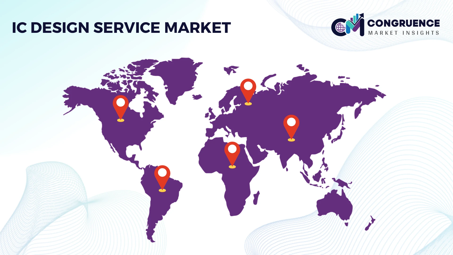
Geographic coverage spans North America, Europe, Asia-Pacific, South America, and the Middle East & Africa, with country-level assessment of engineering capacity, semiconductor ecosystems, manufacturing linkages, and investment activity. The report examines adoption patterns, competitive positioning, technology deployment, and shifting supply-chain strategies through 2026–2033. These insights support investment planning, market-entry decisions, engineering-capacity expansion, partnership selection, technology prioritization, and competitive strategy across high-value IC design workflows.
| Report Attribute/Metric | Report Details |
|---|---|
Market Revenue in 2025 | USD 17237.85 Million |
Market Revenue in 2033 | USD 25878.5 Million |
CAGR (2026 - 2033) | 5.21% |
Base Year | 2025 |
Forecast Period | 2026 - 2033 |
Historic Period | 2021 - 2025 |
Segments Covered | By Type
By Application
By End-User
|
Key Report Deliverable | Revenue Forecast, Growth Trends, Market Dynamics, Segmental Overview, Regional and Country-wise Analysis, Competition Landscape |
Region Covered | North America, Europe, Asia-Pacific, South America, Middle East, Africa |
Key Players Analyzed | Synopsys, Inc., Cadence Design Systems, Inc., Arm Holdings plc, Broadcom Inc., NVIDIA Corporation, MediaTek Inc., Marvell Technology, Inc., Alchip Technologies, Ltd., GUC (Global Unichip Corp.), Faraday Technology Corporation, Wipro Limited, HCLTech, Tata Elxsi, eInfochips |
Customization & Pricing | Available on Request (10% Customization is Free) |