
Reports
The Global Hybrid Bonding Equipment Market was valued at USD 364.75 Million in 2025 and is anticipated to reach a value of USD 631.42 Million by 2033 expanding at a CAGR of 7.1% between 2026 and 2033. Scaling advanced semiconductor packaging for AI accelerators, high-bandwidth memory, and chiplet architectures is accelerating investments in high-precision hybrid bonding equipment with tighter alignment accuracy and higher wafer throughput.
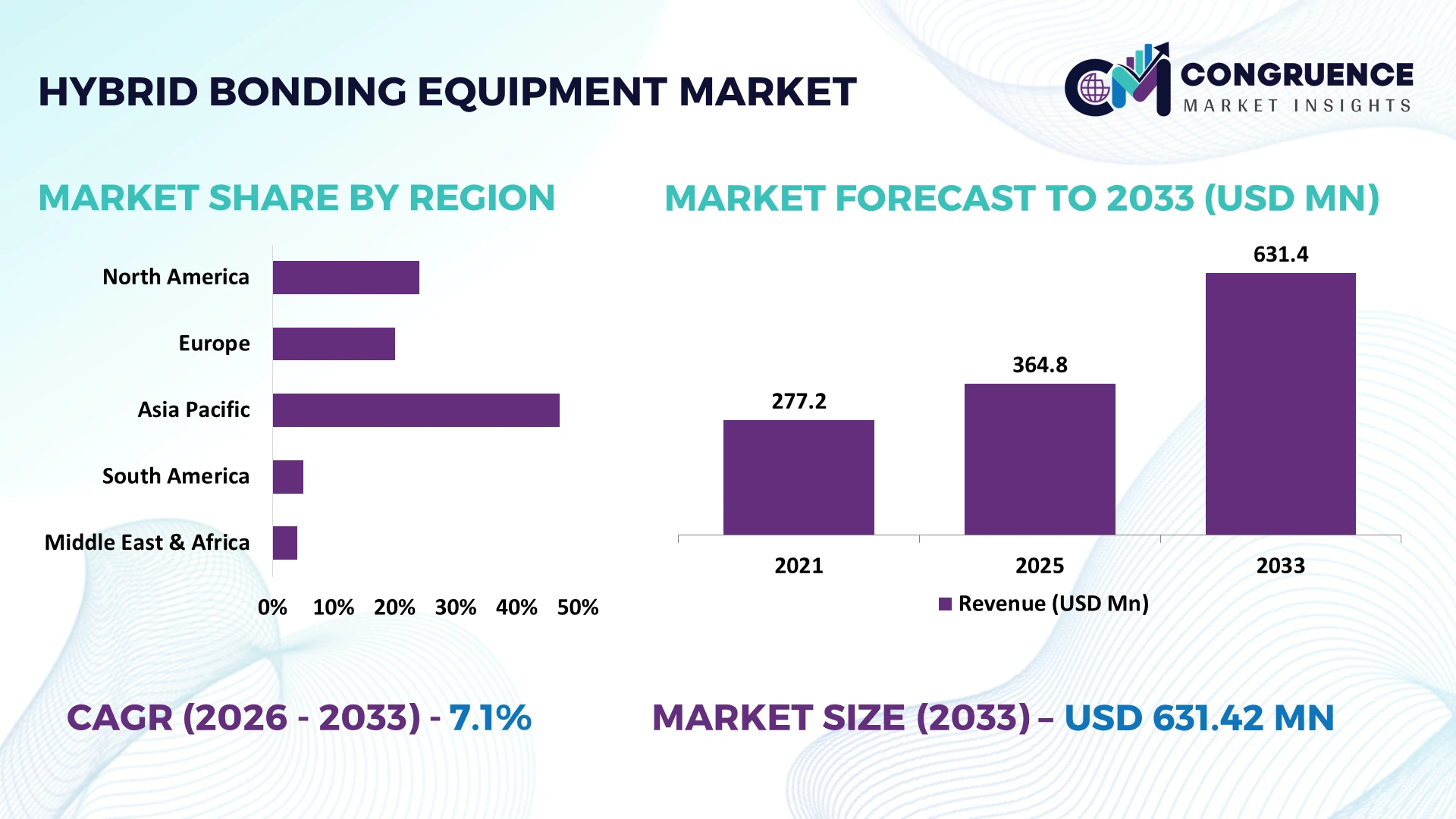
Taiwan dominates the global Hybrid Bonding Equipment Market with approximately 41% advanced packaging capacity, supported by sustained investments in semiconductor manufacturing and widespread adoption of wafer-level integration technologies across leading foundries. South Korea follows with nearly 24% capacity, driven by memory chip production and advanced packaging expansion, while 2026 supply-chain diversification across Asia strengthens equipment localization and production resilience. This leadership positions Asia-Pacific as the primary destination for capacity expansion, technology partnerships, and long-term equipment procurement strategies.
Market Size & Growth: USD 364.75 Million in 2025, projected to reach USD 631.42 Million by 2033 at 7.1% CAGR, supported by rapid adoption of chiplet integration and advanced semiconductor packaging.
Top Growth Drivers: AI semiconductor demand (+28%), advanced packaging investments (+21%), and high-bandwidth memory deployment (+18%) continue accelerating equipment purchases.
Short-Term Forecast: By 2028, bonding alignment precision improves by 20% while production cycle time declines by approximately 15% through automation upgrades.
Emerging Technologies: AI-driven process control, fully automated wafer handling, and sub-micron alignment systems improve production consistency by nearly 25%.
Regional Leaders: Asia-Pacific exceeds USD 330 Million by 2033 with rapid fab expansion; North America approaches USD 145 Million through domestic semiconductor programs; Europe surpasses USD 90 Million with advanced packaging localization.
Consumer/End-User Trends: More than 65% of leading semiconductor manufacturers prioritize hybrid bonding for next-generation logic-memory integration and heterogeneous packaging.
Pilot/Case Example: In 2026, advanced production-line implementation improved wafer yield by approximately 14% while reducing bonding defects by 17%.
Competitive Landscape: Leading suppliers collectively account for roughly 58% market share, with EV Group, Applied Materials, Tokyo Electron, ASMPT, and Besi driving technology leadership.
Regulatory & ESG Impact: Energy-efficient manufacturing initiatives reduce equipment power consumption by nearly 12%, supported by semiconductor localization policies and sustainability targets.
Investment & Funding: More than USD 3 Billion in semiconductor packaging investments support equipment expansion through strategic partnerships, regional manufacturing, and capacity upgrades amid global supply-chain realignment.
Innovation & Future Outlook: Next-generation hybrid bonding platforms integrate AI inspection and digital process optimization, enabling over 30% faster qualification cycles and strengthening high-performance computing manufacturing strategies.
Hybrid Bonding Equipment Market demand is strengthening across AI processors, high-bandwidth memory, advanced logic devices, and heterogeneous semiconductor packaging, where sub-micron interconnect performance is becoming essential. Automation-enabled bonding platforms and precision inspection technologies improve production efficiency by nearly 22%, while semiconductor supply-chain localization and advanced packaging investments in 2026 accelerate equipment deployment, setting the stage for broader strategic capacity expansion and competitive differentiation.
Hybrid bonding equipment has become strategically important as semiconductor manufacturers transition toward chiplet-based architectures, AI processors, and advanced memory integration that require higher interconnect density and lower power consumption. Supply-chain restructuring in 2026 is encouraging packaging capacity expansion outside traditional manufacturing hubs, while national semiconductor initiatives are accelerating investment in advanced backend technologies. This shift is strengthening competition among equipment suppliers capable of delivering higher precision, automation, and production scalability.
Modern hybrid bonding platforms achieve alignment accuracy below 200 nanometers, improving bonding yield by approximately 18% while reducing process steps by nearly 15% compared with conventional thermo-compression bonding systems. Taiwan continues to lead commercial deployment through large-scale advanced packaging ecosystems, whereas the United States is expanding pilot production and domestic packaging infrastructure to improve supply resilience. Over the next two to three years, automated wafer-level bonding adoption is expected to exceed 55% across newly commissioned advanced packaging facilities, improving production consistency and equipment utilization.
A practical example includes semiconductor manufacturers integrating automated metrology and AI-enabled inspection directly into hybrid bonding production lines, reducing defect detection time by roughly 20%. Equipment vendors are responding through technology partnerships, localized service networks, and expanded application centers to accelerate customer qualification. Companies that combine precision engineering, automation, and ecosystem collaboration will secure stronger competitive positioning as advanced semiconductor packaging becomes a strategic manufacturing capability.
The rapid commercialization of AI processors, high-bandwidth memory, and chiplet integration is driving structural demand for advanced hybrid bonding platforms. More than 60% of next-generation high-performance computing packages now incorporate advanced packaging technologies, while wafer-level integration improves interconnect density by approximately 25% and lowers power consumption by nearly 15%. Japan and Taiwan continue expanding advanced packaging infrastructure to support growing semiconductor output, reinforcing equipment demand across production lines. Equipment manufacturers are increasing investment in precision alignment systems, automation software, and collaborative development programs with foundries, enabling faster process qualification and stronger manufacturing competitiveness while reducing production bottlenecks across advanced semiconductor ecosystems.
Hybrid bonding equipment deployment remains constrained by high capital expenditure, demanding process qualification, and dependence on specialized optical, vacuum, and precision motion components. Equipment lead times have increased by approximately 20% for selected high-precision modules, while advanced manufacturing facilities allocate nearly 30% higher installation budgets compared with conventional bonding systems. Export controls affecting semiconductor manufacturing technologies have further complicated procurement strategies for several countries. Companies are reducing operational exposure by localizing component sourcing, establishing multi-supplier agreements, and standardizing equipment platforms to improve procurement flexibility, shorten installation cycles, and stabilize long-term production planning despite ongoing supply-chain uncertainty.
The expansion of chiplet-based semiconductor architectures is creating opportunities beyond traditional logic manufacturing, particularly across automotive electronics, advanced networking, and edge AI applications. Automated hybrid bonding processes improve production throughput by approximately 22% while reducing packaging defects by nearly 16%, supporting wider industrial adoption. India and Singapore are strengthening semiconductor manufacturing ecosystems through packaging infrastructure initiatives and technology partnerships, creating new equipment demand. Leading suppliers are expanding application laboratories, investing in digital process optimization, and collaborating with research institutes to accelerate next-generation packaging solutions. Early participation in these ecosystems enables companies to secure long-term customer relationships and specialized manufacturing capabilities before broader market standardization.
Maintaining consistent sub-micron alignment accuracy across high-volume manufacturing remains a significant execution challenge as package complexity continues increasing. Production qualification cycles typically extend 25% longer for advanced hybrid bonding processes than for mature packaging technologies, while skilled process engineering shortages exceed 18% across several semiconductor manufacturing hubs. Integrating inspection systems, metrology platforms, and factory automation into unified production environments also increases operational complexity. Equipment suppliers must strengthen workforce development, software interoperability, predictive maintenance capabilities, and collaborative engineering partnerships to ensure reliable large-scale deployment, consistent manufacturing quality, and sustainable competitiveness as semiconductor packaging technologies become increasingly sophisticated.
Advanced Chiplet Integration Scaling Hybrid bonding deployment is accelerating as chiplet-based processor production expands, with advanced packaging utilization increasing by approximately 27% and wafer-level interconnect density improving by nearly 24%. Semiconductor manufacturers in Taiwan and the United States are redesigning production workflows to integrate hybrid bonding earlier in fabrication, reducing assembly complexity and shortening qualification cycles by around 15%. Equipment suppliers are expanding collaborative development programs and co-engineering partnerships to optimize process compatibility as advanced computing architectures become mainstream.
Factory Automation Reshapes Production AI-enabled process control, automated optical inspection, and predictive maintenance are reducing bonding defects by roughly 18% while increasing equipment utilization by nearly 16%. Labor availability challenges and tighter manufacturing quality requirements in Japan and South Korea are accelerating smart factory deployments across semiconductor packaging facilities. Companies are integrating digital manufacturing platforms with hybrid bonding equipment, enabling real-time process optimization, faster recipe adjustments, and improved operational consistency across multiple production sites.
Localized Supply Networks Expand Supply-chain diversification has reduced dependency on single-country sourcing, with localized component procurement increasing by approximately 21% during 2026. Semiconductor manufacturers are establishing regional supplier ecosystems to improve equipment availability and reduce logistics exposure following continued export-control adjustments. Equipment vendors are responding by expanding regional service centers, strengthening local component partnerships, and restructuring procurement strategies to improve installation timelines and customer support responsiveness.
Precision Metrology Gains Priority Integrated metrology and in-line inspection adoption has increased by nearly 30%, enabling process variation reductions approaching 17% across advanced packaging lines. Rather than focusing only on bonding speed, manufacturers increasingly prioritize measurement accuracy and process repeatability as package complexity grows. Equipment developers are investing in high-resolution inspection platforms, software analytics, and unified quality-control architectures, creating a competitive advantage through higher first-pass yields and reduced production rework.
Fully Automatic equipment dominates the Hybrid Bonding Equipment Market with an estimated 44% market share, supported by superior throughput, repeatable sub-micron alignment, and reduced operator intervention across high-volume semiconductor manufacturing. Automated platforms improve production efficiency by approximately 20% while lowering defect rates by nearly 15%, making them the preferred choice for advanced foundries. Wafer-to-Wafer bonding remains the established solution for memory and logic manufacturing where production uniformity is critical, while Die-to-Wafer continues expanding as heterogeneous integration becomes increasingly important for AI and high-performance computing devices.
Die-to-Wafer represents the fastest-growing segment as semiconductor manufacturers seek greater design flexibility and higher chip utilization, with deployment increasing by approximately 23% across advanced packaging projects. Die-to-Die bonding maintains strategic relevance for specialized, high-value applications requiring selective integration despite lower production volumes. Equipment suppliers are prioritizing automation software, modular system architectures, and collaborative engineering partnerships to strengthen product differentiation and support increasingly complex packaging requirements, shifting investment toward flexible production platforms capable of supporting multiple bonding configurations.
3D IC Packaging holds the leading position with approximately 39% of market demand, driven by increasing deployment of chiplet architectures, AI accelerators, and high-performance computing devices requiring ultra-high interconnect density. Manufacturers report around 22% higher packaging efficiency through advanced hybrid bonding integration while reducing electrical resistance across stacked devices. Memory Devices remain a major application because high-bandwidth memory increasingly depends on advanced bonding precision, whereas CMOS Image Sensors continue adopting hybrid bonding for improved pixel density and imaging performance.
Logic Devices represent the fastest-growing application as advanced processors require tighter integration between computing cores and specialized accelerators. Deployment across logic packaging has increased by approximately 25%, encouraging equipment vendors to expand automated process control and integrated inspection capabilities. Companies are strengthening collaborations with semiconductor manufacturers, scaling application-specific equipment platforms, and accelerating technology qualification programs to meet growing operational requirements across AI, automotive electronics, and next-generation computing systems.
The Semiconductor industry accounts for approximately 61% of total equipment demand because advanced fabrication facilities require consistent precision, high-volume throughput, and reliable wafer-level integration. Hybrid bonding deployment across semiconductor manufacturing has improved packaging productivity by nearly 20% while reducing interconnect limitations by approximately 18%. Electronics manufacturers continue adopting hybrid bonding for compact consumer devices, whereas Telecommunications companies increasingly require advanced packaging to support high-speed networking hardware and AI-enabled infrastructure.
Automotive represents the fastest-growing end-user segment as autonomous driving platforms, advanced driver-assistance systems, and high-performance vehicle processors demand more sophisticated semiconductor packaging. Automotive-related hybrid bonding adoption has increased by approximately 24%, encouraging equipment suppliers to customize production solutions, establish long-term technology partnerships, and expand application engineering support. Companies are strengthening ecosystem collaborations, developing sector-specific process recipes, and offering scalable automation platforms to capture emerging demand while maintaining strong relationships with established semiconductor customers.
Asia-Pacific accounted for the largest market share at 57.8% in 2025 however, North America is expected to register the fastest growth, expanding at a 7.8% between 2026 and 2033.
Advanced Packaging Reshoring Accelerates Capacity Expansion
North America is strengthening its position through semiconductor reshoring, advanced packaging investments, and increased deployment of hybrid bonding technologies for AI processors and defense-grade electronics. The region represents approximately 21% of global market activity, supported by expanding packaging infrastructure and strong collaboration between foundries, equipment suppliers, and research institutions. More than 35% of newly announced advanced semiconductor packaging projects now incorporate hybrid bonding capability as manufacturers prioritize lower latency and higher interconnect density. Equipment suppliers are expanding local engineering support, application laboratories, and process validation centers to shorten qualification cycles while improving production resilience. Strategic public-private partnerships continue enhancing domestic packaging capability and reducing reliance on overseas manufacturing for advanced semiconductor assembly.
United States Market Outlook: The United States remains the regional technology leader through advanced semiconductor manufacturing, government-backed packaging initiatives, and strong enterprise investment in heterogeneous integration. More than 40% of newly planned domestic advanced packaging facilities are integrating hybrid bonding processes into production roadmaps. Equipment manufacturers continue expanding customer support centers, engineering partnerships, and process development facilities to strengthen commercialization, improve equipment utilization, and accelerate qualification for AI, aerospace, and high-performance computing applications.
Technology Sovereignty Drives Advanced Manufacturing
Europe accounts for nearly 16% of global market deployment, supported by strategic investment in semiconductor independence, precision engineering, and advanced research collaboration. Hybrid bonding adoption is expanding across automotive electronics, industrial automation, and high-performance sensor manufacturing. Nearly 30% of new semiconductor modernization projects emphasize advanced packaging capability alongside process automation and quality inspection upgrades. Manufacturers are investing in precision metrology, digital manufacturing integration, and collaborative innovation programs to improve production efficiency while supporting regional semiconductor resilience. Sustainability initiatives also encourage energy-efficient manufacturing equipment and optimized production workflows without compromising process precision.
Germany Market Outlook: Germany leads the European market through its strong semiconductor equipment ecosystem, automotive electronics leadership, and advanced industrial manufacturing infrastructure. Approximately 34% of regional semiconductor equipment investments are concentrated within German manufacturing and research networks. Companies continue strengthening collaborations between equipment developers, automotive suppliers, and research organizations to accelerate hybrid bonding deployment for power electronics, automotive processors, and industrial semiconductor applications.
Manufacturing Scale Sustains Global Leadership
Asia-Pacific remains the operational center of the Hybrid Bonding Equipment Market, contributing approximately 57.8% of global demand through unmatched semiconductor fabrication capacity and advanced packaging infrastructure. Taiwan, South Korea, Japan, and China continue expanding production capabilities for AI processors, memory devices, and logic chips requiring precision bonding technologies. More than 65% of advanced packaging production capacity is concentrated across these manufacturing hubs, enabling rapid commercial deployment and shorter production cycles. Equipment suppliers are increasing localized manufacturing, expanding application engineering teams, and strengthening long-term partnerships with foundries to support continuous production optimization and next-generation packaging technologies.
Taiwan Market Outlook: Taiwan maintains unmatched leadership through its advanced foundry ecosystem, large-scale packaging infrastructure, and integrated semiconductor supply chain. Nearly 41% of global advanced packaging capacity is concentrated in Taiwan, enabling rapid qualification of hybrid bonding equipment across commercial production lines. Equipment vendors continue expanding collaborative technology development, localized engineering services, and manufacturing support to improve production efficiency and maintain leadership in advanced semiconductor packaging.
Electronics Manufacturing Creates Emerging Demand
South America represents a developing market where semiconductor assembly modernization and electronics manufacturing expansion are gradually increasing demand for advanced packaging technologies. The region contributes approximately 3% of global deployment, with Brazil serving as the principal industrial center. Investments in electronics manufacturing, telecommunications infrastructure, and industrial automation are encouraging greater adoption of precision semiconductor packaging equipment. Around 18% of recent electronics manufacturing modernization projects include advanced production automation, improving process consistency and operational efficiency. Companies are establishing technical partnerships and expanding service capabilities to overcome infrastructure limitations while strengthening long-term manufacturing competitiveness.
Brazil Market Outlook: Brazil leads regional adoption through its established electronics manufacturing sector, industrial policy support, and expanding technology ecosystem. Approximately half of South America's advanced electronics production is concentrated within Brazil, supporting gradual integration of higher-value semiconductor packaging technologies. Equipment providers are increasing technical training, localized maintenance capabilities, and strategic partnerships with manufacturing enterprises to improve operational reliability and accelerate technology deployment across advanced electronics production.
Strategic Industrial Diversification Supports Adoption
The Middle East & Africa market is progressing through industrial diversification, digital infrastructure expansion, and targeted semiconductor ecosystem development. Although the region accounts for approximately 2.2% of global demand, investments in technology manufacturing, research infrastructure, and electronics production are steadily improving deployment potential. National industrial transformation programs are encouraging advanced manufacturing capability, while technology parks and innovation partnerships support workforce development and equipment adoption. More than 20% of newly announced high-technology industrial initiatives incorporate semiconductor-related manufacturing or research capability, creating opportunities for advanced packaging equipment suppliers seeking long-term market entry.
United Arab Emirates Market Outlook: The United Arab Emirates leads regional momentum through industrial diversification strategies, advanced technology investment, and innovation-focused manufacturing initiatives. Government-supported technology zones continue attracting international semiconductor and electronics companies while strengthening advanced manufacturing capabilities. Equipment suppliers are building regional partnerships, expanding technical support networks, and participating in collaborative research programs to establish an early competitive presence as semiconductor-related manufacturing capacity gradually expands.
The Hybrid Bonding Equipment Market is led by EV Group, Applied Materials, Tokyo Electron, ASMPT, and Besi, with competition centered between established global equipment innovators and specialized precision engineering suppliers. The top five players collectively control approximately 68% of the market through technology leadership, installed production bases, and long-term relationships with semiconductor manufacturers. Competition is driven by bonding accuracy, throughput, automation capability, and application engineering rather than price alone, with advanced automation improving equipment productivity by nearly 18% and AI-assisted inspection reducing process defects by around 15%. Companies are expanding regional service centers, forming technology partnerships with foundries, and vertically integrating software, metrology, and process control to strengthen customer retention. Competitive pressure is shifting toward integrated packaging ecosystems as advanced semiconductor architectures become more complex. High qualification requirements and precision manufacturing expertise remain the principal barriers to entry. Winning requires superior process performance, rapid customer support, scalable automation, and sustained innovation.
EV Group (EVG)
Applied Materials
Tokyo Electron Limited (TEL)
ASMPT
Besi (BE Semiconductor Industries)
Canon Machinery Inc.
SUSS MicroTec
K&S (Kulicke & Soffa)
Shibaura Mechatronics Corporation
Cohu, Inc.
Panasonic Connect
SET Corporation (Smart Equipment Technology)
Hamada Heavy Industries Ltd.
Toray Engineering Co., Ltd.
Hybrid bonding equipment is rapidly evolving from precision wafer bonding toward fully integrated, AI-enabled manufacturing platforms. Current production systems combine sub-micron alignment, in-line metrology, and automated process control, improving bonding yield by approximately 18% while reducing defect rates by nearly 15%. More than 60% of newly commissioned advanced packaging lines are integrating automated inspection with hybrid bonding workflows, enabling higher throughput and consistent process repeatability. These capabilities are becoming essential for AI processors, chiplet architectures, and high-bandwidth memory manufacturing where interconnect density directly influences device performance.
Emerging technologies include die-to-wafer hybrid bonding, AI-assisted predictive maintenance, digital twin process optimization, and integrated optical metrology. Compared with conventional thermo-compression bonding, next-generation hybrid bonding platforms reduce process steps by roughly 20% and improve interconnect density by approximately 30%, lowering production complexity while enhancing electrical performance. Leading semiconductor manufacturers are expanding collaborative qualification programs with equipment suppliers to accelerate deployment of automated bonding ecosystems across heterogeneous integration applications.
Between 2026 and 2028, disruptive innovations will focus on autonomous process optimization, unified inspection platforms, and real-time adaptive bonding control. Equipment vendors investing in AI-driven analytics, precision robotics, and modular manufacturing architectures will benefit through shorter customer qualification cycles and stronger competitive differentiation. Companies delaying modernization risk longer production ramp times, reduced packaging flexibility, and weaker positioning as advanced semiconductor packaging becomes the industry's primary performance differentiator.
May 2026 EV Group and imec demonstrated wafer-to-wafer hybrid bonding at a 200 nm copper interconnect pitch with record post-bond alignment accuracy, advancing dense 3D integration for logic and memory applications. Business impact: accelerates high-volume manufacturing readiness. Source: imec
April 2025 Applied Materials acquired a 9% stake in Besi, becoming its largest shareholder to strengthen collaboration around advanced hybrid bonding equipment. Business impact: reinforces strategic alignment for next-generation chip packaging and AI semiconductor manufacturing.
May 2025 EV Group presented new hybrid bonding, maskless lithography, and metrology developments at ECTC, highlighting technology for heterogeneous integration and advanced packaging. Multiple technical papers showcased production-ready process innovations supporting higher manufacturing efficiency.
May 2026 EV Group announced next-generation GEMINI FB wafer bonding systems, EVG40 die-to-wafer metrology, and LayerRelease technologies supporting hybrid bonding, including demonstrations achieving 98% yield across 20 million interconnects. Business impact: strengthens production scalability for AI-driven advanced packaging.
This report provides comprehensive analysis of the Hybrid Bonding Equipment Market across Wafer-to-Wafer, Die-to-Wafer, Die-to-Die, and Fully Automatic equipment, covering key applications including 3D IC Packaging, CMOS Image Sensors, Memory Devices, and Logic Devices. It evaluates demand across Semiconductor, Electronics, Automotive, and Telecommunications end-users while assessing deployment trends across North America, Europe, Asia-Pacific, South America, and the Middle East & Africa. More than 60% of current industry deployment is concentrated in advanced semiconductor packaging environments, reflecting the technology's growing operational importance.
The study delivers strategic insights into automation, AI-enabled process control, precision metrology, heterogeneous integration, and next-generation packaging technologies shaping market direction between 2026 and 2033. It benchmarks leading industry participants, competitive positioning, technology adoption patterns, and regional manufacturing capabilities, enabling informed investment planning, expansion strategy, supply-chain optimization, partnership evaluation, and long-term competitive decision-making across both established semiconductor ecosystems and emerging advanced packaging markets.
| Report Attribute/Metric | Report Details |
|---|---|
Market Revenue in 2025 | USD 364.75 Million |
Market Revenue in 2033 | USD 631.42 Million |
CAGR (2026 - 2033) | 7.1% |
Base Year | 2025 |
Forecast Period | 2026 - 2033 |
Historic Period | 2021 - 2025 |
Segments Covered | By Type
By Application
By End-User
|
Key Report Deliverable | Revenue Forecast, Growth Trends, Market Dynamics, Segmental Overview, Regional and Country-wise Analysis, Competition Landscape |
Region Covered | North America, Europe, Asia-Pacific, South America, Middle East, Africa |
Key Players Analyzed | EV Group (EVG), Applied Materials, Tokyo Electron Limited (TEL), ASMPT, Besi (BE Semiconductor Industries), Canon Machinery Inc., SUSS MicroTec, K&S (Kulicke & Soffa), Shibaura Mechatronics Corporation, Cohu, Inc., Panasonic Connect, SET Corporation (Smart Equipment Technology), Hamada Heavy Industries Ltd., Toray Engineering Co., Ltd. |
Customization & Pricing | Available on Request (10% Customization is Free) |