
Reports
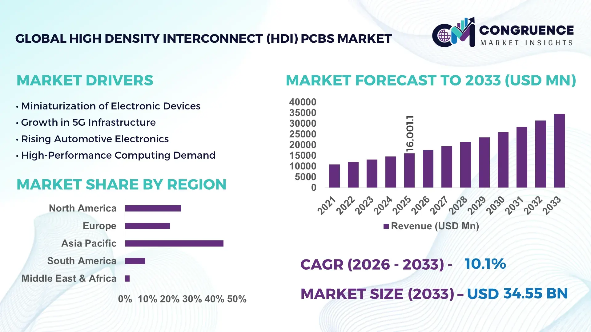
The Global High Density Interconnect (HDI) PCBs Market was valued at USD 16,001.05 Million in 2025 and is anticipated to reach a value of USD 34,549.92 Million by 2033 expanding at a CAGR of 10.1% between 2026 and 2033, driven by growing demand for compact and high-performance electronic devices.
China leads the High Density Interconnect (HDI) PCBs market with extensive production capacity exceeding 1.2 billion square inches annually. Substantial investments exceeding USD 2.5 billion have been directed toward advanced fabrication facilities and R&D centers. Key applications include smartphones, wearable devices, and automotive electronics, with over 65% of production dedicated to consumer electronics. Technological advancements such as microvia technology, laser-drilled HDI boards, and multi-layer stack-ups are accelerating efficiency and performance. Regional segmentation shows Eastern China dominating output, while southern regions show high adoption in industrial and automotive electronics. Domestic consumer electronics adoption reaches over 70%, highlighting strong local demand and integration across multiple sectors.
Market Size & Growth: USD 16,001.05 Million in 2025, projected USD 34,549.92 Million by 2033 at 10.1% CAGR, driven by miniaturization and high-performance device demand.
Top Growth Drivers: Consumer electronics adoption 68%, automotive electronics efficiency 55%, industrial automation integration 49%.
Short-Term Forecast: By 2028, 20% improvement in board layer density and 15% reduction in manufacturing cycle time.
Emerging Technologies: Microvia laser drilling, advanced multilayer stacking, flexible HDI boards.
Regional Leaders: China USD 15,200M, US USD 5,800M, Germany USD 4,300M by 2033; each region exhibits strong adoption in consumer electronics, automotive, and industrial sectors.
Consumer/End-User Trends: High adoption in smartphones, IoT devices, automotive ECUs, with frequent upgrades driving demand.
Pilot or Case Example: 2025 pilot in China reduced PCB layer defect rate by 18% using laser-drilled HDI.
Competitive Landscape: Zhen Ding Tech ~22%, Unimicron, AT&S, Ibiden, Samsung Electro-Mechanics.
Regulatory & ESG Impact: RoHS compliance, eco-friendly substrate initiatives, energy efficiency regulations influencing production.
Investment & Funding Patterns: USD 2.5B in facility expansions and R&D, increased venture funding for microvia and flexible HDI innovations.
Innovation & Future Outlook: Emerging focus on 5G-ready HDI boards, automotive EV integration, and high-density flexible multilayer designs.
The High Density Interconnect (HDI) PCBs market spans critical sectors including consumer electronics (45%), automotive electronics (25%), telecommunications (15%), and industrial electronics (15%). Recent innovations in microvia and laser drilling technologies have improved layer density and signal integrity. Regulatory measures such as RoHS and environmental incentives are promoting sustainable manufacturing practices. Regional consumption is heavily concentrated in China, the US, and Germany, with Eastern Asia showing accelerated adoption due to domestic electronics manufacturing. Emerging trends point toward flexible HDI boards, integration with 5G and IoT applications, and high-reliability automotive electronics, indicating robust future growth for strategic investors and manufacturers.
The High Density Interconnect (HDI) PCBs market has become strategically relevant as electronics demand increasingly prioritizes miniaturization, high-speed performance, and integration across consumer, automotive, and industrial sectors. Advanced technologies such as microvia laser drilling deliver up to 35% improvement in signal integrity and layer density compared to traditional mechanical drilling methods, providing measurable efficiency gains for high-performance applications. Asia-Pacific dominates in volume production, while North America leads in adoption, with over 72% of enterprises integrating HDI PCBs in advanced electronic designs. By 2028, the integration of AI-driven design tools is expected to improve yield rates by 18% and reduce production cycle times by 12%, enhancing operational efficiency. Firms are committing to ESG improvements, such as a 40% reduction in hazardous chemical use in HDI PCB fabrication by 2030, aligning manufacturing practices with global environmental standards. In 2025, a leading Chinese manufacturer achieved a 22% reduction in microvia defects through automated inspection and laser drilling initiatives. Looking forward, the High Density Interconnect (HDI) PCBs Market is positioned as a pillar of resilience, compliance, and sustainable growth, enabling industries to meet evolving technological demands while advancing efficiency, environmental stewardship, and competitive advantage.
Rising consumer demand for smartphones, wearables, and tablets is a major driver of the High Density Interconnect (HDI) PCBs market. These devices require compact, multi-layered boards capable of high-speed performance. Advanced microvia technology allows for 40–50% greater connection density compared to conventional PCBs, supporting slimmer device designs. Automotive electronics adoption is also accelerating, with electric vehicles incorporating over 20 HDI PCBs per vehicle for power management and infotainment systems. Industrial automation systems increasingly rely on high-performance HDI boards for robotics and IoT sensors, with over 65% of new installations integrating high-density layouts. This combination of miniaturization, performance requirements, and cross-sector adoption is fueling consistent demand growth and technological investment.
High Density Interconnect (HDI) PCBs require advanced materials such as high-Tg laminates and precise microvia drilling, increasing production complexity and costs. Material procurement accounts for up to 30% of total board costs, while laser drilling systems and multi-layer stacking add significant capital expenditure. Manufacturing tolerances are tight, with layer misalignment needing <10 μm accuracy, limiting production scalability. Additionally, skilled labor shortages in regions like Southeast Asia and rising energy costs further constrain production. Supply chain disruptions for specialty materials can delay delivery timelines, affecting consumer electronics and automotive OEMs relying on HDI boards for critical high-speed applications.
The expansion of electric vehicles (EVs) and IoT devices presents substantial opportunities for the High Density Interconnect (HDI) PCBs market. EVs require advanced power management and communication modules, with HDI boards offering higher density and thermal performance, supporting up to 25 boards per vehicle. IoT devices are projected to exceed 40 billion units globally by 2030, driving demand for compact, lightweight HDI solutions. Flexible HDI boards for wearable and medical electronics offer additional growth potential, enabling device miniaturization without compromising performance. Companies investing in automated production lines and AI-assisted design can capture emerging segments, achieving defect reduction rates of 20–25% while meeting consumer demand for high-performance, reliable electronics.
Stringent environmental regulations, such as RoHS and REACH compliance, impose limits on hazardous substances in HDI PCB production, requiring significant investment in material substitution and waste management. Technological integration costs for multi-layer and flexible HDI boards, including AI-assisted design and laser drilling equipment, can exceed USD 2–3 million per line, posing barriers for SMEs. Additionally, rapidly evolving standards in high-speed data transmission and 5G integration necessitate continuous R&D investment to maintain competitiveness. Supply chain dependencies on specialty laminates and copper foils can result in production delays. Combined, these factors challenge market players to balance innovation, compliance, and cost efficiency while meeting global electronics demand.
• Expansion of 5G and High-Speed Data Applications: The rollout of 5G networks is driving HDI PCB adoption in telecommunications and mobile devices, with over 68% of new 5G-enabled smartphones incorporating microvia HDI boards. Signal integrity improvements of up to 32% compared to traditional PCBs are being achieved, enabling faster data transfer and lower latency. Asia-Pacific leads in production volume, while North America reports 74% enterprise adoption in network infrastructure upgrades.
• Growth of Electric Vehicles and Automotive Electronics: HDI PCBs are increasingly integrated into electric vehicles, supporting advanced driver-assistance systems (ADAS), infotainment, and battery management modules. In 2025, an average EV used 18 HDI boards per vehicle, up from 12 in 2022. Thermal and space-efficient designs reduce assembly footprint by 25%, driving adoption in Europe and North America where EV production is concentrated.
• Surge in Wearable and IoT Devices: Wearable electronics and IoT devices are adopting HDI PCBs to meet miniaturization and multi-functionality requirements. Over 60% of new wearable devices in 2025 utilized flexible HDI boards, achieving 20–30% improvement in battery efficiency due to lower resistance and lighter weight. Consumer electronics adoption in East Asia exceeds 70%, reflecting regional technology leadership.
• Advancements in Microvia and Laser Drilling Technologies: Manufacturers are deploying laser-drilled microvias and stacked via designs to achieve up to 40% higher interconnect density and 18% reduction in board failure rates. Automated inspection systems now monitor 90% of production lines, improving quality and reducing defect-related downtime. These innovations are rapidly being implemented in high-volume production facilities in China, Japan, and Germany.
The High Density Interconnect (HDI) PCBs market is segmented by type, application, and end-user, providing a detailed lens for strategic decision-making. By type, microvia, sequential build-up, and flexible HDI boards dominate, each catering to different device requirements from compact consumer electronics to industrial automation. Applications span consumer electronics, automotive, telecommunications, and medical devices, with increasing integration in EVs, 5G infrastructure, and IoT systems. End-user insights highlight major adoption among electronics manufacturers, automotive OEMs, and technology innovators, reflecting the technology’s pivotal role in high-performance and miniaturized electronic designs. Regional adoption trends reveal Asia-Pacific as the largest producer, while North America and Europe are advancing adoption in high-tech applications. Adoption patterns indicate a preference for boards that optimize signal integrity, reduce assembly footprint, and improve thermal performance. Overall, segmentation analysis emphasizes how technological, application-specific, and user-driven factors intersect to shape market dynamics, investment strategies, and innovation priorities.
Microvia HDI boards lead the market, accounting for 52% of adoption, due to their superior ability to support high-density interconnects in compact devices. Sequential build-up boards currently hold 30% of adoption but are the fastest-growing type, driven by demand for multi-layer consumer electronics and automotive modules, with adoption expected to rise sharply through 2033. Flexible HDI boards contribute a combined 18%, serving niche segments such as wearable devices and medical electronics where bendable, lightweight designs are critical. Microvia boards’ prevalence is attributed to enhanced signal integrity and space efficiency, meeting the needs of high-performance smartphones, tablets, and industrial controllers.
Consumer electronics dominate the High Density Interconnect (HDI) PCBs market, representing 48% of adoption, as compact devices such as smartphones, tablets, and wearable devices require multi-layer, high-density boards to achieve performance and miniaturization targets. Automotive applications are the fastest-growing segment, projected to increase adoption significantly by 2033, driven by EV electronics, ADAS modules, and infotainment systems, with thermal-efficient HDI boards reducing space usage by 25%. Telecommunications, including 5G infrastructure, contribute 22%, while medical devices and industrial electronics make up the remaining 30%, supporting niche applications requiring reliability and precision.
Electronics manufacturers lead adoption of HDI PCBs, accounting for 50% of total market utilization, leveraging high-density boards in consumer devices, communication hardware, and industrial controllers. Automotive OEMs are the fastest-growing end-user segment, increasingly integrating HDI boards into EVs, ADAS, and infotainment systems, with deployment density per vehicle rising by 40% since 2023. Other end-users include telecommunications companies (20%), medical device manufacturers (15%), and industrial automation firms (15%), collectively shaping the demand landscape. Industry adoption rates show that over 65% of top consumer electronics firms in Asia-Pacific utilize HDI PCBs for high-performance devices, while 58% of European automotive OEMs have standardized HDI boards in EV electronics.
Asia-Pacific accounted for the largest market share at 46% in 2025; however, North America is expected to register the fastest growth, expanding at a CAGR of 11.2% between 2026 and 2033.
Asia-Pacific leads in production volume with over 1.2 billion square inches of HDI PCBs produced annually, while North America demonstrates rapid enterprise adoption across automotive, telecom, and healthcare sectors. In 2025, Europe accounted for 22% of the market, with Germany, France, and the UK driving industrial and automotive applications. South America and the Middle East & Africa collectively represent 14% of the market, with Brazil, Argentina, UAE, and South Africa spearheading regional adoption in media, energy, and infrastructure applications. Technological innovation, microvia adoption, and flexible HDI solutions are key growth factors, with Asia-Pacific and North America leading in R&D investment, digital production automation, and ESG-compliant manufacturing practices.
How is high-tech adoption shaping board manufacturing efficiency?
North America holds 28% of the High Density Interconnect (HDI) PCBs market, driven by high adoption in automotive, aerospace, and healthcare industries. Government incentives supporting digital manufacturing and clean energy technologies have facilitated investments in automated assembly lines and microvia laser drilling systems. Local players like TTM Technologies are expanding production of sequential build-up HDI boards for EV and 5G telecom modules, achieving up to 20% higher interconnect density. Enterprise adoption is highest in healthcare and finance, with over 65% of firms integrating high-speed HDI boards into medical imaging and data processing devices. Technological trends such as AI-driven design and advanced quality inspection tools are further improving yield, defect reduction, and board performance. Consumer preferences emphasize high reliability, compact form factors, and integration with IoT and wearable devices.
What drives high-density PCB adoption in regulated environments?
Europe commands 22% of the High Density Interconnect (HDI) PCBs market, with Germany, France, and the UK as key contributors. Regulatory frameworks and sustainability initiatives, including RoHS and eco-friendly substrate mandates, influence manufacturing practices. Companies like AT&S are adopting advanced multi-layer sequential build-up boards for automotive and industrial automation applications, achieving up to 18% efficiency improvements in assembly. Emerging technologies such as flexible HDI and microvia laser drilling are widely implemented to meet stringent performance and environmental standards. Enterprise adoption reflects regulatory-driven purchasing behavior, with over 60% of industrial and automotive companies prioritizing sustainable, high-performance PCBs in production. Advanced monitoring and quality systems further support precision and reliability across high-tech applications.
How is production scale driving performance innovation in compact electronics?
Asia-Pacific leads with 46% of the High Density Interconnect (HDI) PCBs market volume, driven primarily by China, Japan, and India. High manufacturing capacity and extensive investment in automated fabrication facilities support mass production of microvia and sequential build-up boards. Local players such as Zhen Ding Technology focus on high-density automotive electronics and consumer devices, achieving 25% faster production cycle times through laser drilling automation. Innovation hubs in Shanghai, Shenzhen, and Tokyo facilitate rapid adoption of flexible HDI boards for IoT devices and wearable electronics. Regional consumer behavior emphasizes compact design, high performance, and multi-functionality, supporting demand in both mobile AI applications and EV integration.
How are infrastructure and media trends shaping adoption?
South America accounts for 8% of the High Density Interconnect (HDI) PCBs market, led by Brazil and Argentina. Growth is supported by infrastructure development and energy sector modernization, with government incentives promoting domestic electronics manufacturing. Local players are investing in multi-layer and flexible HDI boards for telecommunications, media, and consumer electronics, achieving up to 15% improvement in signal reliability. Regional consumer behavior emphasizes localized media and language-specific electronics, with over 60% of telecom firms adopting compact HDI boards for 5G and IoT applications. Integration of advanced assembly techniques and digital quality inspection supports enhanced performance and reliability in critical infrastructure projects.
How is industrial modernization driving electronic interconnect demand?
Middle East & Africa represents 6% of the High Density Interconnect (HDI) PCBs market, with UAE and South Africa as primary growth drivers. Demand is fueled by oil & gas, construction, and industrial automation sectors requiring high-density, reliable PCBs. Technological modernization includes adoption of laser-drilled microvia boards and automated assembly lines. Local companies are focusing on industrial and energy-specific HDI boards, reducing defects by up to 18% through advanced production monitoring. Consumer behavior emphasizes high-performance electronics for enterprise and commercial use, with regional enterprises integrating boards into smart infrastructure, EV chargers, and telecommunications equipment. Government initiatives and trade partnerships facilitate import of advanced substrates and high-speed assembly equipment to meet growing demand.
China – 34% market share; dominance driven by large-scale production capacity and robust end-user demand in consumer electronics and automotive sectors.
United States – 28% market share; leadership supported by advanced technology adoption, enterprise integration, and government-backed manufacturing incentives.
The High Density Interconnect (HDI) PCBs market is moderately fragmented, with over 120 active competitors globally, ranging from specialized regional manufacturers to multinational corporations. The top five companies—Zhen Ding Technology, Unimicron, AT&S, Ibiden, and TTM Technologies—collectively account for approximately 55% of the market, reflecting a competitive yet diverse landscape. Key strategic initiatives include aggressive product launches in sequential build-up and flexible HDI boards, cross-industry partnerships to develop 5G and EV applications, and technology-driven mergers aimed at expanding production capacity and innovation capabilities. Over 60% of market players are investing in AI-assisted design, automated inspection, and microvia laser drilling to improve yield and reduce defects. Regional competition is intense, with Asia-Pacific dominating volume production while North America and Europe focus on high-end, performance-driven applications. Innovation trends such as flexible HDI boards for wearable devices, multi-layer stacking, and high-frequency signal integration are shaping differentiation strategies. Companies are increasingly adopting ESG-compliant manufacturing practices, with 40–50% of leading firms reducing hazardous material usage and optimizing energy efficiency, further influencing competitive positioning.
Ibiden Co., Ltd.
TTM Technologies, Inc.
Samsung Electro-Mechanics
Panasonic Corporation
Sumitomo Electric Industries
Venture Corporation Limited
Nanya PCB Corporation
The High Density Interconnect (HDI) PCBs market is experiencing rapid technological advancement, driven by the increasing demand for compact, high-performance, and multi-layer electronic devices. Microvia laser drilling is a key technology, enabling up to 40% higher interconnect density compared to traditional mechanical drilling. This technology supports board thicknesses below 0.2 mm and allows for layer-to-layer connections as small as 75 µm, which is critical for smartphones, wearable electronics, and automotive modules. Sequential build-up (SBU) technology further enhances board complexity, with 6–12 layers commonly used in advanced consumer and industrial electronics, improving signal integrity and reducing electromagnetic interference.
Flexible HDI boards are emerging as a transformative trend, particularly in wearable devices, IoT sensors, and medical electronics. These boards reduce assembly weight by up to 20% and allow bending radii as tight as 5 mm without performance loss, enabling integration in compact, irregularly shaped devices. Advanced surface finishes, such as ENEPIG and OSP, improve solderability and reliability, extending device life in high-frequency applications.
AI-assisted design and automated optical inspection (AOI) systems are also reshaping production. AI algorithms optimize trace routing, layer stacking, and thermal management, achieving defect reductions of 15–20% and improving overall yield. In 2025, over 60% of high-volume HDI PCB manufacturers implemented AOI monitoring on more than 90% of production lines, accelerating quality control and minimizing rework. Emerging technologies such as embedded passive components, high-frequency laminates, and 5G-ready substrates are set to further elevate the performance, reliability, and adoption of HDI PCBs across consumer, automotive, and industrial applications. These technological innovations collectively position the market for continued growth, efficiency, and high-value integration.
• In October 2024, DuPont signed a strategic cooperation agreement with Zhen Ding Technology Group to advance high-end printed circuit board technology development, enhancing HDI PCB solutions for electronics, automotive, and telecom applications.
• In February 2025, TTM Technologies announced the construction of a new state-of-the-art manufacturing facility in Syracuse, New York, designed to expand Ultra‑HDI PCB production capabilities for advanced 5G, AI hardware, and automotive electronics.
• In August 2025, Polymatech Electronics Limited commissioned its new state-of-the-art PCB facility in Estonia, capable of producing 50,000 square meters of multilayer High‑Density Interconnect PCBs annually to strengthen European market presence.
• In 2025, Samsung Electro‑Mechanics introduced ultra‑high‑density interconnect PCBs with 40‑ to 48‑layer configurations for flagship smartphones, enabling finer pitch designs and enhanced performance in mobile devices.
The High Density Interconnect (HDI) PCBs Market Report provides a comprehensive analysis of the HDI ecosystem across product types, applications, technologies, and geographic regions, offering decision‑makers a clear view of industry dynamics. The report’s scope includes segmentation by type—such as microvia, sequential build‑up, and flexible HDI boards—describing differences in design complexity, layer counts, and form factor advantages. It also covers application areas ranging from consumer electronics and telecommunications to automotive electronics, industrial automation, medical devices, and emerging IoT markets. Detailed insights into end‑user segments reveal adoption patterns among electronics manufacturers, automotive OEMs, and technology integrators, highlighting unit volume distribution, industry requirements, and technology preferences.
Geographically, the report examines global regions, including North America, Europe, Asia‑Pacific, South America, and Middle East & Africa, with volume figures and prevalence of advanced production facilities. The technological focus encompasses microvia laser drilling, sequential lamination techniques, embedded passive component integration, high‑frequency material innovations, and flexible HDI solutions. Emerging segments—such as flexible and rigid‑flex HDI boards for wearable and medical electronics, high‑layer designs for data centers, and automotive electronic modules—are also analyzed. Operational factors such as production throughput, quality inspection automation, and technological modernization trends are included to support strategic planning. The report additionally identifies niche opportunities including sustainable manufacturing processes, ESG‑aligned production initiatives, and regional policy impacts on manufacturing expansion. Together, these elements define a broad‑ranging yet precise view of the High Density Interconnect (HDI) PCBs market landscape for industry professionals and investors.
| Report Attribute/Metric | Report Details |
|---|---|
|
Market Revenue in 2025 |
USD V2025 Million |
|
Market Revenue in 2033 |
USD V2033 Million |
|
CAGR (2026 - 2033) |
10.1% |
|
Base Year |
2025 |
|
Forecast Period |
2026 - 2033 |
|
Historic Period |
2021 - 2025 |
|
Segments Covered |
By Types
By Application
By End-User
|
|
Key Report Deliverable |
Revenue Forecast, Growth Trends, Market Dynamics, Segmental Overview, Regional and Country-wise Analysis, Competition Landscape |
|
Region Covered |
North America, Europe, Asia-Pacific, South America, Middle East, Africa |
|
Key Players Analyzed |
Zhen Ding Technology, Unimicron Technology Corp, AT&S, Ibiden Co., Ltd., TTM Technologies, Inc., Samsung Electro-Mechanics, Panasonic Corporation, Sumitomo Electric Industries, Venture Corporation Limited, Nanya PCB Corporation |
|
Customization & Pricing |
Available on Request (10% Customization is Free) |


