
Reports
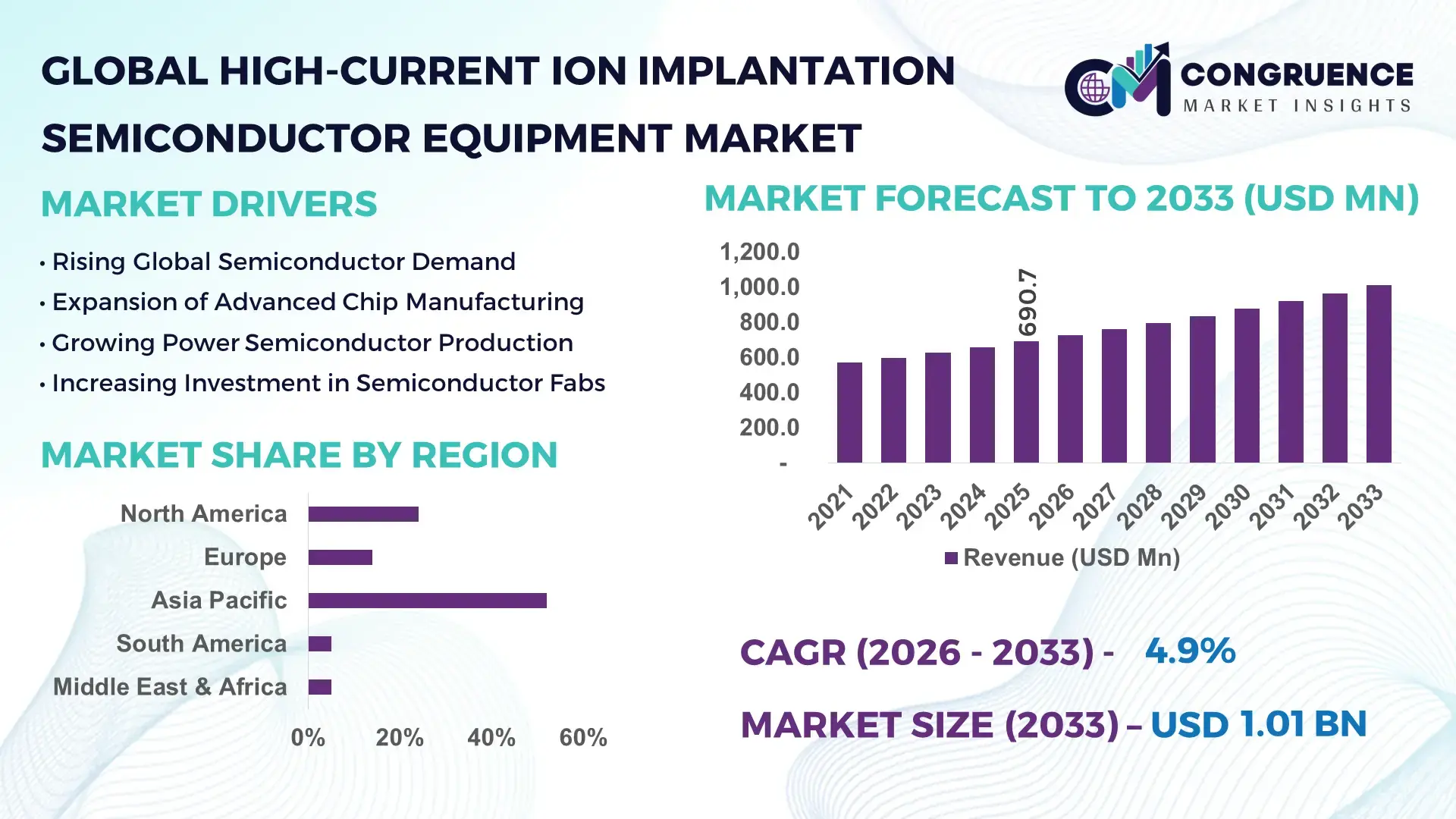
The Global High-Current Ion Implantation Semiconductor Equipment Market was valued at USD 690.7 Million in 2025 and is anticipated to reach a value of USD 1,012.7 Million by 2033 expanding at a CAGR of 4.9% between 2026 and 2033, according to an analysis by Congruence Market Insights. Growth is primarily driven by increasing semiconductor fabrication capacity, advanced chip manufacturing demand, and expanding adoption of high-precision ion implantation systems in logic and memory device production.
Asia Pacific represents the dominant production hub for high-current ion implantation semiconductor equipment deployment due to its massive semiconductor fabrication ecosystem. Countries such as China, Taiwan, South Korea, and Japan collectively host more than 70% of the world’s semiconductor fabrication facilities. Taiwan alone operates over 20 advanced fabrication plants, while South Korea accounts for approximately 60% of global DRAM manufacturing output. China has invested more than USD 150 billion in semiconductor manufacturing expansion programs, with more than 40 new wafer fabrication plants planned or under construction. Additionally, Japan maintains strong equipment manufacturing capabilities, producing around 30% of the world’s semiconductor manufacturing equipment components, supporting widespread adoption of high-current ion implantation systems across advanced chip fabrication processes.
Market Size & Growth: The market stood at USD 690.7 million in 2025 and is projected to reach USD 1,012.7 million by 2033, expanding at 4.9% CAGR, supported by rising semiconductor device complexity and expansion of advanced fabrication nodes.
Top Growth Drivers: Advanced chip node adoption increased by 35%, semiconductor wafer processing demand rose 28%, and power semiconductor device manufacturing expanded 24% globally.
Short-Term Forecast: By 2028, advanced implantation systems are expected to improve dopant precision by 18% and reduce wafer processing variability by 15% in next-generation fabs.
Emerging Technologies: Plasma immersion ion implantation, high-energy beamline implantation systems, and AI-driven process control platforms are improving process efficiency and wafer throughput.
Regional Leaders: Asia Pacific is projected to reach USD 480 million by 2033 driven by large fabrication clusters, North America about USD 260 million supported by advanced node fabs, and Europe nearly USD 150 million through power semiconductor manufacturing expansion.
Consumer/End-User Trends: Semiconductor manufacturers increasingly deploy multi-beam ion implantation systems to handle 300 mm wafer production, now accounting for over 80% of advanced chip manufacturing processes.
Pilot or Case Example: In 2024, a semiconductor fabrication project in South Korea implemented advanced ion implantation control systems achieving 20% reduction in wafer defect rates and 14% improvement in process uniformity.
Competitive Landscape: Applied Materials leads the market with approximately 28% share, followed by Axcelis Technologies, Nissin Ion Equipment, Sumitomo Heavy Industries Ion Technology, and ULVAC.
Regulatory & ESG Impact: Semiconductor equipment manufacturers are adopting energy-efficient implantation systems capable of reducing power consumption by nearly 12% per wafer to align with industry sustainability initiatives.
Investment & Funding Patterns: Global semiconductor fabrication investments exceeded USD 180 billion in the past three years, with a significant portion directed toward advanced manufacturing equipment including ion implantation systems.
Innovation & Future Outlook: Integration of AI-driven defect inspection, precision beam control systems, and automated wafer handling platforms is expected to transform ion implantation efficiency in next-generation semiconductor fabrication.
High-current ion implantation semiconductor equipment plays a critical role in advanced semiconductor fabrication, particularly in logic chips (42% usage), memory devices (33%), and power semiconductors (15%). Innovations in beamline precision and plasma implantation technologies are enabling smaller node architectures below 5 nm. Strong semiconductor manufacturing expansion in Asia Pacific, combined with government incentives in the United States and Europe, continues to accelerate equipment deployment across advanced wafer fabrication facilities.
The High-Current Ion Implantation Semiconductor Equipment Market plays a critical role in enabling advanced semiconductor device manufacturing, particularly as chip architectures move toward sub-5-nanometer nodes and heterogeneous integration. High-current ion implantation systems are essential for doping semiconductor wafers with high precision, enabling controlled electrical characteristics required for modern logic, memory, and power semiconductor devices. As global semiconductor production expands, fabrication plants increasingly rely on advanced beamline ion implantation systems capable of processing over 200 wafers per hour, supporting high-volume manufacturing environments.
Strategically, semiconductor equipment manufacturers are focusing on higher throughput systems and AI-assisted process control to improve yield and minimize defects during implantation. For instance, plasma immersion ion implantation delivers nearly 25% higher uniformity compared to traditional beamline implantation standards, making it increasingly attractive for advanced chip fabrication processes. Such improvements are critical for manufacturers targeting next-generation transistor architectures including gate-all-around (GAA) designs.
Regional dynamics are also shaping the future pathway of the market. Asia Pacific dominates global semiconductor production volume, hosting more than 70% of fabrication facilities, while North America leads in advanced equipment adoption with nearly 45% of enterprises integrating AI-enabled semiconductor manufacturing tools. This technological leadership is supported by major semiconductor initiatives such as large-scale fabrication investments in the United States and Europe.
Short-term technological advancements are expected to significantly improve manufacturing efficiency. By 2028, AI-driven wafer process analytics is expected to reduce implantation-related wafer defects by nearly 18%, improving fabrication yields and lowering manufacturing waste. Additionally, sustainability commitments are influencing equipment design. Semiconductor manufacturers are targeting 15% reductions in equipment energy consumption and up to 20% recycling of process gases by 2030 as part of ESG-aligned manufacturing programs.
Industry micro-scenarios demonstrate the impact of technological innovation. In 2024, a South Korean semiconductor manufacturer achieved a 17% improvement in wafer yield after deploying advanced ion implantation monitoring systems integrated with real-time process analytics. Such results highlight the operational advantages of integrating intelligent equipment technologies within semiconductor fabrication environments.
Looking ahead, the High-Current Ion Implantation Semiconductor Equipment Market will remain a critical pillar supporting the semiconductor ecosystem. Continuous innovation in implantation precision, automation, and sustainability will position this market as a key enabler of resilient semiconductor supply chains, regulatory compliance, and long-term sustainable growth in the global electronics industry.
The High-Current Ion Implantation Semiconductor Equipment Market is influenced by rapid advancements in semiconductor manufacturing technologies, expanding global fabrication capacity, and increasing demand for high-performance computing devices. Ion implantation systems are fundamental in semiconductor fabrication processes, enabling precise control of dopant concentration in silicon wafers used to produce integrated circuits and advanced electronic components. With the semiconductor industry transitioning toward smaller node architectures such as 7 nm, 5 nm, and below, the requirement for high-precision ion implantation tools has increased significantly. Semiconductor manufacturers are also adopting 300 mm wafer production lines, which account for nearly 80% of global wafer output, driving demand for high-throughput implantation systems. In addition, the rising adoption of electric vehicles, artificial intelligence hardware, and 5G infrastructure has accelerated semiconductor production globally. Government initiatives aimed at strengthening domestic semiconductor manufacturing capacity in regions such as the United States, Europe, and Asia are also contributing to increased investments in semiconductor fabrication equipment, including high-current ion implantation systems.
The global expansion of semiconductor fabrication facilities is one of the most significant drivers of demand for high-current ion implantation semiconductor equipment. Semiconductor manufacturing involves multiple implantation steps during wafer processing to precisely modify electrical properties of silicon substrates. As semiconductor devices become more complex, the number of implantation steps required per wafer has increased. Modern logic chip production can involve more than 25 ion implantation steps, compared to fewer than 15 steps in earlier generation devices. Additionally, the transition to 300 mm wafer fabrication lines, which represent approximately 80% of global semiconductor manufacturing capacity, requires advanced ion implantation systems capable of handling high wafer throughput with improved uniformity. Governments worldwide are investing heavily in semiconductor manufacturing expansion. For example, global semiconductor fabrication capacity is expected to exceed 30 million wafer starts per month, creating substantial demand for high-current implantation equipment used in transistor formation and doping processes.
Despite strong demand, the High-Current Ion Implantation Semiconductor Equipment Market faces restraints associated with extremely high equipment costs and complex installation requirements. Advanced ion implantation systems are highly specialized semiconductor manufacturing tools incorporating high-energy particle accelerators, vacuum chambers, beam control systems, and complex automation modules. The cost of installing and calibrating these systems within semiconductor fabrication plants can exceed tens of millions of dollars per system, making them capital-intensive investments. Additionally, semiconductor fabrication facilities require cleanroom environments with contamination levels below 10 particles per cubic meter, significantly increasing installation complexity. Maintenance and operational expertise also present challenges, as these systems require highly trained engineers capable of managing precision beam alignment and wafer handling processes. These technical and financial barriers can slow adoption among smaller semiconductor manufacturers or new fabrication facilities, limiting market penetration despite growing demand for semiconductor devices globally.
Emerging semiconductor technologies present significant opportunities for the High-Current Ion Implantation Semiconductor Equipment Market. The rapid development of advanced transistor architectures such as gate-all-around (GAA) and FinFET designs requires highly precise doping techniques that can only be achieved using sophisticated ion implantation equipment. These technologies are essential for producing high-performance processors used in artificial intelligence, high-performance computing, and data center infrastructure. Furthermore, the growing market for power semiconductors used in electric vehicles and renewable energy systems has increased demand for specialized implantation processes. Silicon carbide (SiC) and gallium nitride (GaN) devices require unique implantation techniques to achieve optimal electrical performance. Electric vehicle production is projected to exceed 40 million units annually by the end of the decade, significantly increasing demand for power semiconductor components and the advanced manufacturing equipment required to produce them.
The High-Current Ion Implantation Semiconductor Equipment Market faces ongoing challenges related to global supply chain disruptions and shortages of highly skilled semiconductor engineers. Ion implantation systems require complex components such as high-energy particle accelerators, vacuum pumps, ion sources, and advanced control electronics. Many of these components rely on specialized manufacturing processes and limited supplier networks. Disruptions in supply chains can delay the production and delivery of critical equipment needed for semiconductor fabrication expansion projects. Additionally, the semiconductor industry faces a shortage of skilled engineers capable of operating and maintaining advanced manufacturing equipment. Industry estimates suggest that the global semiconductor workforce will require over 1 million additional skilled professionals by 2030 to support expanding fabrication capacity. The limited availability of experienced engineers capable of managing complex ion implantation systems can slow equipment deployment and operational efficiency in semiconductor fabrication plants.
Expansion of Advanced Node Semiconductor Manufacturing: The increasing production of advanced semiconductor nodes below 7 nm has intensified demand for high-current ion implantation systems capable of ultra-precise dopant placement. Approximately 65% of new semiconductor fabrication investments announced between 2023 and 2025 are focused on advanced node manufacturing facilities. These fabrication plants require highly controlled implantation processes to support transistor density increases of over 30% per chip generation, significantly increasing demand for advanced implantation technologies.
Growing Adoption of Silicon Carbide Power Semiconductor Manufacturing: Power semiconductor production using silicon carbide (SiC) wafers has grown significantly, with global SiC device manufacturing capacity increasing by over 40% between 2022 and 2025. Ion implantation plays a critical role in doping SiC wafers to create high-efficiency power devices used in electric vehicles and renewable energy systems. Electric vehicle powertrain components now account for nearly 35% of global SiC semiconductor demand, creating new equipment requirements.
Integration of AI-Driven Process Monitoring Systems: Semiconductor manufacturers are increasingly integrating AI-based monitoring platforms into ion implantation equipment to optimize wafer processing conditions. Advanced analytics platforms can analyze thousands of sensor readings during implantation, improving defect detection and process stability. Early implementations have demonstrated up to 18% improvements in wafer yield and nearly 12% reductions in process variability, enabling more efficient semiconductor manufacturing operations.
Increased Deployment of Automated Wafer Handling Systems: Automation is transforming semiconductor manufacturing processes, with automated wafer handling systems now used in more than 75% of high-volume semiconductor fabrication lines. These systems integrate robotic wafer transport, real-time process monitoring, and automated alignment technologies to improve implantation accuracy and throughput. Automation initiatives have demonstrated up to 20% improvements in production efficiency, particularly in large-scale semiconductor fabrication facilities.
The High-Current Ion Implantation Semiconductor Equipment Market is segmented by type, application, and end-user industries, reflecting the diverse requirements of semiconductor fabrication processes. Different types of ion implantation systems are designed to handle specific implantation currents, beam energies, and wafer processing requirements used in integrated circuit manufacturing. Applications range from advanced logic chip production to memory device fabrication and power semiconductor manufacturing. The market also serves multiple end-user groups including integrated device manufacturers (IDMs), semiconductor foundries, and outsourced semiconductor assembly and test providers. Demand for these systems is closely tied to global semiconductor manufacturing capacity expansion and technological advancements in chip architectures. High-current implantation systems are particularly important for high-volume wafer processing environments, where precise dopant control and high throughput are essential for maintaining semiconductor manufacturing efficiency.
High-Current Ion Implantation Semiconductor Equipment can be broadly categorized into High-Current Beamline Ion Implanters, Plasma Immersion Ion Implanters, and Medium-Current Hybrid Implantation Systems. Among these, high-current beamline ion implanters represent the leading equipment type, accounting for approximately 58% of industry adoption, as they are widely used in high-volume semiconductor manufacturing for transistor source and drain doping processes. These systems provide high throughput and precise beam control required for modern semiconductor fabrication facilities operating with 300 mm wafers. Plasma immersion ion implantation systems represent a growing technology category. While their current adoption remains lower at roughly 22% of equipment deployments, these systems are increasingly used in advanced semiconductor manufacturing processes that require uniform doping across complex three-dimensional structures. The segment is also expected to experience the fastest growth with approximately 6.8% annual expansion due to increasing adoption in advanced node chip production. Medium-current hybrid implantation systems and specialized implantation tools collectively account for the remaining 20% of installations, serving niche semiconductor fabrication processes such as compound semiconductor manufacturing and specialty electronic devices.
• In 2024, a major semiconductor research institute demonstrated plasma immersion ion implantation technology enabling uniform doping across 3D semiconductor structures used in advanced gate-all-around transistor prototypes.
Applications of High-Current Ion Implantation Semiconductor Equipment are concentrated across logic device manufacturing, memory device fabrication, and power semiconductor production. Logic chip production represents the largest application segment, accounting for approximately 45% of implantation equipment utilization, as modern processors require multiple doping steps during transistor formation. Advanced computing processors used in artificial intelligence and high-performance computing environments are increasing demand for these systems. Memory device fabrication accounts for approximately 32% of total equipment usage, driven by large-scale production of DRAM and NAND flash memory chips. However, power semiconductor manufacturing is emerging as the fastest-growing application area with about 7.1% annual expansion, largely driven by increasing demand for silicon carbide devices used in electric vehicles and renewable energy systems. Other applications including analog semiconductors and sensor devices contribute the remaining 23% of market usage, particularly in industrial electronics and automotive control systems. In 2025, more than 41% of semiconductor manufacturers reported expanding implantation capacity to support growing demand for high-performance computing processors and advanced automotive semiconductors.
• In 2024, a semiconductor research consortium implemented advanced implantation techniques for silicon carbide wafers used in electric vehicle power modules, improving device efficiency by nearly 12%.
End-users of High-Current Ion Implantation Semiconductor Equipment include semiconductor foundries, integrated device manufacturers (IDMs), and outsourced semiconductor manufacturing providers. Semiconductor foundries represent the leading end-user segment, accounting for approximately 47% of global equipment deployment, as large foundries operate high-volume fabrication facilities producing chips for multiple technology companies. Integrated device manufacturers account for about 35% of equipment utilization, particularly companies that design and manufacture their own semiconductor products such as processors, memory chips, and specialized electronic components. Outsourced semiconductor manufacturing providers and specialized chip fabrication companies collectively represent 18% of installations, supporting niche semiconductor production requirements and regional manufacturing initiatives. The fastest-growing end-user group is semiconductor foundries, expanding at approximately 6.5% annually as global chip demand increases and technology companies outsource manufacturing operations. In 2025, approximately 44% of semiconductor fabrication facilities globally reported adopting advanced ion implantation systems integrated with automated wafer handling platforms to improve manufacturing efficiency.
• In 2024, a large Asian semiconductor foundry deployed next-generation high-current ion implantation equipment integrated with AI-driven process analytics, achieving nearly 15% improvement in wafer processing consistency.
Asia-Pacific accounted for the largest market share at 52% in 2025 however, North America is expected to register the fastest growth, expanding at a CAGR of 5.6% between 2026 and 2033.
Asia-Pacific leads due to its extensive semiconductor manufacturing infrastructure and concentration of wafer fabrication facilities. The region hosts more than 75% of global semiconductor production capacity and over 65% of the world’s 300 mm wafer fabrication plants. China, Taiwan, South Korea, and Japan collectively operate more than 120 semiconductor fabrication facilities, many of which deploy high-current ion implantation systems for transistor doping and advanced device manufacturing. North America follows with approximately 24% of global equipment demand, driven by advanced logic chip manufacturing and large-scale semiconductor investments. Europe represents roughly 14% of the market, supported by strong demand for power semiconductor devices used in electric vehicles and industrial electronics. South America and the Middle East & Africa together account for the remaining 10%, where semiconductor research centers and emerging electronics manufacturing initiatives are gradually increasing equipment adoption. Government-backed semiconductor initiatives across the United States, Europe, and Asia are expected to significantly influence equipment procurement trends, with more than USD 300 billion in semiconductor manufacturing investments announced globally.
North America accounts for approximately 24% of the global High-Current Ion Implantation Semiconductor Equipment Market, driven by strong semiconductor research capabilities and advanced fabrication facilities. The United States leads regional demand, supported by large-scale semiconductor manufacturing investments exceeding USD 50 billion under national semiconductor development programs. The region hosts more than 20 advanced semiconductor fabrication plants, many of which produce high-performance processors and memory devices used in artificial intelligence, cloud computing, and data center infrastructure. The semiconductor sector contributes significantly to equipment demand, particularly for ion implantation systems used in transistor doping and silicon wafer processing. Regulatory initiatives encouraging domestic chip manufacturing are accelerating equipment deployment in new fabrication facilities. Technological transformation is also shaping the market, with advanced fabrication lines integrating AI-driven process monitoring systems capable of improving wafer yield by nearly 15%. A notable industry player, Axcelis Technologies, continues to expand implantation equipment innovation by developing high-throughput systems capable of processing over 200 wafers per hour, strengthening regional manufacturing capabilities. Enterprise adoption patterns in North America show higher deployment across high-performance computing and automotive semiconductor manufacturing.
Europe represents approximately 14% of the global High-Current Ion Implantation Semiconductor Equipment Market, supported by the region’s strong presence in automotive electronics, industrial automation, and power semiconductor manufacturing. Germany, France, and the United Kingdom collectively account for nearly 65% of semiconductor manufacturing activity within Europe, with Germany emerging as the largest manufacturing hub for automotive-grade semiconductor devices. European semiconductor policies emphasize supply chain resilience and domestic chip production, encouraging the expansion of semiconductor fabrication infrastructure. Environmental and sustainability regulations also influence semiconductor equipment development, with manufacturers targeting energy efficiency improvements of up to 20% in semiconductor fabrication processes. Emerging technologies such as silicon carbide and gallium nitride semiconductor devices are gaining traction in Europe’s electric vehicle and renewable energy sectors. A regional industry example includes NXP Semiconductors, which continues to expand its semiconductor manufacturing capabilities to support automotive electronics production. Consumer and enterprise behavior across Europe reflects strong demand for semiconductor devices used in industrial automation systems, smart energy infrastructure, and next-generation electric vehicle power electronics.
Asia-Pacific represents the largest regional market for High-Current Ion Implantation Semiconductor Equipment, accounting for approximately 52% of global equipment deployment. The region hosts the world’s largest semiconductor manufacturing ecosystem, with China, Taiwan, South Korea, and Japan operating more than 120 semiconductor fabrication plants collectively. Taiwan alone produces nearly 60% of the world’s contract semiconductor manufacturing output, while South Korea dominates memory chip manufacturing with approximately 70% of global DRAM production capacity. China has announced semiconductor manufacturing investments exceeding USD 150 billion, with more than 40 new wafer fabrication plants under development or construction. Manufacturing trends in the region focus heavily on advanced node chip production, including 5 nm and 3 nm fabrication technologies, which require highly precise ion implantation equipment. Regional innovation hubs in Taiwan and South Korea continue to lead advancements in semiconductor manufacturing automation. Japanese equipment manufacturer Nissin Ion Equipment is actively developing next-generation implantation systems capable of handling high-current beam applications for advanced semiconductor devices. Consumer behavior across Asia-Pacific reflects strong growth in mobile electronics, artificial intelligence devices, and electric vehicles, all of which drive semiconductor production demand.
South America holds an estimated 5% share of the High-Current Ion Implantation Semiconductor Equipment Market, with Brazil and Argentina emerging as the primary contributors to regional semiconductor activity. Brazil accounts for nearly 60% of semiconductor-related manufacturing output in the region, particularly in consumer electronics assembly and automotive electronics components. Infrastructure expansion and increasing demand for electronic devices have stimulated interest in semiconductor manufacturing capabilities. Government initiatives supporting electronics manufacturing and trade partnerships with global technology companies are encouraging investment in semiconductor research and manufacturing infrastructure. Brazil’s industrial technology programs have allocated funding to support semiconductor development and microelectronics research laboratories. Regional demand is also linked to expanding telecommunications networks and automotive electronics production. Consumer technology adoption trends in South America demonstrate strong growth in smartphones and connected devices, which account for more than 70% of semiconductor component demand in the region, indirectly supporting the need for semiconductor manufacturing equipment including ion implantation systems.
The Middle East & Africa accounts for approximately 5% of the global High-Current Ion Implantation Semiconductor Equipment Market, with demand primarily driven by technology modernization initiatives and increasing investments in electronics manufacturing capabilities. The United Arab Emirates and South Africa are emerging as key regional technology hubs supporting semiconductor research and advanced electronics development. Governments in the region are prioritizing digital transformation initiatives, allocating investments toward semiconductor research centers and technology innovation programs. Infrastructure modernization in telecommunications and energy sectors is increasing the demand for advanced electronic components used in smart grid systems and industrial automation technologies. Regional manufacturing initiatives are also encouraging partnerships with international semiconductor technology providers. Technology adoption trends indicate rising demand for semiconductor-enabled devices across telecommunications networks and smart infrastructure projects. Enterprise technology deployment in the region is growing rapidly, with nearly 45% of large enterprises adopting advanced digital infrastructure platforms, indirectly stimulating demand for semiconductor manufacturing capabilities.
China – 21% Market Share: The leadership is supported by large-scale semiconductor fabrication investments and more than 40 new wafer fabrication facilities under development, strengthening domestic chip production capacity.
United States – 19% Market Share: It maintains a strong position due to advanced semiconductor fabrication plants, significant research investments, and expanding domestic chip manufacturing initiatives.
The High-Current Ion Implantation Semiconductor Equipment Market demonstrates a moderately consolidated competitive structure, characterized by a limited number of specialized equipment manufacturers dominating global supply. Approximately 25–30 active companies participate in the design and manufacturing of semiconductor ion implantation systems, but the top five companies collectively control nearly 68% of the global market due to their advanced technological capabilities and long-standing relationships with semiconductor fabrication plants.
Leading companies compete primarily on technological innovation, throughput capacity, and system precision. High-current ion implantation systems must deliver precise dopant placement across 300 mm wafers, requiring sophisticated beam control technologies, vacuum systems, and advanced wafer handling automation. Equipment manufacturers are increasingly integrating AI-driven process monitoring systems capable of analyzing thousands of process variables in real time, enabling semiconductor manufacturers to reduce defect rates and improve wafer yields.
Strategic collaborations and product innovation represent key competitive strategies. Equipment suppliers are actively working with semiconductor foundries and integrated device manufacturers to develop customized implantation solutions for emerging chip architectures such as gate-all-around transistors and 3D semiconductor structures. Research and development spending among leading companies accounts for nearly 12–15% of annual operating expenditure, highlighting the importance of technological leadership.
Mergers, partnerships, and regional expansion strategies are also shaping competition. Several equipment manufacturers are expanding production facilities in Asia-Pacific to support the region’s large semiconductor manufacturing ecosystem. Continuous innovation in plasma implantation technology, high-energy beamline systems, and automated wafer processing is expected to intensify competition while strengthening technological capabilities across the industry.
Axcelis Technologies, Inc.
ULVAC Technologies, Inc.
Nissin Ion Equipment Co., Ltd.
Sumitomo Heavy Industries Ion Technology Co., Ltd.
Advanced Ion Beam Technology Inc.
Eaton Corporation
High Voltage Engineering Europa B.V.
Plasma-Therm LLC
Scia Systems GmbH
Danfysik A/S
Varian Semiconductor Equipment Associates
Ion Beam Services
Mevion Medical Systems
Hitachi High-Tech Corporation
Technological innovation is a defining characteristic of the High-Current Ion Implantation Semiconductor Equipment Market, as semiconductor manufacturers increasingly demand greater precision, higher throughput, and improved process efficiency in wafer fabrication. High-current ion implantation systems are designed to accelerate ionized dopant atoms toward semiconductor wafers at high velocities, allowing precise control of electrical properties within silicon structures used to build integrated circuits.
Modern high-current ion implanters are capable of delivering beam currents exceeding 20 milliamperes, enabling high-throughput wafer processing in advanced semiconductor fabrication facilities. These systems are widely deployed in 300 mm wafer production lines, which represent more than 80% of global semiconductor manufacturing capacity. Advanced beamline technologies now incorporate multi-angle implantation capabilities, enabling uniform dopant distribution even in complex three-dimensional transistor architectures such as FinFET and gate-all-around designs.
Automation and digital transformation are also influencing technological development. Semiconductor manufacturers are increasingly integrating AI-driven process analytics platforms within implantation systems to monitor beam stability, wafer temperature, and dopant uniformity. These platforms can analyze thousands of sensor data points during implantation cycles, allowing engineers to detect anomalies and optimize manufacturing conditions. Early deployments have demonstrated defect rate reductions of nearly 18% and process stability improvements exceeding 12%.
Plasma immersion ion implantation technology is another emerging innovation gaining traction in advanced semiconductor manufacturing. Unlike conventional beamline implantation systems, plasma immersion techniques allow uniform doping across complex wafer geometries without requiring beam scanning. This capability is particularly valuable for emerging 3D semiconductor structures and advanced power semiconductor devices.
Equipment manufacturers are also investing in energy-efficient implantation systems. Next-generation implanters incorporate optimized vacuum systems and energy recovery modules capable of reducing power consumption per wafer by 10–15%. These technological advancements support semiconductor manufacturers’ sustainability targets while improving operational efficiency in high-volume fabrication environments.
• In February 2026, Axcelis Technologies introduced the Purion H6™ high-current ion implanter, designed for next-generation semiconductor manufacturing. The system integrates enhanced particle control, improved dose accuracy, and Eterna™ ELS7 ion source technology to improve beam stability, productivity, and reliability for advanced logic, memory, and image-sensor devices. Source: www.axcelis.com
• In September 2025, Axcelis Technologies launched the Purion Power Series+™ ion implant platform to support next-generation silicon carbide (SiC) power semiconductor devices. The platform includes new systems such as Purion H200+ SiC, Purion M+ SiC, and Purion EXE+ SiC, enabling higher device performance and productivity for emerging superjunction power electronics.
• In April 2024, Axcelis Technologies announced the shipment of its Purion EXE™ SiC high-energy ion implanter and successful evaluation of the Purion H200™ SiC medium-energy implanter at major power semiconductor manufacturers in Japan. The deployment supports advanced 150 mm silicon carbide wafer processing used in electric vehicle power devices.
• In February 2026, Axcelis Technologies confirmed that it would showcase its latest Purion ion implantation platform, including the new Purion H6 high-current implanter, at SEMICON Korea 2026. The event highlights the company’s latest innovations in implantation technologies designed for advanced semiconductor fabrication nodes.
The High-Current Ion Implantation Semiconductor Equipment Market Report provides a comprehensive analysis of global industry dynamics, technological advancements, and evolving semiconductor manufacturing trends influencing the adoption of ion implantation systems. The report evaluates multiple equipment categories used in semiconductor fabrication, including high-current beamline ion implanters, plasma immersion ion implantation systems, and hybrid implantation technologies designed for specialized semiconductor applications.
The report covers a wide range of semiconductor manufacturing processes where high-current ion implantation equipment is deployed, including logic device fabrication, memory chip production, and power semiconductor manufacturing. These processes involve complex wafer processing operations requiring precise dopant control, particularly in advanced semiconductor nodes below 7 nanometers, where transistor density and performance optimization are critical.
Geographically, the report analyzes market developments across North America, Europe, Asia-Pacific, South America, and the Middle East & Africa, highlighting regional semiconductor manufacturing capacities, technological capabilities, and industry investment patterns. Asia-Pacific remains the largest manufacturing region with more than 120 semiconductor fabrication facilities, while North America and Europe focus on advanced semiconductor research and high-value chip production.
The scope also includes an examination of end-user industries such as semiconductor foundries, integrated device manufacturers, and specialized chip fabrication providers. Market insights within the report address emerging trends including AI-assisted semiconductor manufacturing, automation in wafer processing, advanced transistor architectures, and next-generation power semiconductor technologies. Additionally, the report evaluates technological innovations in beam control systems, plasma implantation techniques, and high-throughput wafer processing platforms that are shaping the future of semiconductor manufacturing equipment.
| Report Attribute / Metric | Details |
|---|---|
| Market Revenue (2025) | USD 690.7 Million |
| Market Revenue (2033) | USD 1,012.7 Million |
| CAGR (2026–2033) | 4.9% |
| Base Year | 2025 |
| Forecast Period | 2026–2033 |
| Historic Period | 2021–2025 |
| Segments Covered |
By Type
By Application
By End-User Insights
|
| Key Report Deliverables | Revenue Forecast; Market Trends; Growth Drivers & Restraints; Technology Insights; Segmentation Analysis; Regional Insights; Competitive Landscape; Regulatory & ESG Overview; Recent Developments |
| Regions Covered | North America; Europe; Asia-Pacific; South America; Middle East & Africa |
| Key Players Analyzed | Applied Materials; Axcelis Technologies, Inc.; ULVAC Technologies, Inc.; Nissin Ion Equipment Co., Ltd.; Sumitomo Heavy Industries Ion Technology Co., Ltd.; Advanced Ion Beam Technology Inc.; Eaton Corporation; High Voltage Engineering Europa B.V.; Plasma-Therm LLC; Scia Systems GmbH; Danfysik A/S; Varian Semiconductor Equipment Associates; Ion Beam Services; Mevion Medical Systems; Hitachi High-Tech Corporation |
| Customization & Pricing | Available on Request (10% Customization Free) |


