
Reports
The Global GaN Semiconductor Devices Market was valued at USD 2821.03 Million in 2025 and is anticipated to reach a value of USD 12374.6 Million by 2033 expanding at a CAGR of 20.3% between 2026 and 2033. Rapid adoption of GaN power transistors in AI data centers, fast chargers, EV power conversion, telecom infrastructure, and high-frequency RF systems is replacing silicon where switching efficiency and power density determine system economics.
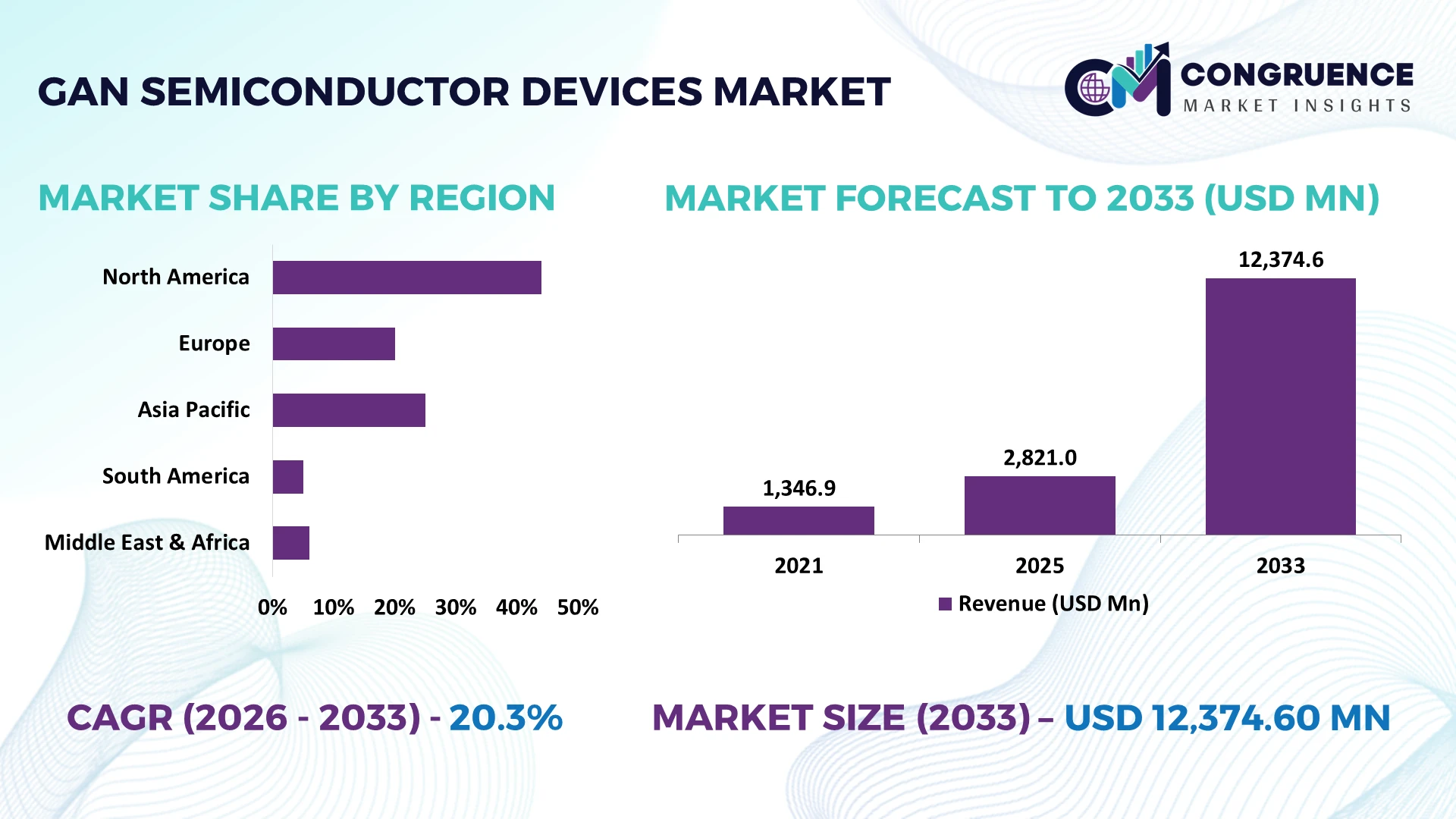
China represents the dominant manufacturing and end-use center, supported by the world’s largest electronics, EV, telecom, and charging-equipment supply chains. China produced about 70% of global electric vehicles in 2024, while its 5G network exceeded 4.25 million base stations by year-end, creating substantial GaN RF and power-device demand. Compared with the United States, China offers greater electronics manufacturing scale, while U.S. suppliers retain strength in high-performance RF and defense applications. Semiconductor trade restrictions are accelerating domestic Chinese compound-semiconductor capacity and supply-chain localization.
Strategically, GaN suppliers need secure wafer capacity, application-specific device portfolios, and geographically diversified packaging partnerships to compete as power and RF architectures migrate beyond silicon.
Market Size & Growth: USD 2,821.03 million in 2025 advances to USD 12,374.6 million by 2033 at 20.3% CAGR, driven by high-frequency power conversion and silicon replacement.
Top Growth Drivers: GaN delivers up to 70% lower switching losses, approximately 40% smaller power systems, and switching frequencies exceeding silicon alternatives by 3–10×.
Short-Term Forecast: By 2028, advanced GaN power designs are positioned to reduce charger size by 30–50% while supporting conversion efficiencies above 95%.
Emerging Technologies: 650-V GaN-on-silicon, bidirectional GaN switches, and integrated GaN power ICs are moving from discrete devices toward compact system-level power architectures.
Regional Leaders: Asia-Pacific approaches USD 6.2 billion, North America USD 3.2 billion, and Europe USD 2.1 billion by 2033, led respectively by electronics scale, data centers, and automotive electrification.
End-User Trends: USB-C power delivery reaching 240 W is expanding GaN adoption beyond smartphones into laptops, monitors, gaming hardware, and compact multiport chargers.
Pilot/Case Example: In 2025, Infineon demonstrated 300-mm GaN wafer technology, targeting 2.3× more chips per wafer than equivalent 200-mm production and materially improving manufacturing economics.
Competitive Landscape: Infineon holds an estimated low-teens global position, competing with Navitas, Power Integrations, NXP, and Texas Instruments across power conversion and integrated GaN architectures.
Regulatory & ESG Impact: GaN power conversion achieving above 95% efficiency can cut conversion losses by 20–40% versus conventional silicon designs, supporting stricter energy-efficiency requirements.
Investment & Funding: Infineon committed €2 billion to its Kulim compound-semiconductor expansion, strengthening high-volume silicon-carbide and GaN manufacturing as supply chains regionalize.
Innovation & Future Outlook: 300-mm manufacturing can provide 2.3× more dies per wafer, shifting competitive advantage toward scalable fabrication, integrated drivers, bidirectional devices, and application-specific GaN platforms.
The GaN Semiconductor Devices Market is increasingly shaped by AI server power supplies, hyperscale data centers, 5G radios, compact USB-C adapters, EV onboard charging, renewable-energy conversion, and aerospace RF systems. GaN transistors can operate at switching frequencies several times higher than conventional silicon devices, enabling smaller magnetics and higher-density power architectures. Recent 300-mm GaN wafer development signals a major manufacturing transition toward improved die economics and scalable production. Semiconductor localization triggered by U.S.–China technology controls is simultaneously reshaping sourcing strategies, creating a strategic foundation for the competitive and investment pathways ahead.
GaN semiconductor devices are becoming strategically critical as AI computing, 5G infrastructure, EV power electronics, robotics, and high-density power supplies push silicon closer to its switching and thermal limits. GaN enables switching frequencies several times higher than silicon while supporting conversion efficiencies above 95%. Semiconductor localization is simultaneously reshaping supply chains as U.S.–China technology controls encourage domestic compound-semiconductor capacity and diversified wafer sourcing.
Technology economics are improving rapidly. Infineon’s transition toward 300-mm GaN wafers can yield approximately 2.3 times more chips per wafer than 200-mm production, materially improving manufacturing efficiency. China leads deployment scale through electronics, telecom, and EV manufacturing, while the United States concentrates innovation in AI infrastructure, RF, aerospace, and advanced power conversion. Europe’s strength remains automotive electrification and industrial power systems.
Through 2028, 650-V GaN, bidirectional switches, integrated power ICs, and 300-mm processing will move deeper into volume applications. AI server power supplies provide a practical deployment case, where GaN reduces conversion losses and power-system footprint. Infineon, Navitas, Power Integrations, and other suppliers are expanding fabrication, packaging, and ecosystem partnerships. Competitive advantage will increasingly depend on wafer economics, system integration, qualification speed, and dependable high-volume supply.
AI data centers are creating an unusually strong GaN adoption trigger because rack power density is moving from conventional 10–20 kW configurations toward 100 kW and beyond for accelerated computing clusters. GaN power devices can deliver switching-loss reductions approaching 50–70% in optimized architectures while enabling power-conversion efficiencies above 95%. The United States leads this transition through hyperscale AI infrastructure investment, where higher rack density makes every conversion loss operationally significant. The shift toward 800-VDC data-center architectures further strengthens high-frequency semiconductor requirements. Infineon, Navitas, Power Integrations, and system partners are consequently developing GaN devices for server PSUs and DC-DC conversion. Strategically, AI infrastructure transforms GaN from a charger-focused technology into a critical data-center efficiency component.
GaN remains structurally more expensive than mature silicon because epitaxy, specialized substrates, wafer processing, packaging, and qualification operate at lower manufacturing scale. Conventional 200-mm GaN fabrication yields fewer devices per wafer, while advanced 300-mm processing can provide approximately 2.3 times more chips. Manufacturing yield differences of even 5–10% materially affect device economics in price-sensitive consumer and industrial applications. U.S.–China semiconductor restrictions also complicate equipment, intellectual-property, and supply-chain planning for Chinese manufacturers. Suppliers are reducing exposure through GaN-on-silicon platforms, foundry diversification, long-term wafer agreements, and larger-diameter fabrication. The critical commercial issue is therefore cost per usable die rather than transistor performance alone; suppliers unable to improve wafer utilization face limited penetration into high-volume mainstream power electronics.
The transition toward 300-mm GaN manufacturing creates an opportunity to move the technology beyond premium applications into mainstream power conversion. A 300-mm wafer provides roughly 2.25 times the surface area of a 200-mm wafer and approximately 2.3 times more chips under comparable designs, spreading processing costs across substantially greater output. Infineon’s 300-mm GaN breakthrough in Austria demonstrates that existing high-volume silicon infrastructure can increasingly support compound-semiconductor manufacturing. Simultaneously, bidirectional GaN switches can replace multiple conventional switching components, reducing component count and simplifying AC-DC power architectures. Companies are investing in larger-wafer R&D, integrated gate drivers, advanced packaging, and foundry partnerships. The non-obvious opportunity is manufacturing compatibility: leveraging depreciated silicon fabs can improve GaN economics faster than building entirely dedicated fabrication networks.
Extracting GaN’s theoretical performance at system level remains difficult because parasitic inductance, thermal interfaces, gate-loop design, electromagnetic interference, and PCB layout become increasingly sensitive as switching frequency rises. GaN devices can switch 3–10 times faster than conventional silicon solutions, but poorly optimized interconnects can eliminate a meaningful portion of that advantage. Junction temperatures commonly approach 150°C in demanding power applications, increasing requirements for thermal design and package reliability. Germany’s automotive sector adds qualification pressure through long validation cycles, high-voltage architectures, and stringent functional reliability requirements. Device manufacturers are responding with integrated drivers, embedded packaging, reference designs, simulation tools, and engineering partnerships with power-system OEMs. Long-term competitiveness depends on converting transistor-level speed into repeatable system efficiency without creating EMI, thermal, or qualification bottlenecks.
Integrated GaN ICs Replace Discretes: Power designers are consolidating GaN switches, drivers, protection, and control functions into integrated devices, cutting parasitic inductance while reducing component counts by roughly 20–40%. Switching frequencies above 1 MHz support smaller magnetics and compact power stages. U.S. suppliers are expanding integrated portfolios and reference designs, allowing charger and server manufacturers to shorten engineering cycles while reducing PCB area and assembly complexity.
Fast Charging Moves Upmarket: GaN charging is shifting from premium smartphone adapters into laptops, gaming hardware, displays, and multiport systems. USB Power Delivery now supports up to 240 W, while GaN architectures commonly deliver efficiencies above 94–95% and approximately 30–50% smaller form factors than legacy silicon adapters. Charger manufacturers are scaling 100–240 W platforms and adopting multi-device integration to serve higher-power consumer electronics.
RF Systems Shift Toward GaN: Telecom and defense equipment manufacturers are replacing legacy RF technologies where power density and frequency performance determine coverage. GaN RF amplifiers can deliver approximately 5–10× higher power density than GaAs alternatives, while efficiencies can exceed 50% in optimized architectures. U.S. defense modernization and satellite deployment are accelerating qualification, prompting semiconductor suppliers to expand GaN-on-SiC portfolios, foundry partnerships, and ruggedized packaging.
Packaging Becomes Performance Lever: Advanced packaging is moving from supporting technology to competitive differentiator as faster switching exposes interconnect losses. Integrated and leadless packages can reduce parasitic inductance by 30–50% versus conventional arrangements while shrinking power-stage footprints. Japanese, European, and U.S. manufacturers are deploying embedded dies, optimized thermal paths, and co-packaged drivers. The non-obvious shift is that packaging engineering increasingly determines usable GaN performance, pushing device companies toward system-level co-design.
GaN Power Devices represent the leading type, accounting for approximately 35–40% of the market, supported by fast chargers, power supplies, renewable-energy converters, industrial systems, and increasingly high-density computing infrastructure. Their advantage stems from high switching frequency, low conduction losses, and compact magnetics compared with conventional silicon architectures. GaN RF Devices retain a mature position in telecom, aerospace, and Defense where high-frequency amplification remains operationally critical, while GaN HEMTs provide the underlying high-electron-mobility architecture for both RF and power applications.
GaN ICs are the fastest-advancing type as manufacturers integrate switches, gate drivers, protection, and sensing into compact packages. Integrated architectures can reduce external component counts by approximately 20–40% and shrink PCB footprints by 30% or more. GaN LEDs remain relevant where efficiency, brightness, and wavelength performance matter, although investment momentum increasingly favors power conversion. Suppliers are consequently directing R&D toward monolithic integration, bidirectional devices, optimized HEMTs, and higher-voltage IC platforms.
Power Conversion is the leading application, representing approximately 30–35% of GaN semiconductor device demand as adapters, industrial power supplies, renewable-energy systems, telecom equipment, and computing infrastructure transition toward higher switching frequencies. GaN conversion stages regularly exceed 95% efficiency in optimized systems, reducing thermal-management requirements while allowing smaller transformers and passive components. Fast Charging is already commercially mature across smartphones and laptops, with USB Power Delivery supporting up to 240 W and accelerating deployment of compact GaN adapters.
Data Centers represent the fastest-growing application as AI computing pushes rack density and power-delivery requirements beyond conventional architectures. GaN switching can reduce power-stage losses by approximately 20–40% in suitable high-frequency designs, making efficiency increasingly valuable across server PSUs and point-of-load conversion. Electric Vehicles are expanding through onboard charging and DC-DC systems, while RF Amplification and Wireless Infrastructure retain strategic importance for high-frequency networks. Suppliers are responding with integrated power ICs, reference designs, higher-voltage devices, and ecosystem partnerships.
Consumer Electronics remains the largest end-user, accounting for approximately 35–40% of GaN semiconductor device demand through smartphone chargers, notebook adapters, displays, gaming equipment, and high-power USB-C accessories. Production scale and short product cycles favor 650-V GaN devices that deliver 30–50% smaller adapter footprints while maintaining conversion efficiencies above 94–95%. Telecom provides an established demand base through RF amplification and wireless infrastructure, while Aerospace and Defense prioritize GaN for radar, electronic warfare, satellite communications, and high-power RF systems where performance outweighs component cost.
Data Centers are emerging as the fastest-growing buyer group as AI accelerator deployment increases power density and conversion requirements. Automotive adoption is simultaneously moving beyond pilot programs into onboard chargers and auxiliary power conversion, while Defense procurement supports specialized GaN-on-SiC architectures. Semiconductor suppliers are targeting these buyers with application-specific devices, integrated drivers, qualification programs, reference platforms, and strategic partnerships rather than standardized portfolios.
Asia-Pacific accounted for the largest market share at 42% in 2025 however, Asia-Pacific is expected to register the fastest growth, expanding at a CAGR of 22.1% between 2026 and 2033.

AI Infrastructure Accelerates High-Density Power Adoption
North America represented approximately 28% of GaN semiconductor device demand in 2025, anchored by AI data centers, aerospace and defense RF systems, fast charging, telecom infrastructure, and advanced power electronics. U.S. hyperscalers are moving toward increasingly dense accelerator clusters, making conversion efficiency and compact power delivery operational priorities. GaN devices exceeding 95% conversion efficiency are gaining relevance in server PSUs and point-of-load architectures, while GaN-on-SiC remains strategically important for radar and electronic warfare. NVIDIA’s transition roadmap toward 800-VDC AI data-center power architecture reinforces demand for higher-frequency power conversion. Navitas, Texas Instruments, Qorvo, and Power Integrations are responding through integrated GaN ICs, reference platforms, packaging improvements, and collaborations with power-system manufacturers.
United States Market Outlook: The United States combines hyperscale computing demand with substantial RF, aerospace, defense, and semiconductor design capability. Domestic data-center electricity consumption is projected to rise sharply through 2030 as AI infrastructure expands. CHIPS-related manufacturing incentives and defense procurement are strengthening local semiconductor ecosystems, while integrated device suppliers increasingly target 650-V GaN power conversion and high-frequency GaN-on-SiC RF applications.
Automotive Electrification Reshapes Power Architectures
Europe accounted for approximately 20% of GaN semiconductor device demand in 2025, with Germany, France, the Netherlands, and Austria concentrating automotive, industrial, telecom, and semiconductor engineering. EV onboard chargers, industrial power supplies, renewable-energy converters, and data-center infrastructure are moving toward higher-frequency architectures that reduce magnetics and cooling requirements. Europe also holds a manufacturing advantage through Infineon’s compound-semiconductor investments and established automotive qualification ecosystems. Infineon’s successful 300-mm GaN wafer processing in Austria represents a major operational shift because the format provides approximately 2.3 times more chips per wafer than 200-mm manufacturing. Suppliers are consequently prioritizing larger-wafer economics, integrated gate drivers, automotive qualification, and local packaging capabilities rather than competing solely through discrete transistor specifications.
Germany Market Outlook: Germany provides Europe’s strongest automotive-industrial demand base, combining premium vehicle engineering, automation, renewable power systems, and established semiconductor research. Battery-electric vehicles represented approximately 17% of German new-car registrations in 2025. This creates a practical pathway for GaN across onboard charging, auxiliary converters, infotainment power supplies, and increasingly compact vehicle electronics requiring higher switching efficiency.
Electronics Scale Drives GaN Commercialization
Asia-Pacific captured approximately 42% of GaN semiconductor device demand in 2025, supported by China’s electronics and EV manufacturing, Taiwan’s semiconductor ecosystem, Japan’s power-device expertise, and South Korea’s consumer-electronics infrastructure. China manufactured roughly three-quarters of global electric cars in 2025 and operates more than 4 million 5G base stations, creating substantial addressable demand across charging, RF amplification, telecom power, and vehicle electronics. Taiwan provides critical foundry and packaging capabilities, while Japan remains influential in GaN materials and power electronics. U.S.–China technology controls are accelerating Chinese localization of epitaxy, fabrication, packaging, and equipment supply. Device manufacturers are expanding domestic product portfolios, qualification programs, and foundry relationships as supply security becomes nearly as important as device efficiency.
China Market Outlook: China combines unmatched electronics assembly scale with EV, charging, telecom, renewable-energy, and consumer-device deployment. Domestic manufacturers benefit from dense downstream ecosystems connecting wafer processing, packaging, charger production, and OEM assembly. More than 16 million electric cars were produced in China during 2025, creating a large platform for future GaN adoption across compact power supplies, onboard electronics, charging equipment, and high-frequency communications hardware.
Digital Infrastructure Expands Power-Efficiency Demand
South America represented approximately 4% of GaN semiconductor device demand in 2025, with Brazil dominating data-center, telecom, renewable-energy, consumer-electronics, and automotive deployment. GaN adoption remains primarily import-dependent because local compound-semiconductor fabrication capacity is limited, making distributor networks, device availability, and system-level engineering important commercial factors. Brazil’s expanding solar generation and cloud infrastructure create demand for compact power conversion, while 5G network rollout strengthens requirements for efficient RF amplification and telecom power supplies. Operators have deployed 5G across all Brazilian state capitals, broadening the installed base for higher-frequency communications equipment. Suppliers are addressing the market through design partnerships, authorized distribution, reference architectures, and relationships with local electronics manufacturers rather than capital-intensive domestic GaN fabrication.
Brazil Market Outlook: Brazil provides the region’s strongest adoption environment through its large telecom subscriber base, expanding data-center footprint, renewable-energy installations, and established vehicle manufacturing industry. Solar capacity has exceeded 50 GW, creating a sizable power-conversion ecosystem where high-frequency semiconductors can improve inverter density and efficiency. Import dependence nevertheless makes technical distribution and dependable inventory critical supplier differentiators.
Digital Investment Creates High-Efficiency Power Demand
Middle East & Africa represented approximately 6% of GaN semiconductor device demand in 2025, with the UAE, Saudi Arabia, Israel, and South Africa providing distinct technology and deployment centers. Saudi Arabia and the UAE are investing heavily in AI computing, cloud infrastructure, telecom modernization, renewable power, and electric mobility, increasing requirements for high-efficiency server power supplies and compact converters. Israel contributes semiconductor design, RF engineering, aerospace, and defense expertise, while South Africa generates demand through telecom and renewable-energy systems. Large solar installations across Gulf economies also strengthen the use case for efficient power conversion under demanding thermal conditions. Semiconductor suppliers are therefore targeting hyperscale operators, telecom vendors, defense integrators, and power-electronics manufacturers through distribution partnerships and application-specific reference platforms.
Saudi Arabia Market Outlook: Saudi Arabia is building a technology-intensive demand base around AI infrastructure, cloud computing, 5G, renewable energy, and industrial digitalization. The Kingdom targets 50% renewable electricity generation by 2030, increasing requirements for efficient inverters and power conversion. Data-center expansion additionally strengthens the commercial case for GaN-based server power architectures capable of reducing conversion losses and equipment footprints.
Infineon, Navitas Semiconductor, Power Integrations, Texas Instruments, NXP, and Qorvo compete across distinct GaN power and RF positions, with integrated-device specialists challenging diversified semiconductor leaders through faster product cycles. The top five suppliers represent approximately 45–50% of addressable GaN device demand. Competition centers on switching efficiency above 95%, 20–40% smaller power-stage footprints, and manufacturing cost reductions enabled by larger wafers. Infineon is scaling 300-mm GaN processing, while Navitas and Power Integrations emphasize integrated power ICs; Qorvo and NXP concentrate heavily on high-performance RF applications. Partnerships with charger, data-center, automotive, and telecom OEMs increasingly determine design wins. Competition is shifting from discrete transistor specifications toward integrated drivers, packaging, reference designs, and assured wafer capacity. Qualification cycles, epitaxial expertise, intellectual property, and fabrication economics create formidable entry barriers. Winning requires manufacturing scale, application-specific integration, dependable supply, system engineering, and customer qualification support across demanding high-frequency platforms.
Infineon Technologies AG
Navitas Semiconductor Corporation
Power Integrations, Inc.
Texas Instruments Incorporated
NXP Semiconductors N.V.
Qorvo, Inc.
STMicroelectronics N.V.
Renesas Electronics Corporation
ROHM Co., Ltd.
Innoscience Technology
Efficient Power Conversion Corporation
Transphorm, Inc.
MACOM Technology Solutions Holdings, Inc.
Wolfspeed, Inc.
Current GaN technology centers on 650 V enhancement-mode HEMTs, integrated gate drivers, and high-frequency power ICs for chargers, server supplies, robotics, and industrial conversion. Optimized GaN stages exceed 95% efficiency, while switching-loss reductions approaching 30% versus silicon MOSFET architectures permit smaller magnetics, cooling systems, and PCB footprints. Adoption is expanding from consumer adapters into higher-power infrastructure as qualification and packaging mature.
Emerging platforms include bidirectional GaN switches, 100 V devices for AI rack conversion, and 300 mm GaN-on-silicon manufacturing. Infineon’s 300 mm process produces approximately 2.3 times more chips per wafer than 200 mm production, improving manufacturing economics. Integrated GaN solutions can switch several times faster than legacy silicon, enabling 20–40% smaller power stages. IDMs with wafer-scale manufacturing and integrated packaging gain cost and supply advantages.
Disruptive development is pushing GaN beyond 650 V toward 1,700 V devices, all-GaN AI power architectures, and monolithic control integration. Navitas has demonstrated 800 V-to-50 V conversion at 98.5% efficiency, while bidirectional GaN enables simplified conversion topologies. Between 2026 and 2028, AI data centers, EV auxiliary systems, robotics, and renewable power will drive qualification. Companies acting now can secure design wins before larger-wafer manufacturing and integrated architectures reset cost, density, and efficiency benchmarks.
September 2024 – Infineon developed the industry’s first 300 mm GaN power wafer using existing silicon manufacturing infrastructure, enabling approximately 2.3 times more chips per wafer than 200 mm processing and establishing a scalable route toward lower-cost high-volume GaN production.
November 2024 – Power Integrations introduced a 1,700 V PowiGaN switch in its InnoMux-2 family, extending GaN beyond earlier 900 V and 1,250 V devices and achieving over 90% efficiency for high-voltage industrial power supplies operating from 1,000 VDC inputs.
May 2025 – Navitas was selected to collaborate with NVIDIA on 800 V HVDC architecture supporting 1 MW AI racks and beyond; the design can reduce copper conductor thickness by up to 45%, strengthening GaN deployment in hyperscale power infrastructure.
February 2026 – Efficient Power Conversion moved its seventh-generation 40 V EPC2366 eGaN transistor into volume production, delivering up to 3 times better performance than comparable silicon MOSFETs and targeting AI server supplies, high-density DC-DC conversion, and advanced motor drives.
The GaN Semiconductor Devices Market Report evaluates GaN RF Devices, GaN Power Devices, GaN HEMTs, GaN ICs, and GaN LEDs across Power Conversion, RF Amplification, Fast Charging, Data Centers, Electric Vehicles, and Wireless Infrastructure. End-user analysis covers Consumer Electronics, Automotive, Telecom, Data Centers, Aerospace, and Defense, capturing the transition from established 650 V power devices toward integrated and higher-voltage GaN architectures.
Regional coverage spans North America, Europe, Asia-Pacific, South America, and Middle East & Africa, examining manufacturing capacity, design ecosystems, deployment intensity, and semiconductor localization. Technology analysis includes 300 mm GaN processing delivering approximately 2.3 times more chips per wafer, bidirectional switches, integrated gate drivers, GaN-on-SiC RF devices, and 1,700 V architectures. The report supports investment planning, fabrication strategy, partnership selection, competitive positioning, application prioritization, and technology-roadmap decisions through 2033.
| Report Attribute/Metric | Report Details |
|---|---|
Market Revenue in 2025 | USD 2821.03 Million |
Market Revenue in 2033 | USD 12374.6 Million |
CAGR (2026 - 2033) | 20.3% |
Base Year | 2025 |
Forecast Period | 2026 - 2033 |
Historic Period | 2021 - 2025 |
Segments Covered | By Type
By Application
By End-User
|
Key Report Deliverable | Revenue Forecast, Growth Trends, Market Dynamics, Segmental Overview, Regional and Country-wise Analysis, Competition Landscape |
Region Covered | North America, Europe, Asia-Pacific, South America, Middle East, Africa |
Key Players Analyzed | Infineon Technologies AG, Navitas Semiconductor Corporation, Power Integrations, Inc., Texas Instruments Incorporated, NXP Semiconductors N.V., Qorvo, Inc., STMicroelectronics N.V., Renesas Electronics Corporation, ROHM Co., Ltd., Innoscience Technology, Efficient Power Conversion Corporation, Transphorm, Inc., MACOM Technology Solutions Holdings, Inc., Wolfspeed, Inc. |
Customization & Pricing | Available on Request (10% Customization is Free) |