
Reports
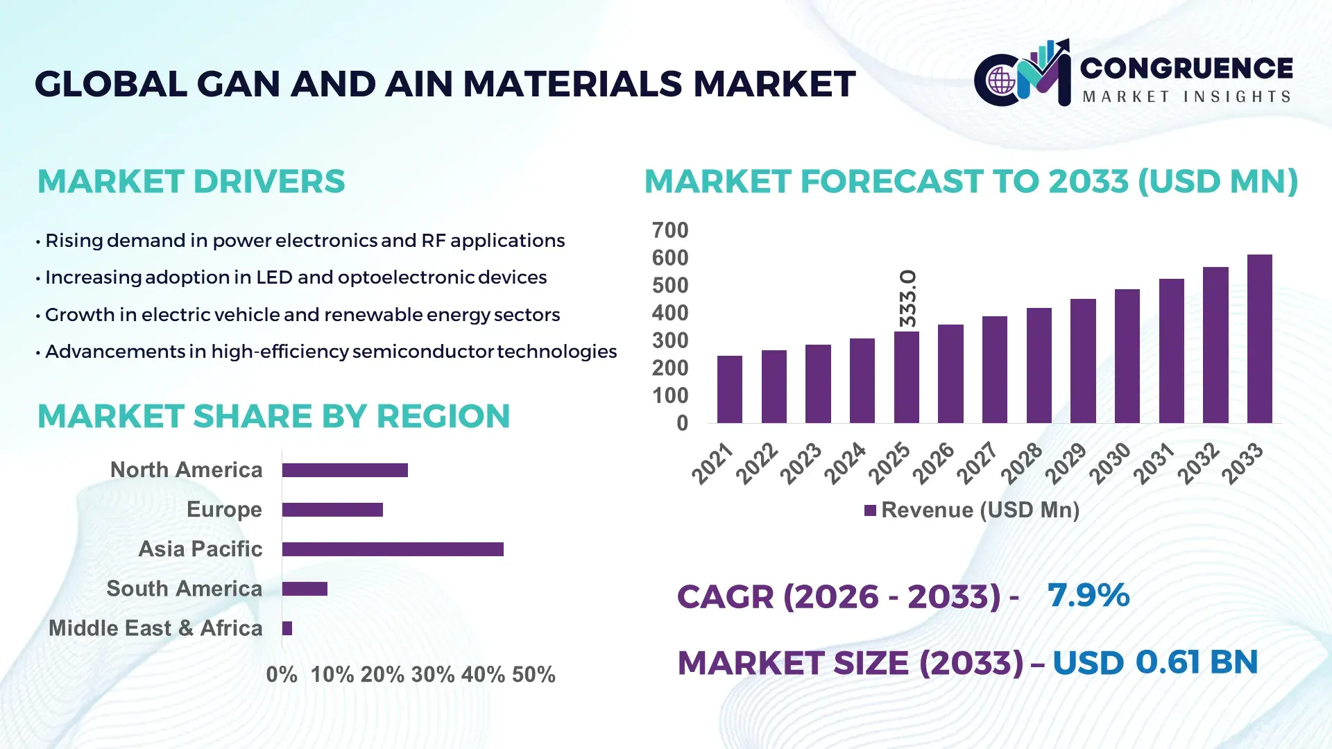
The Global GaN and AIN Materials Market was valued at USD 332.97 Million in 2025 and is anticipated to reach a value of USD 611.75 Million by 2033 expanding at a CAGR of 7.9% between 2026 and 2033. Rising demand for high-efficiency power electronics and next-generation RF devices is accelerating commercial deployment across automotive, telecom, and industrial applications.
China remains a pivotal production hub for GaN and AlN substrates and epitaxial wafers, supported by expanding compound semiconductor fabrication facilities and vertically integrated supply chains. The country operates more than 25 dedicated GaN wafer production lines with cumulative annual capacity exceeding 1.5 million 6-inch equivalent wafers. In 2025, investments in wide-bandgap semiconductor manufacturing surpassed USD 2.3 billion, focused on electric vehicle inverters, 5G base stations, and fast-charging infrastructure. Over 60% of domestic telecom base stations incorporate GaN-based RF components, while high-power LED manufacturing accounts for significant AlN substrate utilization. Continuous advancements in metal-organic chemical vapor deposition (MOCVD) systems and 8-inch GaN-on-silicon wafer scaling are strengthening high-volume manufacturing efficiency and yield optimization across advanced semiconductor clusters.
Market Size & Growth: Valued at USD 332.97 Million in 2025 and projected to reach USD 611.75 Million by 2033, expanding at a CAGR of 7.9% due to increasing adoption of high-frequency GaN power devices and thermally conductive AlN substrates in EV and telecom infrastructure.
Top Growth Drivers: EV powertrain adoption rising by 28%, 5G infrastructure deployment increasing by 24%, and data center power efficiency improvements reaching 18%.
Short-Term Forecast: By 2028, GaN-based power modules are expected to deliver up to 20% system-level energy savings and reduce component footprint by nearly 30% in compact charger applications.
Emerging Technologies: 8-inch GaN-on-silicon wafer scaling, AlN bulk crystal substrate development, and high-electron-mobility transistor (HEMT) optimization for millimeter-wave frequencies.
Regional Leaders: Asia-Pacific projected to reach USD 285 Million by 2033 driven by EV and 5G expansion; North America estimated at USD 165 Million supported by defense and aerospace adoption; Europe forecast at USD 118 Million fueled by industrial automation electrification.
Consumer/End-User Trends: Automotive OEMs, telecom equipment manufacturers, and renewable energy integrators are increasingly integrating GaN power ICs and AlN heat spreaders to enhance thermal performance and compact system design.
Pilot or Case Example: In 2025, a leading EV manufacturer deployed GaN-based onboard chargers achieving 22% weight reduction and 17% efficiency gain under high-load conditions.
Competitive Landscape: Wolfspeed holds approximately 21% share, followed by Qorvo, Sumitomo Electric, Mitsubishi Chemical Group, and TDK Corporation with diversified compound semiconductor portfolios.
Regulatory & ESG Impact: Energy efficiency mandates, carbon neutrality targets, and semiconductor localization incentives are accelerating wide-bandgap material adoption in sustainable power systems.
Investment & Funding Patterns: More than USD 3.5 Billion invested globally between 2024 and 2025 in compound semiconductor fabs, strategic joint ventures, and advanced substrate R&D programs.
Innovation & Future Outlook: Integration of GaN power ICs in AI data centers, hybrid GaN-SiC module architectures, and advanced AlN thermal management solutions are shaping next-generation high-performance electronics.
The GaN and AlN materials market is strategically aligned with high-growth industry sectors including automotive electrification, aerospace and defense radar systems, consumer fast-charging devices, and renewable energy inverters. Automotive applications contribute nearly 35% of overall demand, followed by telecommunications at approximately 27% and industrial power electronics at around 18%. Recent innovations such as low-defect-density AlN substrates, high-voltage enhancement-mode GaN transistors, and advanced epitaxial growth techniques are improving device reliability and thermal conductivity. Stringent energy efficiency standards and global carbon reduction frameworks are encouraging OEMs to transition toward wide-bandgap semiconductors. Asia-Pacific leads consumption due to expanding EV production and 5G rollout, while North America emphasizes defense-grade RF systems and Europe focuses on industrial automation and green energy integration. Increasing R&D in 200mm wafer processing and cost-effective mass production is expected to unlock broader adoption across mainstream electronic platforms.
The GaN and AIN Materials Market holds strategic relevance in the global transition toward high-efficiency power electronics, advanced RF communication systems, and thermal management solutions. As electrification accelerates across automotive, industrial automation, renewable energy, and data center infrastructure, wide-bandgap materials are increasingly replacing conventional silicon-based components. GaN-based power devices deliver up to 40% higher switching efficiency compared to traditional silicon MOSFETs, while AlN substrates offer thermal conductivity exceeding 170 W/mK, significantly outperforming standard alumina ceramics. This performance advantage directly supports compact system design, reduced energy losses, and enhanced reliability in high-voltage applications.
From a regional standpoint, Asia-Pacific dominates in production volume, supported by large-scale wafer fabrication and packaging ecosystems, while North America leads in adoption with nearly 48% of aerospace and defense enterprises integrating GaN RF solutions into next-generation radar and satellite systems. Strategic alliances between material suppliers and EV manufacturers are strengthening vertical integration and securing long-term supply resilience.
By 2028, AI-enabled power management optimization is expected to improve energy efficiency in data centers by approximately 15% through intelligent GaN module integration. ESG commitments are also shaping procurement strategies, with leading semiconductor manufacturers targeting a 30% reduction in Scope 1 and 2 emissions by 2030 through energy-efficient fabrication processes and recyclable substrate initiatives. In 2025, a major U.S.-based semiconductor manufacturer achieved a 19% wafer yield improvement through advanced defect-detection AI systems integrated into GaN epitaxy lines. With expanding regulatory support for energy efficiency and decarbonization, the GaN and AIN Materials Market is positioned as a critical pillar of technological resilience, regulatory compliance, and sustainable industrial growth.
The rapid expansion of electric vehicles and renewable energy systems is significantly driving the GaN and AIN Materials Market. Global EV production exceeded 14 million units in 2025, with increasing integration of GaN-based onboard chargers and power inverters delivering up to 20% higher efficiency and 30% reduced system size compared to silicon alternatives. Solar inverters and energy storage systems are also transitioning to wide-bandgap semiconductors to improve power density and minimize heat losses. AlN substrates are increasingly used in high-power modules due to their superior thermal conductivity, improving device lifespan in demanding grid-scale installations. These measurable efficiency gains and thermal advantages are accelerating industrial-scale material adoption.
Despite strong demand, the GaN and AIN Materials Market faces constraints related to high manufacturing complexity and substantial capital expenditure. Advanced epitaxial growth processes require specialized MOCVD equipment, with single systems costing several million dollars. Defect density control, wafer bow management, and yield optimization remain technical challenges, particularly for larger 8-inch wafers. AlN bulk crystal growth involves slow deposition rates and high-temperature processes exceeding 2000°C, increasing operational energy consumption. Limited availability of high-quality native substrates further restricts scalability. These factors create entry barriers for smaller manufacturers and extend commercialization timelines for next-generation device architectures.
The global rollout of 5G-Advanced networks and hyperscale data centers presents significant opportunities for the GaN and AIN Materials Market. Over 60% of newly deployed macro base stations are incorporating GaN RF amplifiers to enhance signal efficiency and reduce energy consumption. In data centers, power supply units integrating GaN transistors can reduce switching losses by nearly 25%, enabling compact server architectures. Additionally, the rise of AI-driven workloads is increasing demand for efficient power conversion systems capable of handling high computational loads. AlN-based heat spreaders are gaining traction in high-performance computing modules due to their ability to dissipate heat effectively, supporting higher chip densities and sustained operational stability.
Supply chain concentration and material standardization gaps present ongoing challenges for the GaN and AIN Materials Market. A limited number of suppliers dominate high-purity gallium extraction and advanced AlN substrate production, increasing exposure to geopolitical and trade policy fluctuations. In addition, variations in wafer thickness, defect density standards, and packaging compatibility complicate cross-platform integration for device manufacturers. Qualification cycles in automotive and aerospace sectors can exceed 18–24 months, delaying widespread adoption. Furthermore, fluctuations in raw material pricing and energy-intensive production processes contribute to cost volatility, requiring long-term procurement contracts and diversified sourcing strategies to maintain operational stability.
• 200mm GaN Wafer Commercialization Expanding Manufacturing Scale by Over 35%:
The transition from 150mm to 200mm GaN-on-silicon wafers is accelerating large-scale production efficiency across power electronics and RF device fabrication. Manufacturers report up to 35% higher output per production cycle and nearly 20% lower per-device processing cost due to improved wafer utilization. More than 40% of new compound semiconductor fabrication lines commissioned in 2025 are configured for 200mm compatibility. This scaling trend supports higher integration density in electric vehicle inverters and data center power supplies while improving defect control rates by approximately 15% through advanced epitaxial growth optimization.
• GaN Adoption in EV Powertrains Increasing System Efficiency by 18–22%:
Electric vehicle platforms are rapidly integrating GaN-based onboard chargers and DC-DC converters to improve power density and thermal efficiency. Over 30% of newly launched EV models in 2025 incorporated GaN power modules, achieving up to 22% efficiency gains and reducing charger weight by nearly 25%. Switching frequency improvements exceeding 3x compared to silicon-based systems enable smaller passive components and compact architecture. This measurable performance advantage is strengthening GaN penetration across passenger EVs and commercial fleet electrification programs.
• AlN Substrates Enhancing Thermal Conductivity by More Than 40% in High-Power Modules:
Advanced aluminum nitride substrates are increasingly adopted in high-power RF amplifiers and industrial inverters due to superior thermal conductivity exceeding 170 W/mK, representing over 40% improvement compared to traditional alumina ceramics. Approximately 45% of newly developed high-frequency radar modules now utilize AlN heat spreaders to maintain stable operation under elevated temperatures above 200°C. Improved thermal cycling durability has reduced module failure rates by nearly 12%, strengthening reliability benchmarks in aerospace and telecom infrastructure.
• AI-Driven Process Optimization Improving GaN Yield Rates by 15–20%:
Semiconductor fabrication facilities are deploying AI-enabled inspection systems and predictive analytics to enhance GaN epitaxy and wafer processing efficiency. In 2025, over 50% of advanced compound semiconductor fabs implemented machine-learning defect detection, improving wafer yield rates by up to 20% and reducing scrap material by approximately 14%. Automated process control has shortened production cycles by nearly 10%, enabling faster time-to-market for high-frequency communication chips and energy-efficient power devices. This digital transformation is reinforcing operational resilience and production scalability across the GaN and AIN Materials market.
The GaN and AIN Materials Market is segmented by type, application, and end-user industry, reflecting its diversified role across high-performance semiconductor ecosystems. By type, the market primarily includes gallium nitride (GaN) substrates and epitaxial wafers, aluminum nitride (AlN) substrates, and composite or engineered wide-bandgap materials. In terms of application, power electronics represent the largest deployment area, followed by RF and microwave devices, optoelectronics, and thermal management modules. From an end-user perspective, automotive electrification, telecommunications infrastructure, aerospace and defense, consumer electronics, and industrial automation collectively shape demand patterns. Automotive and telecom sectors together account for more than 60% of total material utilization, driven by electrification and high-frequency communication upgrades. Increasing integration of wide-bandgap materials into 5G base stations, EV inverters, and high-density power adapters is reinforcing segmentation-specific growth dynamics across developed and emerging semiconductor manufacturing regions.
Gallium Nitride (GaN) materials currently account for approximately 58% of total adoption in the GaN and AIN Materials Market, supported by their dominant use in high-frequency RF components and high-efficiency power transistors. Aluminum Nitride (AlN) substrates hold nearly 32% share, primarily driven by demand for advanced thermal management solutions in high-power modules. However, high-purity bulk AlN crystal substrates are emerging as the fastest-growing segment, expanding at an estimated CAGR of 9.4% due to increasing deployment in deep-ultraviolet optoelectronics and next-generation radar systems. GaN-on-silicon wafers remain the leading configuration because they enable up to 20% lower manufacturing costs compared to native GaN substrates while maintaining strong electrical performance. Engineered composite substrates and hybrid wide-bandgap materials contribute a combined 10% share, serving niche aerospace and high-temperature industrial applications where thermal stability above 200°C is critical.
Power electronics dominate application demand, accounting for nearly 46% of total GaN and AIN material utilization due to widespread integration in EV inverters, onboard chargers, and renewable energy converters. RF and microwave devices represent approximately 34%, driven by expanding 5G infrastructure and satellite communication systems. However, optoelectronics applications, including UV LEDs and laser diodes, are rising fastest with an estimated CAGR of 10.1%, supported by increasing demand for sterilization systems and advanced sensing technologies. GaN-based high-electron-mobility transistors are replacing silicon LDMOS in telecom amplifiers, delivering up to 25% improved power efficiency at higher frequencies. Thermal management applications using AlN substrates contribute a combined 20% share, particularly in industrial motor drives and high-performance computing modules.
The automotive sector leads end-user adoption with approximately 35% share, driven by integration of GaN power modules in EV powertrains and fast-charging systems. Telecommunications follows with nearly 28% share, supported by mass deployment of GaN RF amplifiers in 5G macro base stations. Aerospace and defense is the fastest-growing end-user segment, expanding at an estimated CAGR of 9.8%, fueled by radar modernization programs and satellite communication upgrades. Industrial automation and renewable energy sectors collectively account for around 22% share, leveraging GaN-based inverters and AlN thermal substrates for energy-efficient motor drives and grid-scale converters. Consumer electronics contributes the remaining 15%, particularly through compact GaN chargers capable of reducing device size by 30% while improving energy efficiency by up to 20%.
Asia-Pacific accounted for the largest market share at 44% in 2025 however, North America is expected to register the fastest growth, expanding at a CAGR of 8.6% between 2026 and 2033.
Asia-Pacific’s dominance is supported by more than 60 operational compound semiconductor fabrication facilities and annual EV production exceeding 14 million units, of which over 35% integrate GaN-based power modules. China and Japan together contribute nearly 70% of regional GaN wafer output, while South Korea accounts for approximately 18% of advanced RF component integration. North America holds around 26% market share, driven by aerospace, defense, and data center modernization, with over 48% of new satellite communication payloads incorporating GaN RF amplifiers. Europe represents nearly 21% share, with Germany, France, and the UK collectively accounting for more than 65% of regional demand due to industrial automation and automotive electrification. South America contributes about 5%, led by Brazil’s expanding renewable energy installations, while the Middle East & Africa region holds close to 4%, supported by telecom upgrades and oil & gas digitalization initiatives. Regional investment in wide-bandgap semiconductor R&D exceeded USD 3.5 billion globally in 2025, reinforcing supply chain localization and next-generation substrate innovation.
How Is Advanced Power Electronics Integration Reshaping Industrial Competitiveness?
North America accounts for approximately 26% of the GaN and AIN Materials Market, supported by strong demand from aerospace, defense, EV manufacturing, and hyperscale data centers. More than 45% of defense radar modernization programs have transitioned toward GaN-based RF modules to enhance signal clarity and reduce energy losses by up to 20%. The region benefits from semiconductor policy incentives allocating over USD 50 billion toward domestic chip fabrication and materials innovation. Technological advancements include rapid deployment of 200mm GaN wafer lines and AI-driven yield optimization systems improving defect detection rates by nearly 18%. Wolfspeed has expanded its silicon carbide and GaN manufacturing capacity in the United States, targeting higher power density modules for EV platforms. Enterprise adoption patterns show higher integration rates within automotive and aerospace sectors, while data center operators prioritize GaN-based power supplies to reduce operational energy consumption by up to 15%.
How Are Sustainability Mandates Accelerating Wide-Bandgap Material Adoption?
Europe represents nearly 21% of the GaN and AIN Materials Market, with Germany, the United Kingdom, and France accounting for over 65% of regional demand. Automotive electrification programs and industrial automation upgrades are central growth pillars, with more than 30% of newly manufactured EV inverters incorporating GaN devices. Sustainability frameworks targeting 55% carbon emission reduction by 2030 are encouraging adoption of energy-efficient power modules. Emerging technologies include GaN-based onboard chargers delivering up to 22% higher efficiency and AlN substrates used in high-frequency rail and grid applications. Infineon Technologies is actively expanding GaN production capabilities within Europe, focusing on high-voltage power transistors for EV and renewable energy markets. Regional procurement behavior emphasizes compliance-driven sourcing, where regulatory pressure encourages manufacturers to prioritize thermally efficient and low-emission semiconductor materials.
What Drives High-Volume Semiconductor Manufacturing and Electrification Momentum?
Asia-Pacific leads the GaN and AIN Materials Market with 44% share and ranks first in production volume, supported by over 60 compound semiconductor fabs. China, Japan, and South Korea are the top consuming countries, collectively accounting for more than 75% of regional utilization. China alone operates over 25 GaN wafer production lines, while Japan remains a leader in high-purity AlN substrate manufacturing. Manufacturing expansion includes 8-inch GaN-on-silicon wafer scaling, improving throughput by approximately 35%. Rapid 5G base station deployment, exceeding 3 million units regionally, supports RF amplifier demand growth of nearly 24% annually. Sumitomo Electric continues investing in advanced AlN crystal growth to enhance thermal conductivity beyond 170 W/mK. Consumer behavior trends reflect strong EV and mobile device adoption, with over 40% of new fast-charging adapters integrating GaN power chips to enable compact design and higher switching efficiency.
How Is Renewable Energy Expansion Influencing Advanced Material Demand?
South America holds close to 5% share of the GaN and AIN Materials Market, with Brazil and Argentina emerging as key contributors. Brazil accounts for nearly 60% of regional demand, primarily driven by renewable energy installations exceeding 30 GW in new solar and wind capacity additions over recent years. Increasing integration of GaN-based inverters is improving energy conversion efficiency by up to 18%. Government incentives supporting clean energy transitions and import tariff adjustments for semiconductor components are strengthening regional procurement. Industrial digitalization initiatives in Argentina’s manufacturing sector are also supporting adoption of thermally stable AlN substrates in high-power equipment. Regional adoption patterns indicate demand tied to energy infrastructure modernization, where reliability and energy efficiency improvements of 15–20% are critical operational drivers.
How Are Infrastructure Modernization and Energy Digitization Stimulating Demand?
The Middle East & Africa region represents approximately 4% of the GaN and AIN Materials Market, with the UAE and South Africa leading regional consumption. Oil and gas digitalization programs are incorporating GaN-based high-frequency sensors and power modules capable of operating above 200°C, improving equipment efficiency by nearly 16%. Telecom infrastructure expansion includes more than 120,000 new 5G base station deployments across major Gulf economies, driving RF amplifier integration. Trade partnerships and semiconductor import facilitation policies are supporting material availability. Local technology integrators are deploying GaN-based power systems in solar installations exceeding 10 GW capacity across the region. Consumer behavior reflects growing demand for energy-efficient infrastructure solutions and advanced communication networks to support smart city initiatives.
China – 31% market share: The GaN and AIN Materials Market in China leads due to large-scale wafer production capacity, strong EV manufacturing output, and extensive 5G infrastructure deployment.
United States – 24% market share: The GaN and AIN Materials Market in the United States is driven by advanced aerospace, defense modernization programs, and expanding domestic semiconductor fabrication investments.
The GaN and AIN Materials market is moderately consolidated, characterized by approximately 25–30 active global competitors specializing in substrate manufacturing, epitaxial wafer growth, and vertically integrated device fabrication, with the top five companies collectively controlling nearly 58% of total market share, reflecting significant technological entry barriers and capital intensity. Competitive positioning is largely driven by 200mm GaN-on-silicon wafer scaling, which improves production throughput by more than 35%, and by advanced aluminum nitride substrates offering thermal conductivity above 170 W/mK, enhancing power module reliability under high-temperature conditions exceeding 200°C. Between 2024 and 2026, more than 12 large-scale fabrication expansion projects were announced globally, targeting higher-volume output for EV powertrains, 5G RF amplifiers, and data center power supplies. Patent filings related to GaN exceeded 1,500 in 2025, underscoring rapid innovation cycles focused on defect-density reduction and high-voltage performance beyond 650V–1200V thresholds. Strategic initiatives include multi-year automotive supply agreements, defense-sector RF modernization contracts, and joint ventures aimed at strengthening regional manufacturing resilience, particularly in Asia-Pacific and North America, where combined public and private semiconductor investments surpassed USD 3.5 billion in 2025, reinforcing competitive intensity and technological differentiation across the GaN and AIN Materials market.
Wolfspeed
Qorvo
Sumitomo Electric Industries
Mitsubishi Chemical Group
Infineon Technologies
TDK Corporation
Nichia Corporation
Fuji Electric
Epistar Corporation
Efficient Power Conversion (EPC)
Transphorm
NXP Semiconductors
Technological advancements in wide-bandgap semiconductor engineering are fundamentally reshaping the GaN and AIN Materials Market, particularly through wafer scaling, epitaxial process optimization, and high-voltage device innovation. The industry is transitioning from 150mm to 200mm GaN-on-silicon wafers, enabling more than 35% higher device output per wafer and approximately 18% improvement in manufacturing efficiency through better edge utilization and defect management. Advanced metal-organic chemical vapor deposition (MOCVD) systems now support tighter thickness uniformity control below ±1.5%, improving device consistency in high-frequency and high-power applications.
In power electronics, enhancement-mode GaN transistors are delivering switching frequencies up to 3x higher than conventional silicon MOSFETs, reducing system energy losses by 15–25% in EV onboard chargers and industrial inverters. High-electron-mobility transistor (HEMT) architectures are being optimized for millimeter-wave frequencies above 30 GHz, supporting next-generation 5G-Advanced and satellite communication platforms.
Aluminum nitride (AlN) substrate technology is also advancing, with bulk crystal growth methods achieving thermal conductivity levels exceeding 170 W/mK and dielectric strength above 15 kV/mm, making them suitable for high-temperature modules operating beyond 200°C. Research into low-defect-density native GaN substrates has reduced threading dislocation density by nearly 20%, improving long-term reliability and device lifespan. Additionally, AI-enabled defect inspection and predictive process analytics are enhancing wafer yield rates by up to 20%, while advanced packaging technologies such as chip-scale integration and double-sided cooling are increasing power density by more than 30%. These technological innovations are strengthening performance benchmarks, improving cost-efficiency, and accelerating commercial deployment across automotive, telecom, aerospace, and renewable energy applications.
• In March 2024, Wolfspeed completed the construction phase of its 200mm silicon carbide and GaN materials fabrication facility in North Carolina, targeting automated production scaling to support EV and industrial power device demand. The facility is designed to significantly expand domestic wide-bandgap wafer output. Source: www.wolfspeed.com
• In February 2025, Infineon Technologies announced volume production of its 300mm GaN wafer technology, becoming one of the first semiconductor manufacturers to implement 300mm GaN processing for power electronics, enabling higher throughput and improved cost efficiency for high-voltage applications. Source: www.infineon.com
• In April 2024, Qorvo expanded its GaN-on-SiC production capacity to meet increasing demand for defense radar and 5G infrastructure, highlighting enhanced RF performance above 30 GHz and improved thermal management in high-power communication systems. Source: www.qorvo.com
• In January 2025, Sumitomo Electric Industries advanced its aluminum nitride substrate manufacturing with improved crystal growth techniques, achieving higher thermal conductivity and supporting next-generation high-frequency modules for automotive and telecom applications. Source: www.sumitomoelectric.com
The GaN and AIN Materials Market Report provides comprehensive coverage of substrate production, epitaxial wafer technologies, and integrated wide-bandgap material applications across multiple high-growth industries. The scope encompasses material types including GaN-on-silicon, GaN-on-SiC, native GaN substrates, bulk aluminum nitride crystals, and engineered thermal management substrates. It evaluates technology evolution from 150mm to 200mm and emerging 300mm wafer processing, alongside advancements in high-electron-mobility transistors, enhancement-mode GaN devices, and high-temperature AlN-based modules operating beyond 200°C.
Geographically, the report analyzes five major regions representing over 95% of global demand, detailing manufacturing clusters, fabrication capacities, and infrastructure deployment metrics such as millions of 5G base stations and multi-gigawatt EV charging networks. Application coverage includes power electronics accounting for nearly 46% of demand, RF and microwave systems at approximately 34%, optoelectronics, aerospace radar modules, industrial automation, and renewable energy inverters.
The report further explores end-user industries including automotive electrification, telecommunications, aerospace and defense, consumer electronics, and industrial equipment manufacturing, identifying adoption rates exceeding 30% in EV powertrain systems and over 40% integration in advanced RF communication payloads. Additional focus areas include supply chain localization trends, wafer yield optimization exceeding 15% through AI-enabled inspection systems, ESG-driven material innovation, and next-generation thermal conductivity benchmarks above 170 W/mK. This structured analysis equips decision-makers with quantitative benchmarks, technology roadmaps, competitive positioning insights, and operational performance indicators essential for strategic planning in the evolving GaN and AIN Materials Market.
| Report Attribute/Metric | Report Details |
|---|---|
|
Market Revenue in 2025 |
USD V2025 Million |
|
Market Revenue in 2033 |
USD V2033 Million |
|
CAGR (2026 - 2033) |
7.9% |
|
Base Year |
2025 |
|
Forecast Period |
2026 - 2033 |
|
Historic Period |
2021 - 2025 |
|
Segments Covered |
By Types
By Application
By End-User
|
|
Key Report Deliverable |
Revenue Forecast, Growth Trends, Market Dynamics, Segmental Overview, Regional and Country-wise Analysis, Competition Landscape |
|
Region Covered |
North America, Europe, Asia-Pacific, South America, Middle East, Africa |
|
Key Players Analyzed |
Wolfspeed, Qorvo, Sumitomo Electric Industries, Mitsubishi Chemical Group, Infineon Technologies, TDK Corporation, Nichia Corporation, Fuji Electric, Epistar Corporation, Efficient Power Conversion (EPC), Transphorm, NXP Semiconductors |
|
Customization & Pricing |
Available on Request (10% Customization is Free) |


