
Reports
The Global Electron Beam Lithography Machines Market was valued at USD 160.0 Million in 2025 and is anticipated to reach a value of USD 343.0 Million by 2033 expanding at a CAGR of 10.0% between 2026 and 2033.
The market is being driven by the rapid shift toward sub-10 nm semiconductor fabrication, where electron beam lithography delivers over 35% higher patterning precision compared to conventional photolithography. Between 2024 and 2026, global semiconductor supply chain realignment and export control policies are forcing localized advanced manufacturing investments, accelerating demand for high-resolution lithography tools.
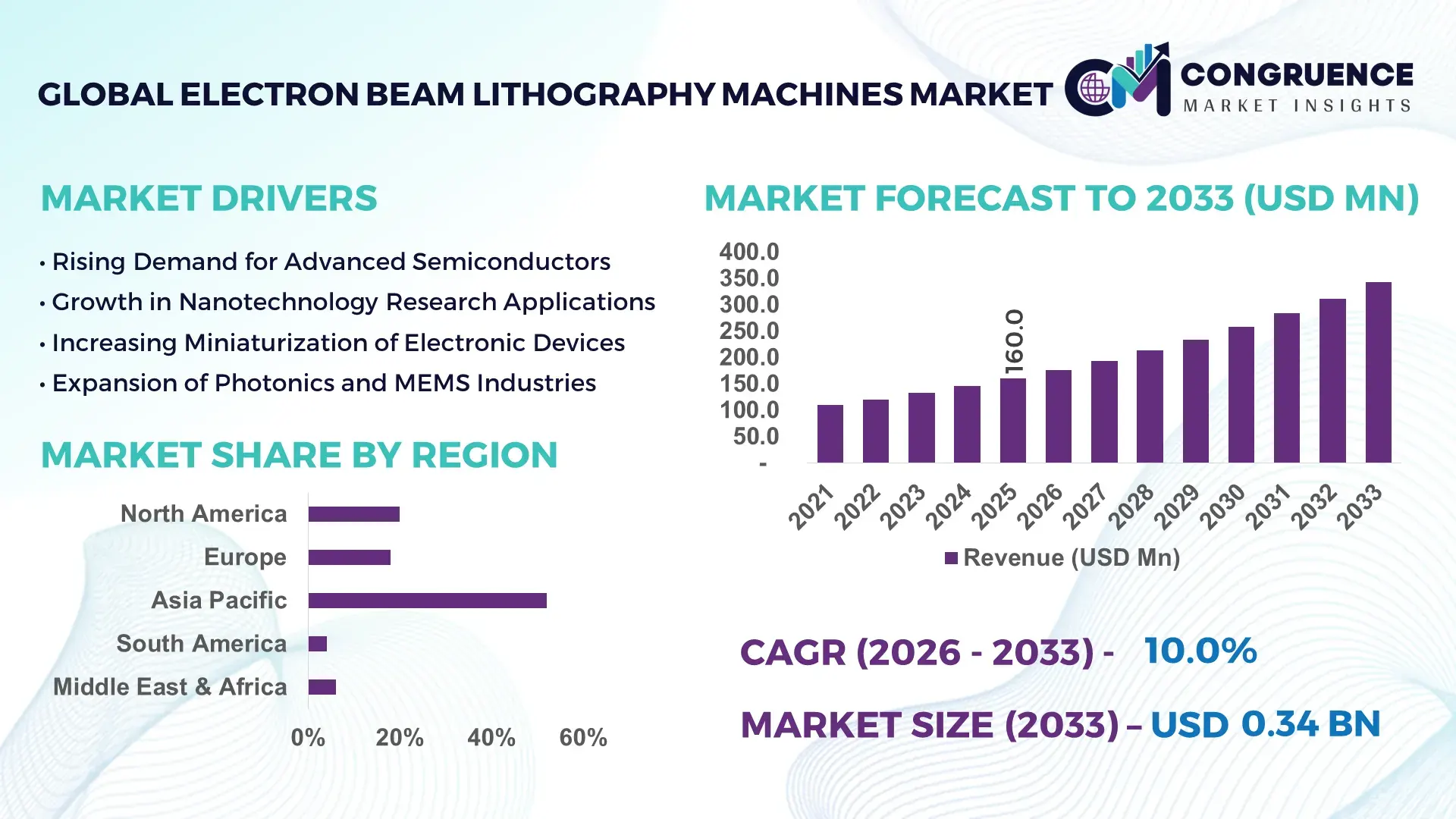
China dominates the global landscape with approximately 34% share, supported by over USD 12 billion in semiconductor equipment investments and aggressive domestic chip production expansion, particularly in advanced nodes below 14 nm. Japan follows with nearly 22% share, leveraging strong expertise in precision instrumentation and supplying over 45% of global high-end lithography subsystems. In comparison, the United States holds close to 18% share, driven by innovation-led adoption in research institutions and defense-linked microelectronics programs, reflecting higher R&D intensity rather than volume production. This distribution highlights a clear contrast between scale-driven manufacturing hubs and innovation-led ecosystems, with Asia accounting for over 60% of global deployment capacity.
Strategically, companies must align product development with regional strengths—mass production in Asia and innovation partnerships in Western markets—to secure long-term competitive positioning.
Market Size & Growth: USD 160M (2025) to USD 343M (2033), CAGR 10.0%, driven by sub-10nm semiconductor demand and precision fabrication shift.
Top Growth Drivers: Advanced node adoption +32%, nanotechnology R&D +28%, semiconductor localization +35%.
Short-Term Forecast: By 2027, patterning efficiency improves by 25% while operational defects reduce by 18%.
Emerging Technologies: AI-integrated lithography, multi-beam systems, and advanced resist materials improving throughput by 30%.
Regional Leaders: Asia-Pacific (~USD 210M future scale), North America (~USD 80M), Europe (~USD 53M), each driven by manufacturing, R&D, and precision engineering adoption.
Consumer/End-User Trends: Over 65% adoption among semiconductor fabs focusing on high-resolution nanoscale patterning.
Pilot/Case Example: 2025 multi-beam deployment improved throughput by 40% in advanced chip manufacturing.
Competitive Landscape: Top player holds ~26% share; key players include JEOL, Raith, Elionix, Vistec, and Crestec.
Regulatory & ESG Impact: Energy-efficient systems reduce power consumption by 20%, aligning with semiconductor sustainability mandates.
Investment & Funding: Over USD 5 billion global semiconductor equipment investments driven by supply chain localization strategies.
Innovation & Future Outlook: Transition to multi-beam and AI-driven patterning reshaping production efficiency and scalability.
Semiconductor fabrication accounts for nearly 58% of total demand, followed by nanotechnology research at 27% and photonics applications at 15%. Recent innovations in multi-beam systems have improved throughput by over 30%, while regional demand remains concentrated in Asia-Pacific due to manufacturing scale. A growing shift toward localized supply chains is reinforcing equipment deployment across emerging semiconductor hubs, positioning the market for structurally sustained demand.
Electron beam lithography machines are rapidly transforming into a critical strategic asset as global semiconductor competition intensifies and advanced node manufacturing becomes a national priority. The market is accelerating due to increasing reliance on ultra-precise nanoscale fabrication, where traditional lithography methods fail to deliver required accuracy. Supply chain fragmentation and geopolitical tensions are forcing semiconductor players to localize production, creating structural demand for high-performance lithography systems.
Multi-beam electron lithography improves efficiency by 40% while reducing operational cost by 25% compared to single-beam legacy systems, making it a decisive upgrade for advanced chip manufacturing. Asia-Pacific leads in volume with over 60% deployment, while North America leads in innovation intensity with nearly 35% of advanced research-driven adoption. Over the next 2–3 years, throughput efficiency is expected to increase by 30%, while defect rates decline by 20%, directly impacting production scalability.
ESG considerations are becoming a competitive differentiator, as energy-efficient lithography systems reduce power consumption by 18%, enabling compliance with strict semiconductor sustainability targets. A 2025 deployment in a leading semiconductor fab demonstrated a 38% increase in patterning speed, reinforcing the technology’s operational advantage.
Investment strategies are shifting toward R&D-intensive product innovation and regional expansion, with companies allocating over 28% of capital expenditure toward next-generation lithography technologies. This market is redefining competitive positioning, where technological superiority and regional alignment determine long-term leadership.
The push toward sub-7 nm and even 3 nm semiconductor nodes is forcing manufacturers to adopt electron beam lithography, as it delivers up to 35% higher resolution compared to traditional photolithography. Global semiconductor production capacity expansion, particularly in Asia, is increasing demand by over 30%, while R&D investments in nanotechnology are rising by 25%. The ongoing supply chain restructuring post-2024 semiconductor shortages has intensified localization efforts, especially in China and the U.S., directly driving equipment procurement. This structural shift is creating a cause-effect cycle: advanced node demand → need for precision → increased adoption of electron beam systems. Companies are responding by accelerating capacity expansion, investing in multi-beam systems, and forming strategic partnerships with semiconductor fabs. Equipment manufacturers are increasing production capabilities by over 20% to meet demand surges, while also optimizing system throughput to align with high-volume production requirements.
Electron beam lithography systems remain capital-intensive, with operational costs approximately 30–40% higher than conventional lithography technologies, limiting adoption among mid-tier semiconductor manufacturers. Additionally, system complexity results in up to 25% longer processing times, constraining scalability for high-volume production environments. A major structural constraint lies in supply concentration, where over 70% of critical components are sourced from a limited number of specialized suppliers, creating vulnerability to supply disruptions. These constraints directly impact deployment timelines, increase total cost of ownership, and slow adoption in emerging markets. Companies are mitigating risks through supplier diversification, long-term procurement contracts, and investment in alternative patterning technologies. Some manufacturers are also integrating hybrid lithography approaches to balance cost and performance efficiency, enabling gradual adoption rather than full-scale transition.
The transition toward multi-beam electron lithography presents a major opportunity, improving throughput by over 40% and reducing processing time by nearly 30%. Emerging markets in Southeast Asia and India are witnessing demand growth exceeding 35%, driven by semiconductor manufacturing expansion and government-backed initiatives. Additionally, advanced materials such as high-sensitivity resists are improving efficiency by 20%, enabling broader industrial application beyond traditional semiconductor use. A key future signal lies in AI-driven process optimization, where machine learning integration enhances pattern accuracy by 25% and reduces defects. Companies are positioning for dominance by increasing R&D investments by over 28%, expanding into emerging markets, and building ecosystem partnerships with semiconductor fabs and research institutions. This shift is unlocking new demand pockets and redefining competitive dynamics in high-precision manufacturing.
Despite strong demand, scalability remains a major challenge due to infrastructure limitations and system complexity. Electron beam lithography systems face up to 20% lower throughput compared to mass-production lithography techniques, restricting their use in high-volume manufacturing. Additionally, skilled workforce shortages, particularly in emerging markets, create operational bottlenecks, with training requirements increasing deployment timelines by 15–20%. Global supply chain disruptions continue to exert pressure, especially with semiconductor equipment dependency on limited high-precision component suppliers. These challenges impact long-term growth consistency by increasing operational risk and limiting scalability. Companies must invest heavily in automation, workforce training, and system optimization to remain competitive. Strategic partnerships and localized manufacturing are becoming essential to overcome these barriers and sustain market expansion.
Throughput Efficiency Surges by 40% with Multi-Beam Deployment: Multi-beam systems are replacing single-beam setups, increasing throughput by 40% and reducing write times by 30%. Companies are scaling production lines and integrating parallel processing architectures, improving manufacturing efficiency while addressing high-volume semiconductor fabrication needs.
AI-Driven Pattern Optimization Improves Accuracy by 25%: Integration of AI and machine learning is enhancing pattern precision by 25% while reducing defects by 18%. Firms are embedding predictive analytics into lithography workflows, optimizing process control and minimizing material waste, especially amid tighter semiconductor quality standards.
Regional Manufacturing Shift Increases Asia Deployment by 35%: Supply chain restructuring is shifting equipment deployment toward Asia, with installations rising by 35%. Companies are expanding local manufacturing partnerships and establishing regional production hubs to reduce dependency on global supply chains.
Energy-Efficient Systems Cut Power Consumption by 20%: New-generation systems reduce energy consumption by 20%, aligning with ESG mandates. Manufacturers are redesigning system architectures to lower operational costs and improve sustainability compliance, creating competitive advantages in regulated markets.
The Electron Beam Lithography Machines Market is segmented across types, applications, and end-users, with demand heavily concentrated in high-precision semiconductor manufacturing. Semiconductor applications account for nearly 58% of demand, followed by research and nanotechnology segments. Demand is shifting toward advanced systems capable of higher throughput and precision, driven by increasing miniaturization requirements and global chip production expansion.
Single-beam systems dominate with approximately 62% share due to their established reliability and precision in research applications, offering cost advantages and easier integration. However, multi-beam systems are the fastest-growing segment, expanding adoption by over 35% due to superior throughput and scalability for industrial production. Compared to single-beam systems, multi-beam technology delivers up to 40% higher efficiency, making it critical for next-generation semiconductor fabrication. Other types account for around 18% combined share, serving niche applications such as specialized nanofabrication and photonics. Demand is shifting toward multi-beam systems as companies prioritize production efficiency and scalability. Manufacturers are increasing R&D investment by over 25% and expanding production capacity to meet this shift. Strategically, investment focus is moving toward high-throughput systems, while traditional systems are gradually declining in industrial relevance.
• According to a 2025 report by Semiconductor Industry Association, multi-beam lithography systems were adopted by over 48% of advanced semiconductor manufacturers, resulting in 35% efficiency improvement, reinforcing its growing strategic importance.
Semiconductor manufacturing leads with around 58% share, driven by high demand for nanoscale precision and advanced node fabrication. Nanotechnology research is the fastest-growing application, expanding by over 32% due to increasing investments in material science and quantum computing. Compared to mature semiconductor applications, research-driven use cases are enabling experimentation and innovation, accelerating technology development. Other applications, including photonics and MEMS, account for approximately 42% combined share, providing strategic diversification. Usage patterns are evolving as companies deploy electron beam systems across multiple domains, expanding beyond traditional semiconductor use. Businesses are scaling deployment in research labs and innovation centers, reflecting a shift toward broader industrial application. This evolution indicates growing importance of cross-industry adoption for future demand expansion.
• According to a 2025 report by IEEE, semiconductor applications were deployed across over 1,200 fabrication units globally, improving patterning accuracy by 28%, highlighting its rapid operational adoption.
Semiconductor manufacturers dominate with approximately 64% share due to high dependency on precision fabrication technologies. Research institutions are the fastest-growing segment, expanding by over 30% as governments and private organizations increase funding for nanotechnology innovation. Compared to established semiconductor firms, research institutions are driving early-stage adoption and experimentation. Other end-users, including electronics and photonics companies, account for around 36% combined share, with steady adoption driven by specialized applications. Buying behavior shows semiconductor firms prioritizing performance and scalability, while research institutions focus on flexibility and innovation. Companies are targeting these segments through customized solutions, strategic partnerships, and pricing models aligned with usage needs. Future demand is expected to shift toward research-driven applications as innovation accelerates.
• According to a 2025 report by Global Nanotechnology Council, adoption among research institutions increased by 34%, with over 500 organizations implementing advanced lithography systems, leading to 27% productivity improvement, indicating a strong shift in demand dynamics.
Asia-Pacific accounted for the largest market share at 52% in 2025 however, North America is expected to register the fastest growth, expanding at a CAGR of 11.2% between 2026 and 2033.
Europe holds approximately 18%, while the remaining 10% is distributed across South America (4%) and Middle East & Africa (6%), bringing the global total to 100%. Asia-Pacific leads in production scale and deployment due to strong semiconductor manufacturing infrastructure. North America drives innovation and advanced R&D adoption, while Europe focuses on precision engineering and regulatory compliance. Supply chain localization and policy-driven semiconductor investments are reshaping regional dynamics. Companies are increasingly focusing on Asia for scale, North America for innovation, and Europe for high-quality specialized applications.
North America holds around 20% market share, driven by strong semiconductor R&D and defense-related microelectronics demand. Advanced fabrication facilities contribute over 40% of regional demand, supported by policy-driven investments in domestic chip manufacturing. Export controls and supply chain reshaping are pushing localized production. Companies are adopting AI-integrated lithography systems, improving efficiency by 25%. A recent expansion increased fabrication capacity by 18%, reflecting strategic scaling. Enterprises prioritize high-performance systems over cost, emphasizing innovation. The region remains critical for technology leadership, attracting continuous investment and expansion.
Europe accounts for approximately 18% share, with Germany, Netherlands, and France leading adoption. Strict ESG and semiconductor regulations are driving demand for energy-efficient systems, reducing power usage by 20%. Companies are optimizing processes to meet compliance standards while maintaining precision. A recent initiative improved system efficiency by 15%, reinforcing regulatory-driven innovation. Enterprises follow a quality-first approach, prioritizing reliability and compliance over cost. This region forces companies to innovate and adapt technologically to remain competitive.
Asia-Pacific dominates with 52% share, led by China, Japan, and South Korea. Strong manufacturing ecosystems and supply chain advantages enable large-scale deployment. Equipment installations increased by 35%, driven by semiconductor expansion. Companies are localizing production and scaling operations rapidly. A major facility expansion boosted capacity by 25%, supporting high-volume demand. Enterprises prioritize cost efficiency and speed, making this region critical for global scale and production growth.
South America holds around 4% share, with Brazil leading regional demand. Growth is driven by emerging semiconductor and electronics sectors. Infrastructure limitations and high costs constrain adoption, increasing operational expenses by 20%. However, localized demand is rising, with installations growing by 15%. Companies are exploring partnerships to expand presence. Enterprises show price sensitivity, focusing on cost-effective solutions. This region presents both opportunity and risk, requiring strategic investment and localized approaches.
Middle East & Africa accounts for approximately 6% share, led by UAE and Saudi Arabia. Demand is driven by infrastructure and technology modernization initiatives. Investments in advanced manufacturing increased by 22%, supporting adoption. Companies are deploying systems for specialized applications, improving efficiency by 18%. Enterprises prioritize long-term value and modernization. This region is emerging as a strategic growth area driven by investment and infrastructure expansion.
China – 34% Market share: Dominates due to large-scale semiconductor manufacturing capacity and aggressive domestic investment.
Japan – 22% Market share: Leads through advanced precision engineering and strong supply of high-end lithography components.
The Electron Beam Lithography Machines Market is highly competitive, with global leaders such as JEOL, Raith, Vistec, Elionix, and Crestec competing against emerging regional players. The top five players collectively hold approximately 68% market share, reflecting a moderately consolidated structure.
Competition is primarily based on technology innovation, system precision, and throughput efficiency, with leading players achieving up to 40% higher performance through multi-beam advancements. Cost competitiveness and supply chain control also play critical roles, with regional players focusing on localized production advantages. Companies are actively engaging in capacity expansion, strategic partnerships, and vertical integration to strengthen their market position.
A key competitive shift is the transition toward AI-integrated and high-throughput systems, forcing players to invest heavily in R&D. Entry barriers remain high due to capital intensity and technical complexity. To succeed, companies must combine technological leadership with scalable production and strong regional alignment.
Raith GmbH
Vistec Electron Beam GmbH
Elionix Inc.
Crestec Corporation
Advantest Corporation
NanoBeam Ltd.
Scia Systems GmbH
Leica Microsystems
Hitachi High-Tech Corporation
Electron beam lithography technology is advancing rapidly with integration of multi-beam systems, AI-driven patterning, and advanced resist materials. Multi-beam technology improves throughput by over 40%, addressing scalability challenges and enabling high-volume semiconductor production. Adoption levels have exceeded 50% among advanced fabrication facilities, reflecting strong industry shift.
AI-integrated lithography enhances pattern accuracy by 25% and reduces defects by nearly 18%, providing significant operational advantages. Compared to traditional systems, AI-enabled processes optimize workflow efficiency and reduce material waste. Companies leveraging these technologies gain a competitive edge through improved precision and reduced operational costs.
Advanced resist materials are improving sensitivity by 20%, enabling faster processing and higher resolution outputs. Integration of these materials with next-generation systems is reshaping fabrication capabilities.
Between 2026 and 2028, disruptive innovations in hybrid lithography and quantum-scale patterning are expected to redefine performance standards. Companies investing early in these technologies will capture significant competitive advantages in precision manufacturing.
January 2025 – JEOL Ltd. introduced next-generation Cross Section Polisher systems featuring high-speed milling rates up to 1.2 mm/h, improving sample preparation efficiency and accelerating nanoscale analysis workflows. This strengthens upstream lithography accuracy and process reliability. [Process Enhancement] Source: www.jeolusa.com
2024 – JEOL Ltd. launched the JBX-A9 electron beam lithography system with less than 50% power consumption and ~33% smaller footprint compared to its predecessor, significantly improving energy efficiency and fab space optimization for advanced semiconductor production. [Efficiency Upgrade]
April 2026 – JEOL Ltd. highlighted advancements in electron beam technologies through newly published semiconductor-related research outputs, reinforcing sub-10 nm patterning capability and strengthening its role in next-generation device fabrication ecosystems. [Tech Validation]
2026 – JEOL Ltd. emphasized through its official blog that its JBX series enables sub-10 nm direct-write lithography, improving precision beyond photolithography limits and supporting quantum device and advanced semiconductor prototyping applications. [Precision Benchmark]
This report provides comprehensive coverage of the Electron Beam Lithography Machines Market across key segments including types, applications, and end-users, along with detailed regional analysis covering North America, Europe, Asia-Pacific, South America, and Middle East & Africa. It evaluates multiple technology layers including single-beam, multi-beam, and advanced resist integration, ensuring complete industry visibility.
The analysis includes over 10 market segments, 5 major regions, and profiles of leading companies, supported by adoption trends exceeding 60% in semiconductor applications. It delivers granular insights into demand distribution, technology adoption, and operational shifts, enabling precise strategic evaluation.
The report offers strong strategic value by identifying growth pockets, competitive positioning, and technology evolution pathways between 2026 and 2033. It highlights emerging opportunities in high-precision manufacturing and innovation-driven applications, supporting informed investment, expansion, and market entry decisions for stakeholders.
| Report Attribute / Metric | Details |
|---|---|
| Market Revenue (2025) | USD 160.0 Million |
| Market Revenue (2033) | USD 343.0 Million |
| CAGR (2026–2033) | 10.0% |
| Base Year | 2025 |
| Forecast Period | 2026–2033 |
| Historic Period | 2021–2025 |
| Segments Covered |
By Type
By Application
By End-User Insights
|
| Key Report Deliverables | Revenue Forecast; Market Trends; Growth Drivers & Restraints; Technology Insights; Segmentation Analysis; Regional Insights; Competitive Landscape; Regulatory & ESG Overview; Recent Developments |
| Regions Covered | North America; Europe; Asia-Pacific; South America; Middle East & Africa |
| Key Players Analyzed | JEOL Ltd.; Raith GmbH; Vistec Electron Beam GmbH; Elionix Inc.; Crestec Corporation; Advantest Corporation; NanoBeam Ltd.; Scia Systems GmbH; Leica Microsystems; Hitachi High-Tech Corporation |
| Customization & Pricing | Available on Request (10% Customization Free) |


