
Reports
The Global CVD SiC Market was valued at USD 850.3 Million in 2025 and is anticipated to reach a value of USD 1,706.8 Million by 2033 expanding at a CAGR of 9.1% between 2026 and 2033. Growth is being driven by conductor-grade thermal components, SiC wafer processing, high-temperature epitaxy, and increasing adoption of ultra-high-purity CVD SiC coatings.
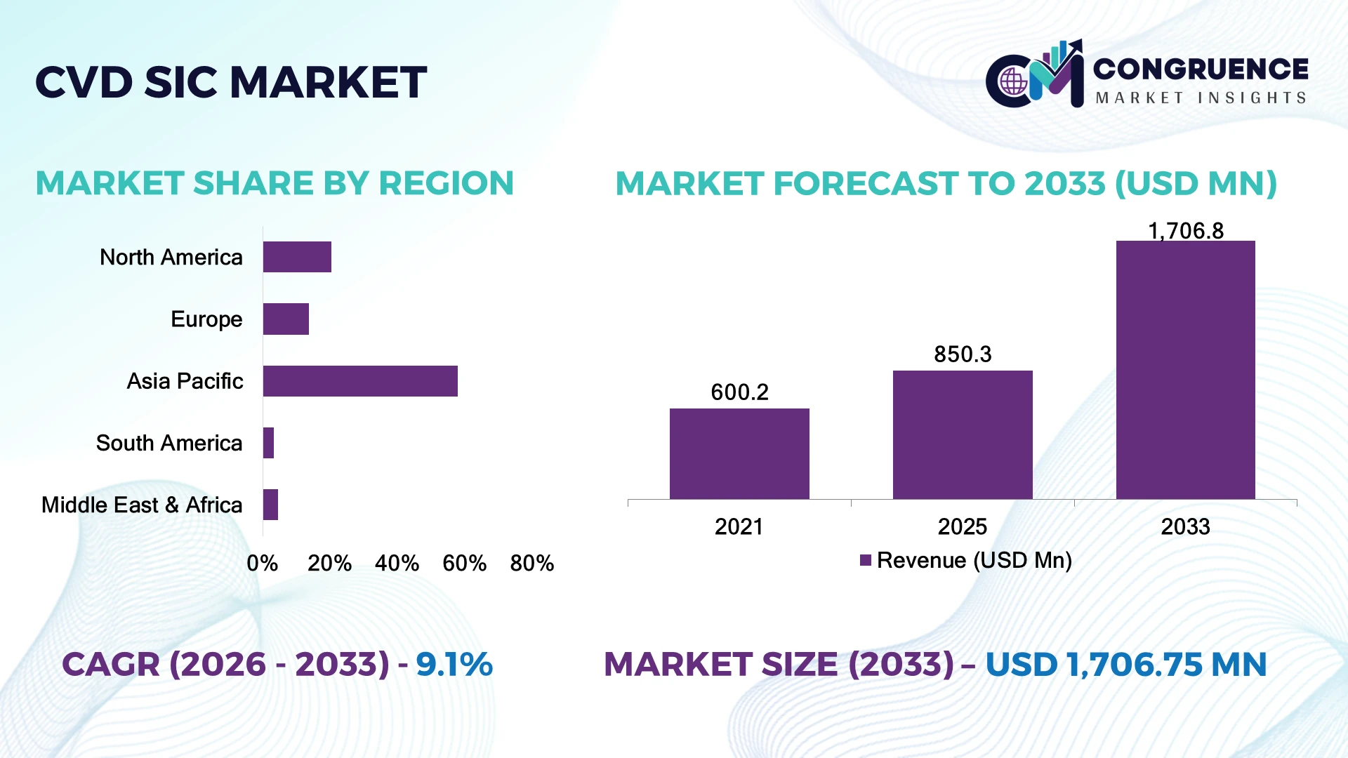
China is the dominant CVD SiC production and consumption hub, supported by expanding SiC wafer, power-device and conductor equipment capacity, with the country representing roughly 40% of Asia-Pacific demand. Japan retains a high-purity materials advantage, while the United States prioritizes power electronics and defense applications. India’s 60,000-wafer SiC fab plan signals supply-chain diversification beyond East Asia.
Suppliers combining ultra-high purity, coating uniformity, automated deposition, and regional manufacturing capacity are best positioned to capture conductor-led CVD SiC demand.
Market Size & Growth: USD 850.3 million in 2025 to USD 1,706.8 million by 2033 at 9.1%, driven by conductor-grade thermal components.
Top Growth Drivers: conductor equipment 34%, SiC power devices 29%, and high-temperature components 18% lead demand.
Short-Term Forecast: By 2028, automated controls can cut coating rework 8–12% and improve deposition consistency 3–5%.
Emerging Technologies: AI reactor control, CFD optimization, 3C-SiC films, and ultra-high-purity coatings are tightening defect control.
Regional Leaders: Asia-Pacific approaches USD 900 million by 2033, North America USD 400 million, and Europe USD 260 million.
Consumer/End-User Trends: conductor applications represent more than 60% of demand, led by coated susceptors and wafer-processing components.
Pilot/Case Example: A 2026 study achieved 42.12 GPa hardness while maintaining coating stability during 1,100°C GaN growth.
Competitive Landscape: Asia-Pacific leads at roughly 45%, with Tokai Carbon, CoorsTek, SGL Carbon, Toyo Tanso, and Ferrotec competing on purity and lead time.
Regulatory & ESG Impact: India’s approved SiC project targets 60,000 wafers annually, strengthening regional conductor supply resilience.
Investment & Funding: India’s SiCSem project carries INR 2,066 crore of approved investment, accelerating integrated SiC manufacturing.
Innovation & Future Outlook: Next-generation CVD SiC targets 99.9999% purity, lower defects, thicker coatings, and digitally controlled reactors.
CVD SiC demand is concentrated in conductor susceptors, wafer-processing parts, epitaxy hardware, and high-temperature protective coatings. Ultra-high-purity grades, tighter coating uniformity, and digitally controlled deposition are gaining traction, while 3C-SiC research expands application potential. conductor localization in India and East Asia is strengthening regional sourcing, with high-purity applications already exceeding 60% of demand. These shifts are reshaping qualification and sourcing decisions.
CVD SiC is becoming strategically important because conductor manufacturers increasingly treat coated graphite, thermal-field components, and high-purity reactor parts as yield-critical assets rather than commodity consumables. The market is shifting with conductor supply-chain localization as India, China, Japan, and the United States expand domestic SiC capabilities. This increases the value of suppliers that meet tighter purity, thickness, and repeatability requirements.
Modern CVD control using CFD, automated gas-flow management, and in-line metrology can reduce coating rework by roughly 8–12% versus less controlled batch practices while improving thickness consistency by 3–5%. Asia-Pacific remains the largest deployment base because of dense wafer and equipment ecosystems; North America emphasizes power electronics, aerospace, and defense, while Europe focuses on automotive electrification and specialized conductor equipment.
Over the next 2–3 years, suppliers should prioritize reactor automation, ultra-high-purity materials, and regional finishing capacity, with 99.9999% purity increasingly relevant for demanding conductor components. Deployment is expanding around coated graphite susceptors used in high-temperature epitaxy and MOCVD, where coating stability influences particle control and equipment life. Competitive advantage will favor validated recipes, faster qualification, localized inventory, and fab-equipment partnerships.
conductor fabrication is increasing demand for high-purity CVD SiC components as tighter particle and thermal-control requirements raise the cost of process contamination. conductor applications already represent more than 60% of CVD SiC demand, while ultra-high-purity grades above 99.999% increasingly support demanding epitaxy and wafer-processing environments. Japan and China are expanding SiC wafer capacity, reinforcing domestic sourcing requirements. India’s conductor localization program is adding further equipment demand. Companies are responding with automated deposition, tighter gas-flow control, and localized coating capacity. The non-obvious advantage is yield protection: extending component life by 10–15% can reduce chamber interventions and improve fab utilization more effectively than simply lowering component purchase prices.
CVD SiC production remains capital- and energy-intensive, with high-purity processing requiring controlled deposition environments, specialized precursors, and extended furnace cycles. Energy and process inputs can represent 20–30% of manufacturing cost, while coating rework can add 8–12% to effective production expense when thickness or surface-defect specifications are missed. China’s concentration of upstream SiC processing also exposes buyers to qualification and logistics disruptions when supply conditions tighten. Companies are countering these constraints through multi-year procurement agreements, dual-source qualification, localized finishing, and reactor utilization improvements. The strategic limitation is not raw-material availability alone; it is the ability to maintain identical coating specifications across qualified production sites without extending conductor customer validation cycles.
Digital reactor control creates an underexploited opportunity to improve CVD SiC economics without changing the underlying material platform. Automated gas-flow management, machine vision, and predictive process control can reduce coating rework by 8–12% and improve thickness consistency by approximately 3–5%. In the United States and Japan, suppliers are increasingly positioning advanced coatings for high-temperature epitaxy and compound-conductor equipment. India offers another opportunity as new conductor fabrication projects create localized demand for qualified consumables. Companies are investing in sensor-integrated reactors, digital process twins, and application-specific coating recipes. A key strategic opportunity is recurring refurbishment: extending the usable life of coated graphite components can create service revenue while lowering customers’ replacement frequency and chamber downtime.
Scaling CVD SiC production requires maintaining identical purity, density, surface morphology, and coating thickness across reactors, plants, and customer qualification batches. Production deviations of even 2–3% in critical coating parameters can trigger additional inspection or requalification, while complex multi-step processes can increase cycle times by 10–20%. Japan’s established precision-material ecosystem sets demanding benchmarks as Chinese and Indian suppliers expand capacity. Workforce shortages in advanced materials processing further increase dependence on automated metrology and recipe control. Companies must invest in standardized reactor architectures, statistical process control, digital traceability, and specialist training. The long-term competitive differentiator will be reproducibility at scale, because conductor customers value consistent process performance more than nominal coating capacity.
AI-Controlled Deposition Gains Traction: AI-assisted reactor monitoring is increasingly linking gas flow, temperature, and pressure data, with automated controls targeting 3–5% tighter coating consistency and 8–12% lower rework. Japanese and Chinese producers are integrating predictive analytics to stabilize multi-batch production.
Component Refurbishment Becomes Strategic: Recoating programs are expanding as conductor fabs seek longer component lifecycles. Extending coated graphite service life by 10–15% can reduce replacement frequency and maintenance interruptions, encouraging suppliers to build dedicated refurbishment and inspection capabilities near major fabrication hubs.
India Builds Local Supply Capability: India’s conductor localization push is shifting procurement toward domestically qualified materials and equipment. The approved 60,000-wafer SiC project strengthens the addressable ecosystem, while suppliers are developing local partnerships to reduce imported component dependence and shorten qualification-to-delivery cycles.
Ultra-Pure Coatings Tighten Specifications: conductor customers increasingly prioritize 99.999%+ purity, low particle generation, and controlled surface morphology. Advanced CVD SiC coatings are replacing less durable alternatives in demanding thermal processes, prompting manufacturers to upgrade precursor handling, metrology, and contamination-control infrastructure rather than simply adding deposition capacity.
CVD SiC-coated components represent the leading type, accounting for approximately 54% of the market, supported by susceptors, wafer carriers, focus rings, and thermal-processing components used in conductor manufacturing. Their dominance reflects established qualification pathways, repeat refurbishment demand, and compatibility with existing graphite-based equipment. Bulk CVD SiC is the fastest-growing type, representing roughly 23% of demand, as manufacturers pursue thicker, mechanically robust components for high-temperature epitaxy and advanced wafer-processing environments. Its adoption is being reinforced by the industry's transition toward larger SiC wafers and more demanding thermal cycles.
Coatings remain the mature volume segment at approximately 54%, while bulk and engineered CVD SiC formats together are gaining strategic importance. Advanced grades account for around 20% of demand, emphasizing ultra-high purity and controlled microstructure. Companies are increasing deposition automation, developing application-specific geometries, and expanding refurbishment capabilities rather than competing solely on material pricing.
Conductor wafer processing is the leading application, representing approximately 62% of global CVD SiC demand. Susceptors, wafer carriers, showerheads, and other thermal-zone components are concentrated in high-volume fabrication environments where particle control and temperature uniformity directly influence yield. SiC epitaxy and compound-conductor processing is the fastest-growing application, accounting for roughly 18% and gaining momentum as manufacturers scale 150 mm and 200 mm platforms. The transition to larger wafers is particularly important because larger process areas increase requirements for dimensional stability, coating uniformity, and thermal-field control.
Traditional wafer-processing applications remain the commercial base at approximately 62%, while power-device fabrication, GaN-related processing, and specialized high-temperature applications expand from smaller installed bases. Companies are responding through automated coating inspection, integrated refurbishment, and tighter deposition recipes. This shifts purchasing toward lifecycle performance, with component consistency increasingly becoming an operational requirement rather than a procurement specification.
Conductor manufacturers and wafer fabrication facilities represent the leading end-user group, accounting for approximately 68% of CVD SiC demand. Their purchasing intensity is driven by continuous reactor operation, component replacement cycles, strict contamination specifications, and qualification requirements. Power conductor manufacturers are the fastest-growing end-user group, representing roughly 18% of demand as SiC MOSFET and diode production expands beyond automotive applications into industrial drives, renewable-energy systems, and data-center power infrastructure.
Large integrated device manufacturers remain the mature purchasing base, while specialized compound-conductor producers and equipment manufacturers collectively account for approximately 14%. Emerging buyers increasingly require customized coating thickness, thermal resistance, surface morphology, and chamber compatibility rather than standardized components. Companies are responding with long-term qualification agreements, regional inventories, dedicated refurbishment centers, and joint engineering programs. The strategic shift is toward supplier integration: manufacturers that can combine deposition, machining, inspection, refurbishment, and application engineering gain stronger customer retention and reduce qualification friction.
Asia-Pacific accounted for the largest market share at 57.8% in 2025 moreover, Asia-Pacific is also expected to register the fastest growth, expanding at a CAGR of 10.2% between 2026 and 2033.
Onshoring SiC manufacturing is reshaping high-purity component procurement
North America represented approximately 20.4% of the global CVD SiC market in 2025, supported by semiconductor equipment, power electronics, aerospace, and defense applications. Demand is concentrated around U.S. fabrication and equipment clusters, where domestic sourcing is becoming more important under semiconductor supply-chain localization. Bosch is investing USD 2 billion to transform its Roseville, California facility into a SiC semiconductor manufacturing site, supported by up to USD 225 million under the CHIPS Program. CVD SiC suppliers are responding by expanding coating capacity, developing application-specific reactor components, and establishing qualification programs closer to fabs. The strategic shift is toward locally qualified, high-purity components rather than lowest-cost imports.
United States Market Outlook: The United States remains North America's principal demand center, supported by semiconductor reshoring and power-device manufacturing. Bosch's Roseville expansion is particularly important because commercial SiC production is targeted for 2026, while the company plans substantially broader U.S. investment through 2031. This strengthens demand for domestic CVD SiC-coated components, refurbishment, and high-temperature processing hardware.
Integrated SiC manufacturing is strengthening European supply resilience
Europe accounted for approximately 13.8% of global CVD SiC demand in 2025, with Germany, Italy, France, and Austria forming the strongest industrial cluster. Semiconductor localization is increasing demand for high-purity processing components as automotive and industrial power-device capacity expands. STMicroelectronics' Catania SiC campus targets 15,000 wafers per week at full build-out, integrating substrate, epitaxy, front-end, and back-end production. The European Chips Act is reinforcing this manufacturing transition, with approved first-of-a-kind projects expected to increase EU semiconductor capacity by approximately 30% by 2030. CVD SiC suppliers are therefore prioritizing localized qualification, automated inspection, and long-term equipment partnerships.
Germany Market Outlook: Germany is Europe's most strategically significant CVD SiC market because of its concentration of automotive, industrial electronics, power-semiconductor, and equipment manufacturing. Infineon's Dresden Smart Power Fab represents a EUR 5 billion investment and creates up to 1,000 direct jobs, strengthening demand for advanced power-semiconductor production infrastructure. Suppliers are positioning around contamination control, thermal-processing components, and locally supported maintenance.
High-volume wafer expansion is accelerating localized CVD SiC demand
Asia-Pacific accounted for approximately 57.8% of global CVD SiC demand in 2025, led by China, Japan, South Korea, and Taiwan. The region combines the largest concentration of semiconductor fabs with rapidly expanding 200 mm SiC production. China alone represents roughly 40% of regional CVD SiC demand, while new 8-inch SiC projects are increasing requirements for high-purity susceptors, wafer carriers, and epitaxy components. Several Asian manufacturers are transitioning from 150 mm to 200 mm platforms, improving wafer economics and increasing component requirements per production line. Suppliers are responding with localized coating plants, automated deposition, and direct qualification partnerships with wafer and equipment manufacturers.
China Market Outlook: China is the region's largest CVD SiC consumption and manufacturing center, supported by domestic power-device production and semiconductor-equipment localization. The country's 8-inch SiC expansion includes large-scale projects targeting hundreds of thousands of wafers annually, increasing demand for repeatable high-purity coatings and thermal-field components. Local suppliers are increasingly integrating deposition, machining, refurbishment, and inspection to shorten qualification cycles and reduce dependence on imported components.
Semiconductor localization is creating an early-stage industrial opportunity
South America accounted for approximately 3.4% of global CVD SiC demand in 2025, with Brazil representing the overwhelming majority of regional activity. Current consumption remains concentrated in semiconductor assembly, electronics manufacturing, research infrastructure, and emerging power-electronics applications rather than large-scale SiC wafer fabrication. Brazil's semiconductor ecosystem is nevertheless receiving stronger institutional support: the government aims to increase its share of the global semiconductor chain from 1% to 2% by 2033, while more than 85% of chips used domestically are imported. This import dependency creates an opening for qualified CVD SiC component suppliers as local capabilities mature. Companies are emphasizing technical partnerships, distributor networks, refurbishment services, and application engineering rather than building standalone deposition capacity prematurely.
Brazil Market Outlook: Brazil is the region's most commercially relevant market because of its established electronics base and expanding semiconductor policy framework. In June 2026, BNDES approved BRL 143.3 million for Zilia Technologies to expand and modernize semiconductor production in Atibaia, São Paulo. Such investment strengthens the downstream ecosystem and creates incremental demand for specialized thermal-processing and high-purity semiconductor components.
Industrial diversification is creating selective semiconductor demand
Middle East & Africa represented approximately 4.6% of global CVD SiC demand in 2025, with demand concentrated in Saudi Arabia, the United Arab Emirates, Israel, and selected African technology and research clusters. Semiconductor fabrication remains limited, but industrial diversification, advanced electronics, energy infrastructure, and technology investment are expanding the addressable market. Saudi Arabia is actively attracting international industrial capital through partnerships designed to strengthen manufacturing and supply-chain capabilities under Vision 2030. CVD SiC adoption therefore remains application-led, particularly in high-temperature industrial components and advanced power electronics. Suppliers are favoring partnerships, technical distribution, and localized service capability over capital-intensive manufacturing footprints.
Saudi Arabia Market Outlook: Saudi Arabia offers the strongest long-term opportunity in the region because its industrial strategy increasingly links advanced manufacturing with domestic supply-chain development. Institutional investment is being directed toward attracting international industrial expertise and sustainable manufacturing capabilities. For CVD SiC suppliers, the practical entry model is partnership-led: establish application engineering, inventory, and refurbishment capabilities first, then scale localized production as semiconductor and power-electronics infrastructure reaches commercial volume.
Tokai Carbon, Morgan Advanced Materials, Ferrotec, CoorsTek, and SGL Carbon compete as global technology leaders, while Chinese suppliers compete primarily on cost, localization, and delivery speed. The top five players collectively hold approximately 54% share. Competition centers on purity, coating uniformity, customization, and supply reliability, with advanced suppliers targeting 99.999%+ purity and 3–5% tighter process consistency. Players are expanding coating capacity, integrating machining and refurbishment, and forming semiconductor-fab partnerships. Tokai Carbon is strengthening Korean operations, while SGL Carbon is expanding U.S. and European capabilities. The competitive shift is moving from standalone coating supply toward integrated component engineering and localized qualification. Entry barriers remain high because semiconductor customers require lengthy process validation, contamination control, and repeatable coating specifications. Cost-focused Chinese manufacturers face pressure to demonstrate equivalent reliability rather than simply lower pricing. Winning requires proprietary deposition recipes, high-purity processing, rapid qualification, regional capacity, and integrated lifecycle support.
Tokai Carbon Co., Ltd.
Morgan Advanced Materials plc
Ferrotec Holdings Corporation
CoorsTek, Inc.
AGC Inc.
SKC solmics
SGL Carbon SE
Toyo Tanso Co., Ltd.
Mersen
KNJ Co., Ltd.
Zhicheng Semiconductor
Hunan Dezhi Material Technology
Zhejiang Liufang Semiconductor Technology
Momentive Technologies
CVD reactor automation is shifting from fixed recipes toward sensor-driven deposition control, combining temperature, pressure, gas-flow and optical monitoring. Closed-loop systems can improve coating uniformity by 1–2% and reduce process deviations by 2–3%. Adoption is strongest among high-volume semiconductor suppliers, where automated recipe control protects yield and shortens qualification cycles.
CFD-assisted reactor design and digital process twins are emerging as practical tools for large-area coating optimization. Recent process research demonstrates tighter control of stoichiometry and surface morphology through coupled thermodynamic-fluid-dynamic modeling. Compared with conventional empirical tuning, simulation-led optimization can reduce development iterations by 10–15%, benefiting suppliers serving larger susceptors and increasingly complex geometries.
Ultra-high-purity CVD SiC, advanced TaC interfaces, and integrated metrology represent the disruptive layer through 2026–2028. Coatings above 6N purity and hardness above 42 GPa demonstrate the performance ceiling for semiconductor-grade components. Automated inspection can improve defect-screening throughput by 20–30%, while integrated refurbishment extends component utilization. Technology leaders with proprietary recipes, high-purity processing, and customer-specific qualification data will gain the strongest advantage as fabs demand tighter contamination control, larger wafer compatibility, faster changeovers, and localized supply. These capabilities also reduce requalification exposure and strengthen long-term customer integration across critical process equipment while improving asset utilization and production continuity.
March 2026 SGL Carbon reported €43.2 million in 2025 Graphite Solutions capital expenditure, with SiC coating capacity expanded at St. Marys. The investment strengthens U.S. semiconductor supply resilience and supports localized component qualification for advanced semiconductor manufacturing customers. Source: sglcarbon.com
April 2024 Tokai Carbon acquired 350,000 additional shares of Tokai Carbon Korea for ¥5.199 billion, strengthening control of its CVD-SiC coated-products operation. The transaction improves supply coordination and processing capabilities for semiconductor customers across Korea’s advanced semiconductor ecosystem. Source: tokaicarbon.co.jp
November 2025 Linköping University and SGL Carbon opened a coating laboratory with one purpose-built CVD tool. The facility accelerates qualification of next-generation coatings for semiconductor components, strengthening European innovation and shortening the path from research to customer testing. Source: liu.se
December 2025 China Building Materials Academy research demonstrated CVD-SiC coatings exceeding 6N purity and 42.12 GPa hardness, remaining stable through 100 GaN growth cycles. The result establishes tighter performance benchmarks for semiconductor-grade susceptors and advanced epitaxy equipment systems. Source: nature.com
The CVD SiC Market Report covers low-, middle-, and high-resistivity grades, with applications spanning rapid thermal processing components, plasma etch components, susceptors and dummy wafers, LED wafer carriers and cover plates, and specialized applications. End-user coverage emphasizes semiconductor manufacturers, wafer fabs, equipment OEMs, power-device producers, and compound-semiconductor manufacturers, with semiconductor applications representing more than 60% of demand.
Geographic coverage includes North America, Europe, Asia-Pacific, South America, and Middle East & Africa, with detailed country-level assessment of China, Japan, South Korea, Taiwan, the United States, Germany, and emerging manufacturing hubs. Technology coverage includes CVD deposition, reactor automation, CFD optimization, ultra-high-purity coatings, TaC interfaces, digital metrology, and refurbishment. The analysis supports capacity planning, supplier qualification, localization, investment decisions, competitive positioning, and expansion strategy through 2026–2033.
| Report Attribute/Metric | Report Details |
|---|---|
|
Market Revenue in 2025 |
USD 850.3 Million |
|
Market Revenue in 2033 |
USD 1,706.8 Million |
|
CAGR (2026 - 2033) |
9.1% |
|
Base Year |
2025 |
|
Forecast Period |
2026 - 2033 |
|
Historic Period |
2021 - 2025 |
|
Segments Covered |
By Type
By Application
By End-User
|
|
Key Report Deliverable |
Revenue Forecast, Growth Trends, Market Dynamics, Segmental Overview, Regional and Country-wise Analysis, Competition Landscape |
|
Region Covered |
North America, Europe, Asia-Pacific, South America, Middle East, Africa |
|
Key Players Analyzed |
Tokai Carbon Co., Ltd., Morgan Advanced Materials plc, Ferrotec Holdings Corporation, CoorsTek, Inc., AGC Inc., SKC solmics, SGL Carbon SE, Toyo Tanso Co., Ltd., Mersen, KNJ Co., Ltd., Zhicheng Semiconductor, Hunan Dezhi Material Technology, Zhejiang Liufang Semiconductor Technology, Momentive Technologies |
|
Customization & Pricing |
Available on Request (10% Customization is Free) |